

Philips sa5753 DATASHEETS

INTEGRATED CIRCUITS
SA5753
Audio processor — filter and control
section
Product specification
Replaces data of 1995 July 7
IC17 Data Handbook
1997 Nov 07
Philips Semiconductors Product specification
SA5753Audio processor – filter and control section
DESCRIPTION
The SA5753 is a high performance low power CMOS audio signal
processing system especially designed to meet the requirements for
small size and low voltage operation of hand-held equipment. The
SA5753 subsystem includes complementary transmit/receive voice
band (300-3000Hz), switched capacitor bandpass filters with
pre-emphasis and de-emphasis respectively, a transmit low pass
filter, peak deviation limiter for transmit, digitally controlled
attenuators for signal level and volume control, audio path mute
switches, a programmable DTMF generator, power-down circuitry
for low current standby, power-on reset capability, and an I
2
C
interface. When the SA5753 is used with an SA5752 (companding
function), the complete audio processing system of an AMPS,
TACS, NAMPS or NTACS cellular telephone is easily implemented.
The system also meets the requirements of the proposed NAMPS or
NTACS specification, and can be used in cordless telephone
applications.
The SA5753 can be operated without the I
2
C bus interface by
pulling DFT (Pin 13) HIGH.
BENEFITS
•Very compact application
•Long battery life in portable equipment
•Complete cellular audio function with the SA5752
APPLICATIONS
•Cellular radio
•Mobile communications
•High performance cordless telephones
•2-way radio
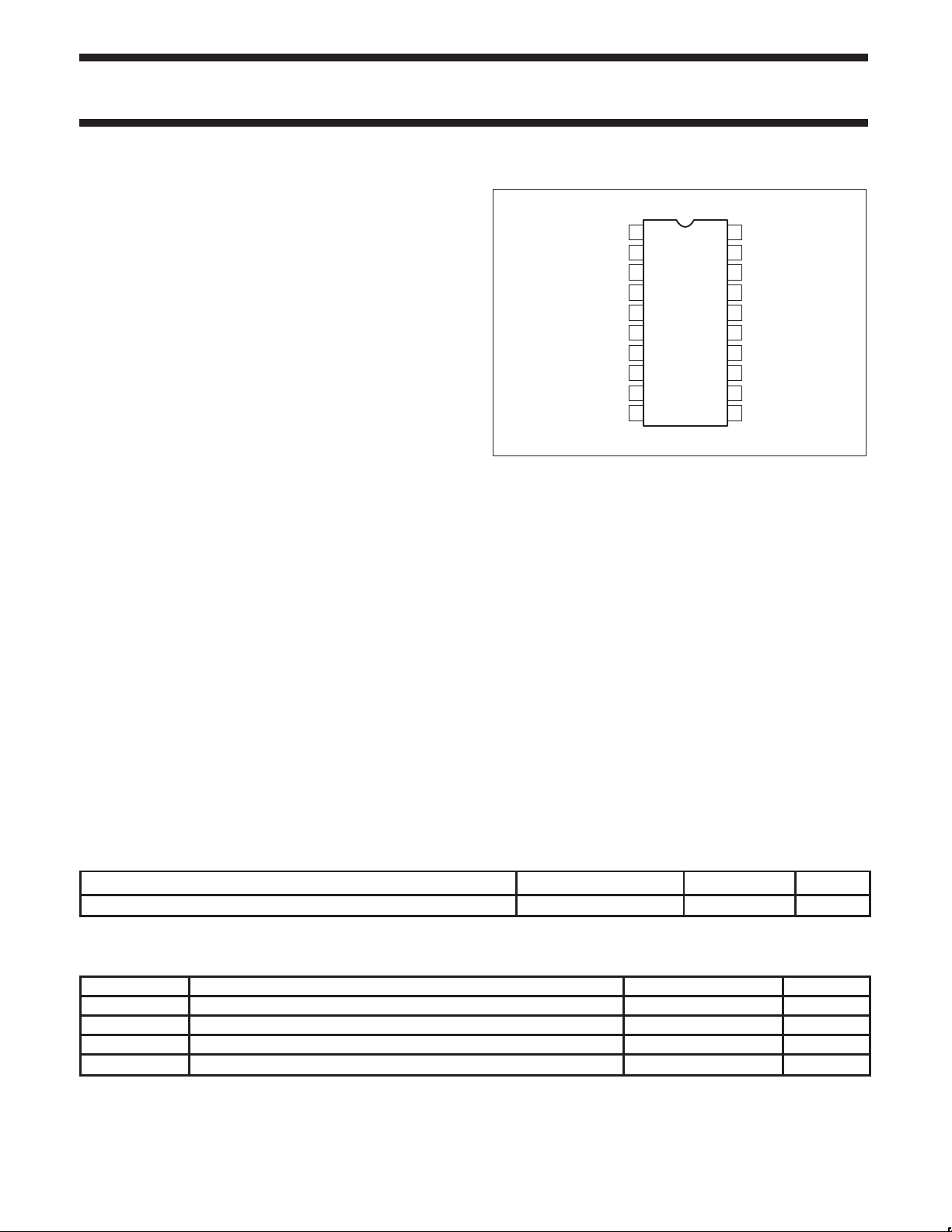
PIN CONFIGURATION
DK Package
TXBF
TXBF
PREMP
VOX
DEMP
AUDIO
SPKR
EAR
OUT
V
DD
CTL
HPDN
OUT
OUT
OUT
1
IN
2
3
IN
4
5
6
SA5753
7
8
IN
9
10
20
19
18
17
16
15
14
13
12
11
TX
OUT
DATA
IN
TX MUTE
SDA
SCL
GND
CLK
IN
DFT
RX MUTE
RX DEMOD
IN
SR00666
Figure 1. Pin Configuration
FEATURES
•Low 3V supply
•Miniature SSOP package
•Low power
•High performance
•Built-in programmable DTMF generator
•Built-in digitally controlled attenuators for modulation and volume
control
•Built-in peak-deviation limiter
2
•I
C Bus controlled
•Power-on reset
•Power down capability
•Programmable mute control
•Meets AMPS/TACS/NAMPS/NTACS requirements
ORDERING INFORMATION
DESCRIPTION TEMPERATURE RANGE ORDER CODE DWG #
20-Pin Plastic Shrink Small Outline Package (SSOP) -40 to +85°C SA5753DK SOT266-1
ABSOLUTE MAXIMUM RATINGS
SYMBOL PARAMETER RATING UNIT
V
DD
V
IN
T
A
1997 Nov 07 853-1722 18666
Power supply voltage range -0.3 to 6 V
Voltage applied to any other pin -0.3 to VDD+0.3 V
Storage temperature -65 to +150
Ambient operating temperature -40 to +85
2
o
°C
C
Philips Semiconductors Product specification
SA5753Audio processor – filter and control section
PIN DESCRIPTIONS
PIN NO. SYMBOL DESCRIPTION
1 TXBF
2 TXBF
3 PREMP
4 V
5 VOX
IN
OUT
IN
DD
CTL
6 HPDN Power-down I/O
7 DEMP
8 AUDIO
9 SPKR
10 EAR
11 RX DEMOD
OUT
IN
OUT
OUT
IN
12 RX MUTE RX audio signal mute input
13 DFT Default input, non-I2C or stand-alone operation
14 CLK
IN
15 GND Ground
16 SCL I2C serial clock line
17 SDA I2C serial data line
18 TX MUTE Tx audio signal mute input
19 DATA
20 TX
IN
OUT
Transmit bandpass filter input
Transmit bandpass filter output
Pre-emphasis input
Positive supply
Vox control output
De-emphasis output
Audio input
Audio output to speaker
Audio output to earpiece
Rx demodulated audio signal input
Clock input (1.2MHz)
Data input
Transmit output
1997 Nov 07
3
Philips Semiconductors Product specification
SYMBOL
PARAMETER
TEST CONDITIONS
UNIT
SYMBOL
PARAMETER
TEST CONDITIONS
UNIT
SA5753Audio processor – filter and control section
DC ELECTRICAL CHARACTERISTICS
TA = 25oC, VDD = +3.3V , unless otherwise specified. See test circuit, Figure 2.
LIMITS
MIN TYP MAX
V
DD
I
DD
I
IH
I
IL
V
V
AC ELECTRICAL CHARACTERISTICS
TA = 25oC, VDD = +3.3V. See test circuit, Figure 2. Clock frequency = 1.2MHz; test level = 0dBV = 77.5mV
specified. All gain control blocks (Attenuators) = 0dB gain, NAMPS and VCO bits set to 0.
Power supply voltage 3.0 3.3 5.5 V
Operating
Supply current
IDLE
Power Down (PWDN)
Input current high
TX MUTE, RX MUTE, HPDN
DFT
Input current low
TX MUTE, RX MUTE,
HPDN, DFT
Input voltage high 0.7V
IH
Input voltage low 0 0.3V
IL
VIN = V
DD
VIN = GND
–10
0
–30
–10
DD
1.7
600
200
0
+10
+10
+30
–10
0
+10
V
= -20dBm, unless otherwise
RMS
LIMITS
MIN TYP MAX
RX BPF anti alias rejection 40 dB
RX BPF input impedance f= 1kHz 100 kΩ
RX BPF gain with de-emphasis f = 1kHz -1.0 0 1.0 dB
RX BPF gain with de-emphasis f = 100Hz -30 dBm0
RX BPF gain with de-emphasis f = 300Hz 8.5 9.6 11.5 dBm0
RX BPF gain with de-emphasis f = 3kHz -11.5 -10.0 -8.5 dBm0
RX BPF gain with de-emphasis f = 5.9kHz -58 dBm0
RX BPF noise with de-emphasis 300Hz-3kHz 200 µV
RX dynamic range with deemphasis 80 dB
DEMP
DEMP
SPKR
EAR
SPKR
output impedance f = 1kHz 40 Ω
OUT
output swing (1%) 2kΩ to V
OUT
ouput swing (1%) 50kΩ toV
OUT
output swing (1%) 50kΩ to V
OUT
noise / EAR
OUT
noise 200 µV
OUT
; f = 1kHz 2.4 V
DD/2
; f = 1kHz VDD -1 2.4 V
DD/2
f = 1kHz VDD -1 2.4 V
DD/2;
CLKIN high 2.1 3.0 V
CLKIN low 0 1.0 V
TX BPF anti alias rejection f > 50kHz 40 dB
TX BPF input impedance f = 3kHz 100 KΩ
TX BPF noise 300 - 3000kHz 200 µV
TX LPF gain f = 5.9kHz -39 -36 dBm0
TX LPF gain with pre-emphasis f = 1kHz, 0dBV 2.43 dB
TX LPF gain with pre-emphasis f = 100Hz -19 dBm0
TX LPF gain with pre-emphasis f = 300Hz -10.45 dBm0
TX LPF gain with pre-emphasis f = 3kHz 9.14 dBm0
TX LPF gain with pre-emphasis f = 5900Hz -28 dBm0
TX LPF gain with pre-emphasis f = 9kHz -48 dBm0
TX overall gain 1kHz 2.43 dB
TX overall gain 100Hz -58 -44 dBm0
TX overall gain 300Hz -11.5 -10.4 -8.5 dBm0
0
DD
DD
mA
µA
µA
µA
µA
µA
µA
V
V
RMS
P-P
P-P
P-P
RMS
RMS
1997 Nov 07
4
Philips Semiconductors Product specification
SYMBOL
PARAMETER
TEST CONDITIONS
UNIT
SYMBOL
Bits
TYPICAL STEP (dB)
SA5753Audio processor – filter and control section
AC ELECTRICAL CHARACTERISTICS (continued)
LIMITS
MIN TYP MAX
TX overall gain 3kHz 8 9 9.6 dBm0
TX overall gain 5.9kHz -52 -45 dBm0
TX BPF dynamic range TBD dB
PREMP
TX
Tx DTMF signal with TXLPF and pre-emphasis 0.45 V/kHz
Rx DTMF sidetone –0.8 5.2 dBm0
input impedance f = 3kHz 100 kΩ
IN
Slew rate CL = 15pF 0.75 V/µs
OUT
Output impedance f = 3kHz 40 Ω
Output swing (limiting) 1.2 V
Output swing (1% THD)
5kΩ load (25°C)
1.0 V
P-P
P-P
Time delay to mute from RX MUTE or TX MUTE
transition
VIN = VIL to V
VIN = VIH to V
Table 1. Gain Control Blocks (Bit 0 is Least Significant Bit)
A1 4 –0.8 –12.0 0
A2a 5 ±0.25 –3.75 +3.75
A2b 2 –6, (–12 on first) –24.0 0
A3 4 –1.0 –17.0 –2.0
A4 4 ±0.5 –3.5 +3.5
A6 4 –2.0 –30.0 0
A7 4 ±0.5 –3.5 +3.5
NAMPS 1
VCO 1 +6.0 in A4
MSB sets the sign of the gain
For A2a, A4 and A7:
MSB = 0 for gain
MSB = 1 for attenuation
For all Gain Blocks:
FUNCTIONAL DESCRIPTION
All bits set to 0 = 0dB gain
All bits set to 1 = maximum gain or attenuation
a. A1 compensates for microphone gain variations in the transmit
The SA5753 is an audio signal processor designed to meet the
requirements of compact low voltage radio telephone equipment. It
includes transmit and receive bandpass filters for voiceband
b. A2a compensates for transmitter dynamic range variations due to
(300-3000Hz) with pre-emphasis and de-emphasis respectively, a
transmit peak deviation limiter , voice channel mute switches and a
data path which can be summed into the transmit channel. An I
2
C
interface is provided for software programmability of a DTMF
generator, mute polarity, selection of different power down and
operating modes and control of the gain in both the transmit and
c. A2b allows coarse attenuation to be inserted in the transmit path
receive channels.
Software programmable gain control allows the device to be
automatically optimized during equipment production and offers
d. A3 sets the gain between the DA TA
flexibility during normal operation.
Gain Blocks
The programmable gain blocks are shown in Table 1 and Figure 2.
The purpose for each block is as follows:
IH
IL
0.5
0.5
µs
µs
TYPICAL GAIN (dB)
MIN MAX
+1.9 in A2b
–7.6 in A4
path.
manufacturing tolerances of the SA5753 and SA5752 compandor
companion device. To meet AMPS requirements, the dynamic
range between the zero crossing signal level of the compandor
and the peak signal allowed by the deviation limiter is adjusted to
12.34dB.
to eliminate positive feedback effects in hands-free speaker
applications. First step is 12dB followed by two steps of 6dB.
pin (Pin 19) and the TX
IN
OUT
pin (Pin 20) and should be adjusted after A2a and A4 have been
previously optimized. The SA5753 will interface directly with the
UMA1000T data processor (which produces a 2Vpk data signal).
For NAMPS applications an additional 10 to 14dB resistive divider
must be added at the DATA
pin (Pin 19) for a 2V data signal.
IN
1997 Nov 07
5
 Loading...