Philips sa5752 DATASHEETS

RF COMMUNICATIONS PRODUCTS
SA5752
Audio processor – companding, VOX and
amplifier section
Product Specification
Replaces data of December 6, 1993
IC17 Data Handbook
Philips Semiconductors
1997 Nov 07

Philips Semiconductors Product specification
SA5752Audio processor – companding, VOX and amplifier section
DESCRIPTION
The SA5752 is a high performance low power audio signal
processing system especially designed to meet the requirements for
small size and low voltage operation of hand-held equipment. The
SA5752 subsystem includes a low noise microphone preamplifier
with adustable gain, a noise cancellation switching amplifier with
adjustable threshold, a voice operated transmitter (VOX) switch,
VOX control, an audio compressor with buffered input, audio
expandor, and an internal bandgap voltage regulator with power
down capability . When used with Philips Semiconductors’ SA5753,
the complete audio processing function of an AMPS or TACS
cellular telephone is easily implemented. The system also meets
the requirements of the proposed NAMPS or NTACS specifications.
The SA5752 can also be used without the SA5753 in a wide variety
of radio communications applications.
FEA TURES
• Operating voltage range: 2V to 5.5V
• Miniature SSOP
• High performance
• Adjustable VOX and noise cancellation threshold
• Adjustable gain preamplifier
• Audio companding
• ESD protected
• Open collector VOX output
• Logic inputs CMOS compatible
• Power down mode
• Few external components
• Meets AMPS/TACS/NAMPS/NTACS requirements
PIN CONFIGURATION
DK PACKAGE
PREAMP
RECT
NCAN
VOX
EXP
MIC
GRES
VOX
V
IN
GRES
CAP
OUT
TR
GND
REF
V
CC
CAP
1
2
3
4
5
6
SA5752
7
8
9
10
20
NCAN
19
COMP
18
COMP
COMP
17
16
COMP
15
COMP
14
VOX
CTL
13
HPDN
12
EXP
IN
EXP
11
OUT
Figure 1. Pin Configuration
BENEFITS
• Very compact applications
• Long battery life in portable equipment
• Complete cellular audio function with the SA5753
APPLICATIONS
• Cellular radio
• Mobile communications
• High performance cordless telephones
• 2-way radio
OUT
IN
CAP3
CAP1
OUT
CAP2
SR00659
ORDERING INFORMATION
DESCRIPTION TEMPERATURE RANGE ORDER CODE DWG #
20-Pin Plastic Shrink Small Outline Package (SSOP) -40 to +85°C SA5752DK SOT266-1
1997 Nov 07 853-1721 18666
2

Philips Semiconductors Product specification
SA5752Audio processor – companding, VOX and amplifier section
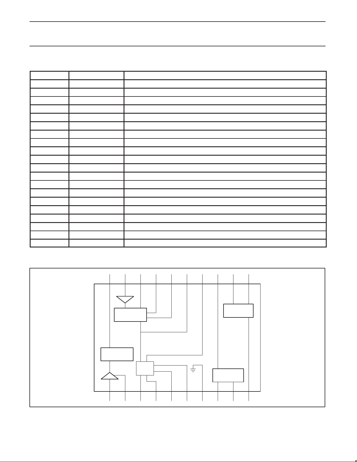
PIN DESCRIPTIONS
PIN NO. SYMBOL DESCRIPTION
1 MIC
2 PREAMP
3 RECT
4 NCAN
5 VOX
6 VOX
IN
GRES
GRES
CAP
OUT
TR
7 GND Ground
8 V
9 V
10 EXP
11 EXP
12 EXP
REF
CC
CAP
OUT
IN
13 HPDN Hardware power-down
14 VOX
15 COMP
16 COMP
17 COMP
18 COMP
19 COMP
20 NCAN
CTL
CAP2
OUT
CAP1
CAP3
IN
OUT
Microphone input
Preamplifier gain resistor
Rectifier gain resistor
Noise cancellation timing capacitor
Voice operated transmission output
Voice operated transmission threshold resistor
Reference voltage
Positive supply
Expandor timing capacitor
Expandor output
Expandor input
Voice operated transmission control
Compressor capacitor 2 DC block
Compressor output
Compressor timing capacitor 1
Compressor capacitor 3 DC block
Compressor input
Noise cancellation output
BLOCK DIAGRAM
COMPANDOR
NOISE
CANCEL
PREAMP
12 1120 19 18 17 16 15 14 13
BUFFER
EXPANDOR
SA5752
VOX
BANDGAP
VOLTAGE REF
10987654321
SR00660
Figure 2. Block Diagram
1997 Nov 07
3

Philips Semiconductors Product specification
SYMBOL
PARAMETER
TEST CONDITIONS
UNIT
SYMBOL
PARAMETER
TEST CONDITIONS
UNIT
SA5752Audio processor – companding, VOX and amplifier section
ABSOLUTE MAXIMUM RATINGS
SYMBOL PARAMETER RATING UNIT
V
CC
V
IN
T
STG
T
A
DC ELECTRICAL CHARACTERISTICS
TA = 25oC, VCC = +3.0V , 0dB = 77.5mV
V
CC
I
CC
Z
L
Z
IN
V
OS
NOTES:
1. Compressor is tested in production with 50kΩ load.
2. Not tested in production.
3. Offset values are identical for both gain states of noise reduction circuit.
4. Operational down to V
Power supply voltage range -0.3 to 6 V
Voltage applied to any other pin -0.3 to (VCC+0.3) V
Storage temperature -65 to +150
Ambient operating temperature -40 to +85
. See test circuit, Figure 6.
RMS
LIMITS
MIN TYP MAX
Supply voltage 2.7
Supply current
No signal
Power down mode
4
3.0 5.5 V
3.1
4.0 mA
125
µA
Load impedance
pins NCAN
COMP
OUT
OUT
1
, EXP
OUT
50 kΩ
10 kΩ
Input impedance
COMP
EXP
IN
IN
2
, MIC
IN
40 50 60 kΩ
2.0 kΩ
Noise cancellation current Pin 6 25 µA
= 2V.
OUT
3
-50 –3.0 50 mV
DC offset NCAN
CC
o
°C
C
AC ELECTRICAL CHARACTERISTICS
TA = 25oC, VCC = +3.0V , 0dB level = 77.5mV
Preamplifier gain range
Preamplifier voltage gain 0dB
Preamplifier voltage gain 40dB
Preamplifier noise density
Switch amplifier gain 9 10 11 dB
Compandor 1kHz, all tests
COMP
COMP
COMP
COMP
COMP
EXP
EXP
EXP
OUT
OUT
OUT
Compressor error at -21dB output level Input level = -42dB –1.0 –0.16 1.0 dB
OUT
Compressor error at -10dB output level Input level = -20dB -1.0 –0.11 1.0 dB
OUT
Compressor error at 0dB output level Input level = 0dB -1.5 +0.1 1.5 dB
OUT
Compressor error at +5dB output level Input level = +10dB -1.0 +0.04 1.0 dB
OUT
Compressor error at +10dB output level Input level = +20dB -1.0 +0.02 1.0 dB
OUT
Expandor error at -42dB output level Input level = -21dB –1.0 –0.12 1.0 dB
Expandor error at -21dB output level Input level = -10.5dB -1.0 +0.1 1.0 dB
Expandor error at -10dB output level Input level = -5dB -1.0 +0.03 1.0 dB
1
RMS
. See test circuit, Figure 6.
Pin 2 open
Pin 2 AC ground
Pin 2 AC grounded
RS = 50kΩ
unweighted 20Hz-20kHz
weighted CCIR
DIN45405 20-20kHz
LIMITS
MIN TYP MAX
0
-1.0
39.0
0
40
40
1.0
41.0
7
8
dB
dB
dB
nV/√Hz
nV/√Hz
1997 Nov 07
4
 Loading...