

Philips sa572 DATASHEETS

INTEGRATED CIRCUITS
SA572
Programmable analog compandor
Product specification 1998 Nov 03
IC17 Data Handbook
Philips Semiconductors Product specification
T
A
SA572Programmable analog compandor
DESCRIPTION
The SA572 is a dual-channel, high-performance gain control circuit
in which either channel may be used for dynamic range
compression or expansion. Each channel has a full-wave rectifier to
detect the average value of input signal, a linearized,
temperature-compensated variable gain cell (∆G) and a dynamic
time constant buffer. The buf fer permits independent control of
dynamic attack and recovery time with minimum external
components and improved low frequency gain control ripple
distortion over previous compandors.
The SA572 is intended for noise reduction in high-performance
audio systems. It can also be used in a wide range of
communication systems and video recording applications.
FEA TURES
•Independent control of attack and recovery time
•Improved low frequency gain control ripple
•Complementary gain compression and expansion with
external op amp
•Wide dynamic range—greater than 110dB
•T emperature-compensated gain control
•Low distortion gain cell
•Low noise—6µV typical
•Wide supply voltage range—6V-22V
•System level adjustable with external components
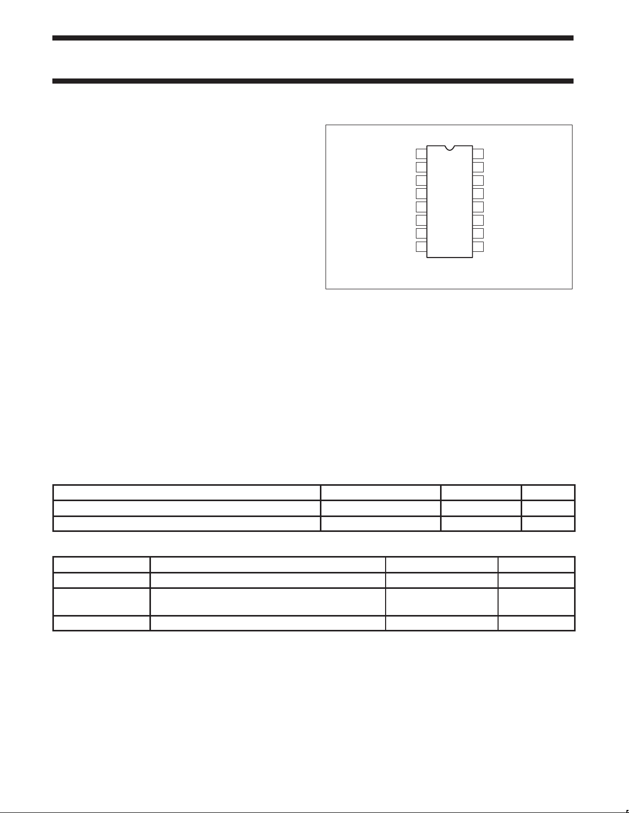
PIN CONFIGURATION
D1, N, Packages
TRACK TRIM A
RECOV. CAP A
RECT. IN A
ATTACK CAP A
∆G OUT A
THD TRIM A
NOTE:
1. D package released in large SO (SOL) package only.
1
2
3
4
5
6
∆G IN A
7
8
GND
Figure 1. Pin Configuration
APPLICATIONS
•Dynamic noise reduction system
•Voltage control amplifier
•Stereo expandor
•Automatic level control
•High-level limiter
•Low-level noise gate
•State variable filter
16
V
CC
15
TRACK TRIM B
14
RECOV. CAP B
13
RECT. IN B
12
ATTACK CAP B
∆G OUT B
11
10
THD TRIM B
∆G IN B
9
SR00694
ORDERING INFORMATION
DESCRIPTION TEMPERATURE RANGE ORDER CODE DWG #
16-Pin Plastic Small Outline (SOL) –40 to +85°C SA572D SOT162-1
16-Pin Plastic Dual In-Line Package (DIP) –40 to +85°C SA572N SOT38-4
ABSOLUTE MAXIMUM RATINGS
SYMBOL PARAMETER RATING UNIT
V
CC
P
D
Supply voltage 22 V
Operating temperature range
SA572 –40 to +85 °C
Power dissipation 500 mW
DC
1998 Nov 03 853-0813 20294
2
Philips Semiconductors Product specification
SYMBOL
PARAMETER
TEST CONDITIONS
UNIT
SA572Programmable analog compandor
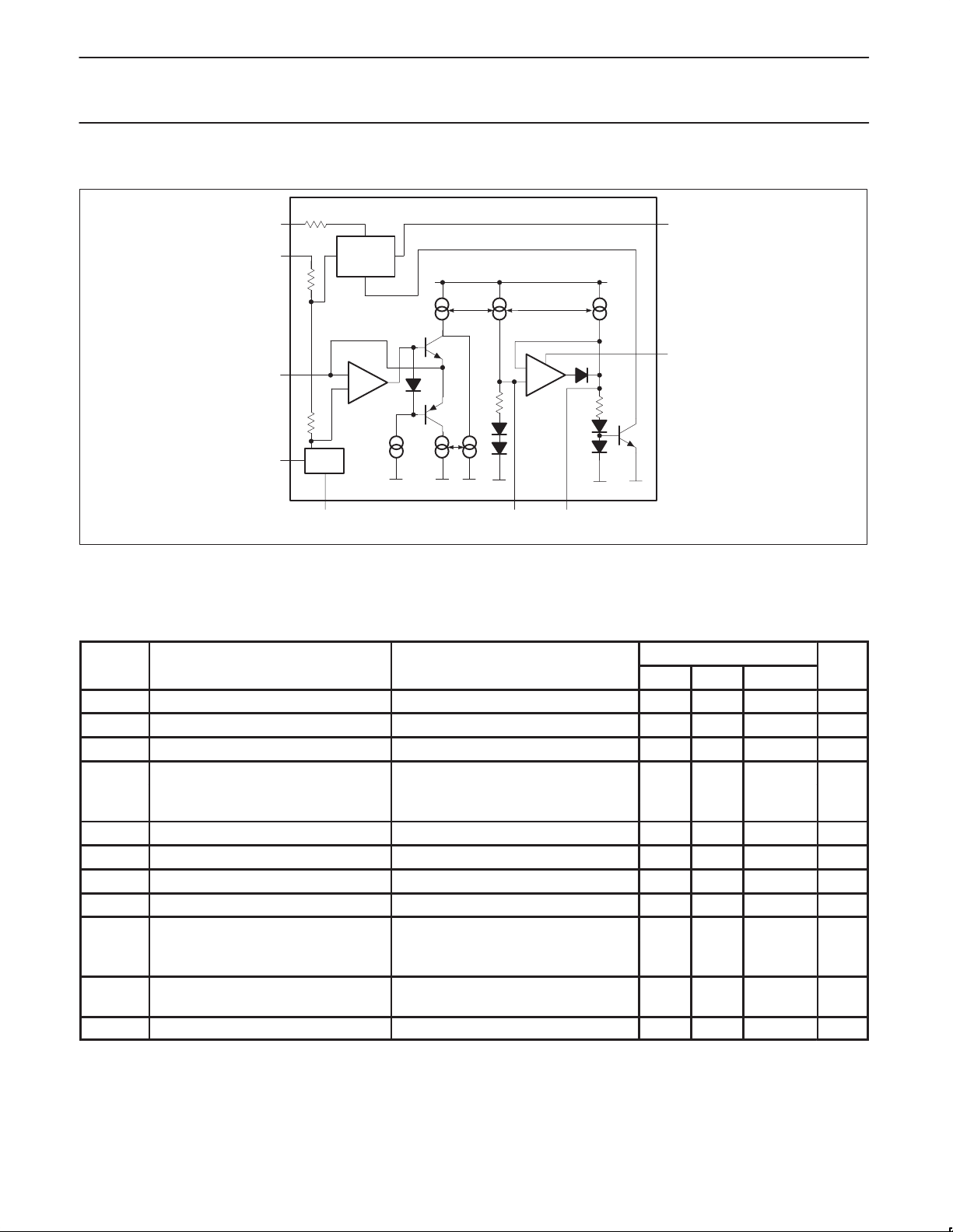
BLOCK DIAGRAM
(7,9)
(6,10)
(3,13)
(16)
R1
6.8k
∆G
500
Ω
GAIN CELL
–
+
270
Ω
RECTIFIER
P.S.
(8) (4,12) (2,14)
10k
–
+
BUFFER 10k
(5,11)
(1,15)
SR00695
Figure 2. Block Diagram
DC ELECTRICAL CHARACTERISTICS
Standard test conditions (unless otherwise noted) VCC=15V, TA=25°C; Expandor mode (see Test Circuit).
Input signals at unity gain level (0dB) = 100mV
V
CC
I
CC
V
R
Supply voltage 6 22 V
Supply current No signal 6.3 mA
Internal voltage reference 2.3 2.5 2.7 V
at 1kHz; V
RMS
1
THD Total harmonic distortion (untrimmed) 1kHz CA=1.0µF 0.2 1.0 %
THD Total harmonic distortion (trimmed) 1kHz CR=10µF 0.05 %
THD Total harmonic distortion (trimmed) 100Hz 0.25 %
No signal output noise Input to V1 and V2 grounded (20–20kHz) 6 25 µV
DC level shift (untrimmed) Input change from no signal to 100mV
Unity gain level –1.5 0 +1.5 dB
Large-signal distortion V1=V2=400mV 0.7 3 %
Tracking error
(measured relative to value at unity
gain)= [VO–VO (unity gain)]dB –V2dB
Channel crosstalk
PSRR Power supply rejection ratio 120Hz 70 dB
= V2; R
= 3.3kΩ; R
2
= 17.3kΩ.
3
SA572
Min Typ Max
RMS
±20 ±50 mV
Rectifier input
V2=+6dB V1=0dB ±0.2 dB
V2=–30dB V1=0dB ±0.5 –2.5, +1.6 dB
200mV
measured output on channel B
into channel A,
RMS
60 dB
DC
DC
1998 Nov 03
3

Philips Semiconductors Product specification
SA572Programmable analog compandor
TEST CIRCUIT
2.2µF
V
1
5Ω
= 10µF
2.2µF
1%
R
2
3.3k (3,13)
V
2
(7,9)
6.8k
(2,14)
(4,12)
∆G
BUFFER
RECTIFIER
(5,11)
(6,10)
(8)
(1,15)
(16)
Figure 3. Test Circuit
AUDIO SIGNAL PROCESSING IC COMBINES VCA AND FAST ATTACK/SLOW RECOVERY LEVEL SENSOR
In high-performance audio gain control applications, it is desirable to
independently control the attack and recovery time of the gain
control signal. This is true, for example, in compandor applications
for noise reduction. In high end systems the input signal is usually
split into two or more frequency bands to optimize the dynamic
behavior for each band. This reduces low frequency distortion due
to control signal ripple, phase distortion, high frequency channel
overload and noise modulation. Because of the expense in
hardware, multiple band signal processing up to now was limited to
professional audio applications.
With the introduction of the Signetics SA572 this high-performance
noise reduction concept becomes feasible for consumer hi fi
applications. The SA572 is a dual channel gain control IC. Each
channel has a linearized, temperature-compensated gain cell and an
improved level sensor. In conjunction with an external low noise op
+
22µF
22µF
100Ω
V
+15V
–15V
0
SR00696
82k
1k +
2.2k
2.2µF
1%
R
17.3k
270pF
1µF
3
–
NE5234
+
.1µF
+
amp for current-to-voltage conversion, the VCA features low
distortion, low noise and wide dynamic range.
The novel level sensor which provides gain control current for the
VCA gives lower gain control ripple and independent control of fast
attack, slow recovery dynamic response. An attack capacitor C
with an internal 10k resistor RA defines the attack time tA. The
recovery time t
and an internal 10k resistor RR. Typical attack time of 4ms for
C
R
of a tone burst is defined by a recovery capacitor
R
the high-frequency spectrum and 40ms for the low frequency band
can be obtained with 0.1µF and 1.0µF attack capacitors,
respectively. Recovery time of 200ms can be obtained with a 4.7µF
recovery capacitor for a 100Hz signal, the third harmonic distortion
is improved by more than 10dB over the simple RC ripple filter with
a single 1.0µF attack and recovery capacitor, while the attack time
remains the same.
The SA572 is assembled in a standard 16-pin dual in-line plastic
package and in oversized SOL package. It operates over a wide
supply range from 6V to 22V . Supply current is less than 6mA. The
SA572 is designed for applications from –40°C to +85°C.
A
1998 Nov 03
4
 Loading...