

Philips SA56606-20GW, SA56606-27GW, SA56606-28GW, SA56606-29GW, SA56606-30GW Datasheet
...
INTEGRATED CIRCUITS
SA56606-XX
CMOS system reset
Product data
Supersedes data of 2001 Apr 24
File under Integrated Circuits, Standard Analog
2001 Jun 19
Philips Semiconductors Product data
SA56606-XXCMOS system reset
GENERAL DESCRIPTION
The SA56606-XX is a CMOS device designed to generate a reset
signal for a variety of microprocessor and logic systems. Accurate
reset signals are generated during momentary power interruptions
or whenever power supply voltages sag to intolerable levels. An
Open Drain output topology is incorporated for adaptability to a wide
variety of logic and microprocessor applications. Several reset
threshold versions of the device are available.
The SA56606-XX is available in the SOT23-5 surface mount
package.
FEA TURES
•12 V
maximum operating voltage
DC
•CMOS N-channel Open Drain output
•Offered in reset thresholds of
2.0, 2.7, 2.8, 2.9, 3.0, 3.1, 4.2, 4.3, 4.4, 4.5, 4.6, 4.7 V
•Available in SOT23-5 surface mount package
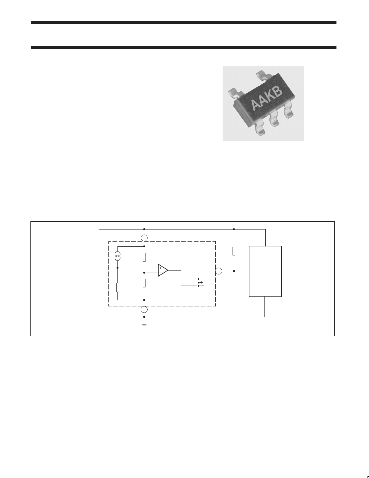
SIMPLIFIED SYSTEM DIAGRAM
V
DD
V
REF
R
V
SS
DC
V
2
R
R
3
V
DD
SA56606-XX
SS
APPLICATIONS
•Microcomputer systems
•Logic systems
•Battery monitoring systems
•Back-up power supply circuits
•Voltage detection circuits
R
PU
V
OUT
1
RESET
CPU
V
DD
V
SS
SL01313
Figure 1. Simplified system diagram.
2001 Jun 19 885–2247 26559
2
Philips Semiconductors Product data
TYPE NUMBER
SA56606-XXCMOS system reset
ORDERING INFORMATION
PACKAGE
NAME DESCRIPTION
SA56606-XXGW SOT23-5, SOT25, SO5 plastic small outline package; 5 leads (see dimensional drawing) –40 to +85 °C
TEMPERATURE
RANGE
NOTE:
The device has twelve detection voltage options, indicated by the
XX on the order code.
XX
DETECT VOLTAGE (Typical)
20 2.0 V
27 2.7 V
28 2.8 V
29 2.9 V
30 3.0 V
31 3.1 V
42 4.2 V
43 4.3 V
44 4.4 V
45 4.5 V
46 4.6 V
47 4.7 V
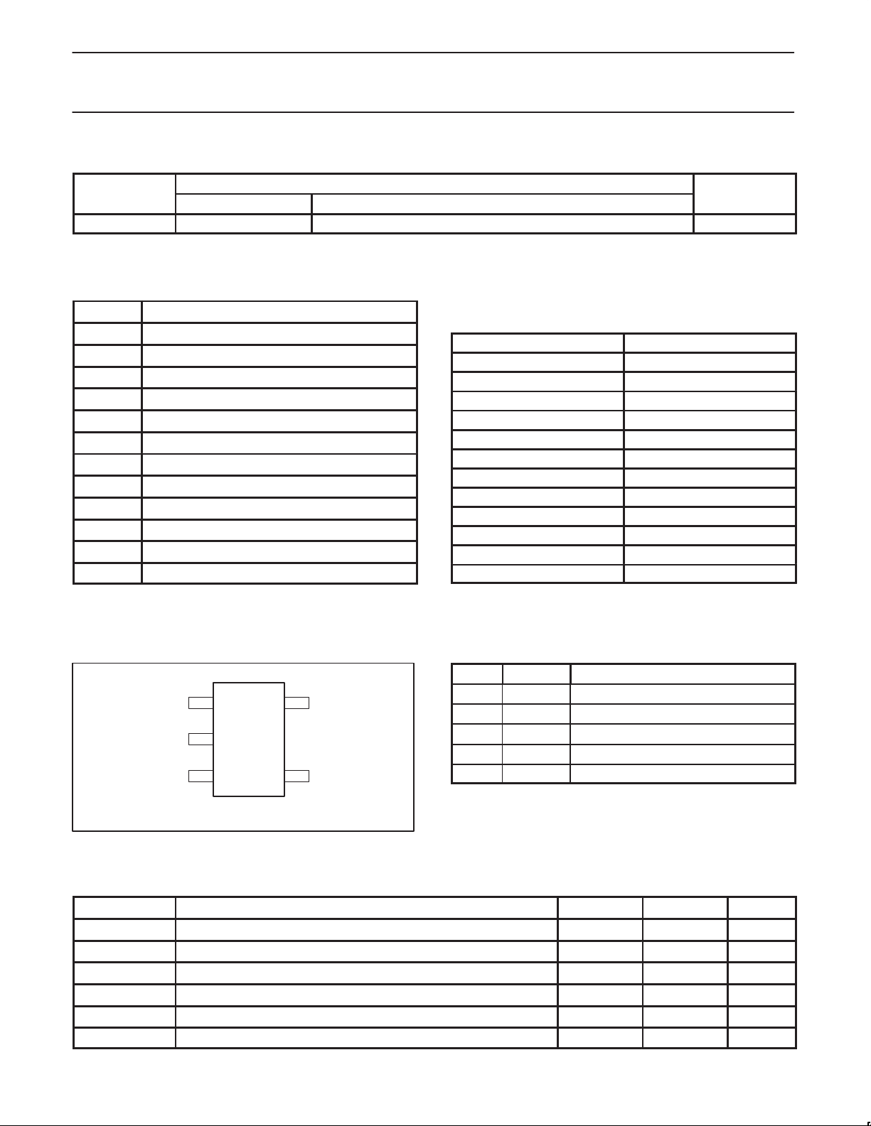
PIN CONFIGURATION
1
V
OUT
2
V
DD
SS
SA56606-XX
34
5 N/C
N/CV
Part number marking
Each package is marked with a four letter code. The first three
letters designate the product. The fourth letter, represented by ‘x’, is
a date tracking code. For example, AAKB is device AAK (the
SA56606-30 reset), produced in time period ‘B’.
Part number
Marking
SA56606-20 A A F x
SA56606-27 A A G x
SA56606-28 A A H x
SA56606-29 A A J x
SA56606-30 A A K x
SA56606-31 A A L x
SA56606-42 A A M x
SA56606-43 A A N x
SA56606-44 A A P x
SA56606-45 A A R x
SA56606-46 A A S x
SA56606-47 A A T x
PIN DESCRIPTION
PIN SYMBOL DESCRIPTION
1 V
OUT
2 V
3 V
4 N/C No connection
5 N/C No connection
Reset High Output
Positive Supply
DD
Ground. Negative Supply
SS
MAXIMUM RATINGS
2001 Jun 19
SL01312
Figure 2. Pin configuration.
SYMBOL PARAMETER MIN. MAX. UNIT
V
V
I
OUT
T
T
DD
OUT
oper
stg
Power supply voltage –0.3 12 V
Output voltage – VSS – 0.3 V
Output current – 50 mA
Operating temperature –40 85 °C
Storage temperature –40 125 °C
P Power dissipation – 150 mW
3
Philips Semiconductors Product data
1
SA56606-XXCMOS system reset
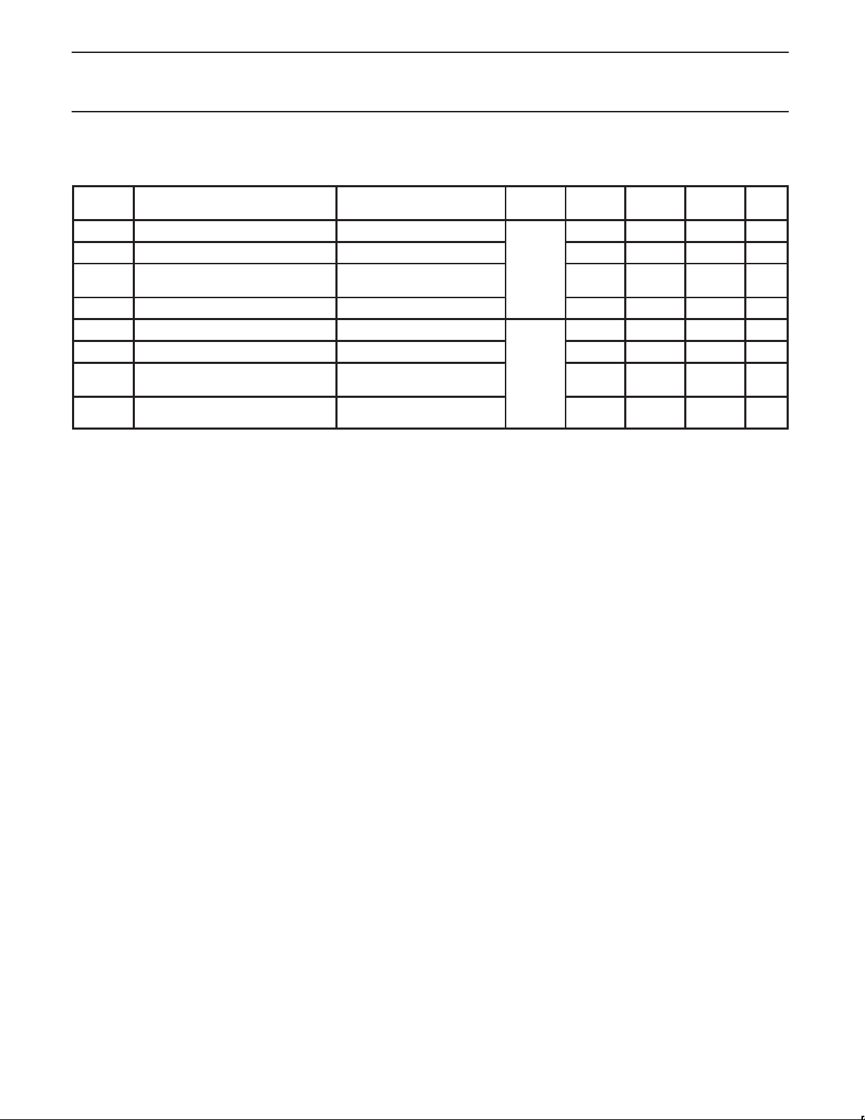
DC ELECTRICAL CHARACTERISTICS
Characteristics measured with T
SYMBOL
V
S
∆V
S
Reset detection threshold VS – 2% V
Hysteresis VDD = 0 V → VS + 1.0 V → 0 V
PARAMETER CONDITIONS
VS/∆T Threshold voltage temperature
coefficient
I
CC
I
OH
I
DS1
I
DS2
I
DS3
Supply current VDD = VS + 1.0 V – 0.25 1.0 µA
IDS leakage current when OFF VDD = VDS = 10 V – – 0.1 µA
N-channel IDS output sink current 1 VDS = 0.5 V; VDD = 1.2 V –0.23 –1.4 – mA
N-channel IDS output sink current 2
(for VS > 2.6 V)
N-channel IDS output sink current 3
(for V
> 3.9 V)
S
= 25 °C, unless otherwise specified.
amb
–40 °C ≤ T
VDS = 0.5 V; VDD = 2.4 V
VDS = 0.5 V; VDD = 3.6 V –3.2 –14.7 – mA
≤ +85 °C
amb
TEST
CIRCUIT
Fig. 17
2
Fig. 18
MIN. TYP. MAX. UNIT
VS + 2% V
S
VS × 0.03 VS × 0.05 VS × 0.08 V
– ±0.01 – %/°C
–1.6 –8.3 – mA
2001 Jun 19
4
 Loading...