

Philips NE556-1N, NE556-1F, SA556-1F, SA556N Datasheet

Philips Semiconductors Linear Products Product specification
NE/SA/SE556/NE556-1Dual timer
353
August 31, 1994 853-0035 13721
DESCRIPTION
Both the 556 and 556-1 Dual Monolithic timing circuits are highly
stable controllers capable of producing accurate time delays or
oscillation. The 556 and 556-1 are a dual 555. Timing is provided by
an external resistor and capacitor for each timing function. The two
timers operate independently of each other, sharing only V
CC
and
ground. The circuits may be triggered and reset on falling
waveforms. The output structures may sink or source 200mA.
FEATURES
•Turn-off time less than 2µs (556-1)
•Maximum operating frequency >500kHz (556-1)
•Timing from microseconds to hours
•Replaces two 555 timers
•Operates in both astable and monostable modes
•High output current
•Adjustable duty cycle
•TTL compatible
•Temperature stability of 0.005%/°C
•SE556-1 compliant to MIL-STD or JAN
APPLICATIONS
•Precision timing
•Sequential timing
•Pulse shaping
PIN CONFIGURATION
D, F, N Packages
1
2
3
4
5
6
7 8
14
13
12
11
10
9
DISCHARGE
THRESHOLD
CONTROL VOLTAGE
RESET
OUTPUT
TRIGGER
GND
V
CC
DISCHARGE
THRESHOLD
CONTROL VOLTAGE
RESET
OUTPUT
TRIGGER
•Pulse generator
•Missing pulse detector
•Tone burst generator
•Pulse width modulation
•Time delay generator
•Frequency division
•Touch-Toneencoder
•Industrial controls
•Pulse position modulation
•Appliance timing
•Traffic light control
BLOCK DIAGRAM
DISCHARGE
THRESHOLD
CONTROL VOLTAGE
RESET
OUTPUT
TRIGGER
GROUND
V
CC
DISCHARGE
THRESHOLD
CONTROL VOLTAGE
RESET
OUTPUT
TRIGGER
COMP
FLIP FLOP
COMP
COMP
FLIP FLOP
COMP
1
2
3
4
5
6
7
14
13
12
11
10
9
8
Touch-Tone is a registered trademark of AT&T
Philips Semiconductors Linear Products Product specification
NE/SA/SE556/NE556-1Dual timer
August 31, 1994
354
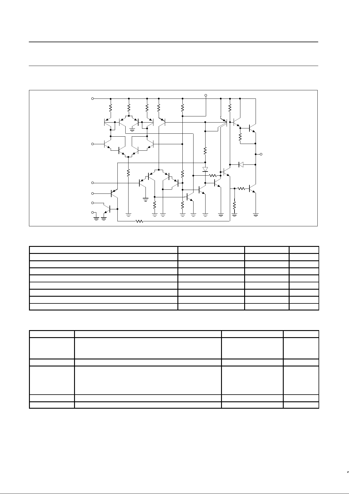
EQUIVALENT SCHEMATIC (Shown for one circuit only)
R3
4.7K
CB
Q18
E
R9
5K
R6
100K
V
CC
R1
4.7K
R2
330
R4
1K
Q5 Q6 Q7
Q9
Q8
R7
5K
R12
6.8K
Q19
Q21
R13
3.3K
Q22
OUTPUT
Q23
C B
Q20
R14
220
Q24
Q17
R11
4.7K
R10
3.2
K
Q16
R8
5K
Q15
Q11 Q12
Q10 Q13
R5
10K
R15
4.7K
R16
100
Q25
Q14
Q2 Q3
Q1
Q4
CONTROL VOLTAGE
THRESHOLD
TRIGGER
RESET
DISCHARGE
GND
ORDERING INFORMATION
DESCRIPTION TEMPERATURE RANGE ORDER CODE DWG #
14-Pin Plastic Small Outline (SO) Package 0 to +70°C NE556D 0175D
14-Pin Ceramic Dual In-Line Package (CERDIP) 0 to +70°C NE556F 0581B
14-Pin Plastic Dual In-Line Package (DIP) 0 to +70°C NE556N 0405B
14-Pin Ceramic Dual In-Line Package (CERDIP) 0 to +70°C NE556-1F 0581B
14-Pin Plastic Dual In-Line Package (DIP) 0 to +70°C NE556-1N 0405B
14-Pin Plastic Dual In-Line Package (DIP) -40°C to +85°C SA556N 0405B
14-Pin Ceramic Dual In-Line Package (CERDIP) -55°C to +125°C SE556F 0581B
14-Pin Plastic Dual In-Line Package (DIP) -55°C to +125°C SE556N 0405B
ABSOLUTE MAXIMUM RATINGS
SYMBOL PARAMETER RATING UNIT
V
CC
Supply voltage
NE/SA556, NE556-1 +16 V
SE556 +18 V
P
D
Maximum allowable power dissipation
1
800 mW
T
A
Operating temperature range
NE556-1, NE556 0 to +70 °C
SA556 -40 to +85 °C
SE556 -55 to +125 °C
T
STG
Storage temperature range -65 to +150 °C
T
SOLD
Lead soldering temperature (10sec max) +300 °C
NOTES:
1. The junction temperature must be kept below 125°C for the D package and below 150°C for the N and F packages. At ambient temperatures
above 25°C, where this limit would be exceeded, the Maximum Allowable Power Dissipation must be derated by the following:
D package 115°C/W
N package 80°C/W
F package 100°C/W
 Loading...