

Philips NE5521D, NE5521N, SA5521D, SA5521N Datasheet
Philips Semiconductors Linear Products Product specification
NE/SA/SE5521LVDT signal conditioner
901
August 31, 1994 853-0043 13721
DESCRIPTION
The NE/SA/SE5521 is a signal conditioning circuit for use with
Linear Variable Differential Transformers (LVDTs) and Rotary
Variable Differential Transformers (RVDTs). The chip includes a low
distortion, amplitude-stable sine wave oscillator with programmable
frequency to drive the primary of the LVDT/RVDT, a synchronous
demodulator to convert the LVDT/RVDT output amplitude and phase
to position information, and an output amplifier to provide
amplification and filtering of the demodulated signal.
FEATURES
•Low distortion
•Single supply 5V to 20V, or dual supply ±2.5V to ±10V
•Oscillator frequency 1kHz to 20kHz
•Capable of ratiometric operation
•Low power consumption (182mV typ)
APPLICATIONS
•LVDT signal conditioning
•RVDT signal conditioning
•LPDT signal conditioning
•Bridge circuits
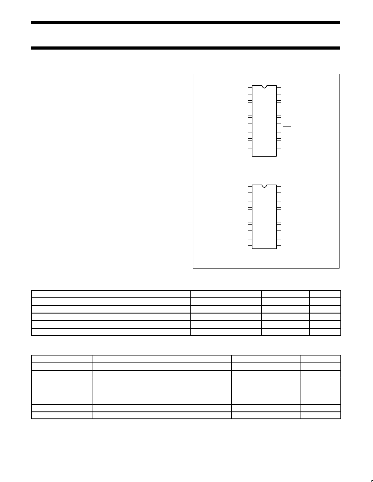
PIN CONFIGURATIONS
1
2
3
4
5
6
7
8
9
10
11
12
13
14
16
15
1
2
3
4
5
6
7
8
11
12
13
14
15
16
18
17
9
10
AMP OUT
+IN
–IN
LVDT IN
DEMOD OUT
SYNC
GND
N.C.
N.C.
V+
C
T
V
REF
FEEDBACK
OSC
OSC
V
REF/2
R
T
N.C.
AMP OUT
+IN
–IN
LVDT IN
DEMOD OUT
SYNC
GND
N.C.
V+
C
T
V
REF
FEEDBACK
OSC
OSC
V
REF/2
R
T
F, N Packages
TOP VIEW
D1 Package
TOP VIEW
NOTE:
1. SOL — released in large SO package only.
ORDERING INFORMATION
DESCRIPTION TEMPERATURE RANGE ORDER CODE DWG #
18-Pin Plastic Dual In-Line Package (DIP) 0 to +70°C NE5521N 0407A
16-Pin Small Outline Large (SOL) Package 0 to +70°C NE5521D 0171B
18-Pin Plastic Dual In-Line Package (DIP) –40 to +85°C SA5521N 0407A
18-Pin Ceramic Dual In-Line Package (CERDIP) –55 to +125°C SE5521F 0583A
16-Pin Ceramic Dual In-Line Package (CERDIP) –40 to +85°C SA5521D 0582B
ABSOLUTE MAXIMUM RATINGS
SYMBOL PARAMETER RATING UNIT
V
CC
Supply voltage +20 V
Split supply voltage ±10 V
T
A
Operating temperature range
NE5521
SA5521
SE5521
0 to 70
–40 to +85
–55 to +125
°C
°C
°C
T
STG
Storage temperature range –65 to +125 °C
P
D
Power dissipation
1
910 mW
NOTES:
1. For derating, see typical power dissipation versus load curves (Figure 1).
Philips Semiconductors Linear Products Product specification
NE/SA/SE5521LVDT signal conditioner
August 31, 1994
902
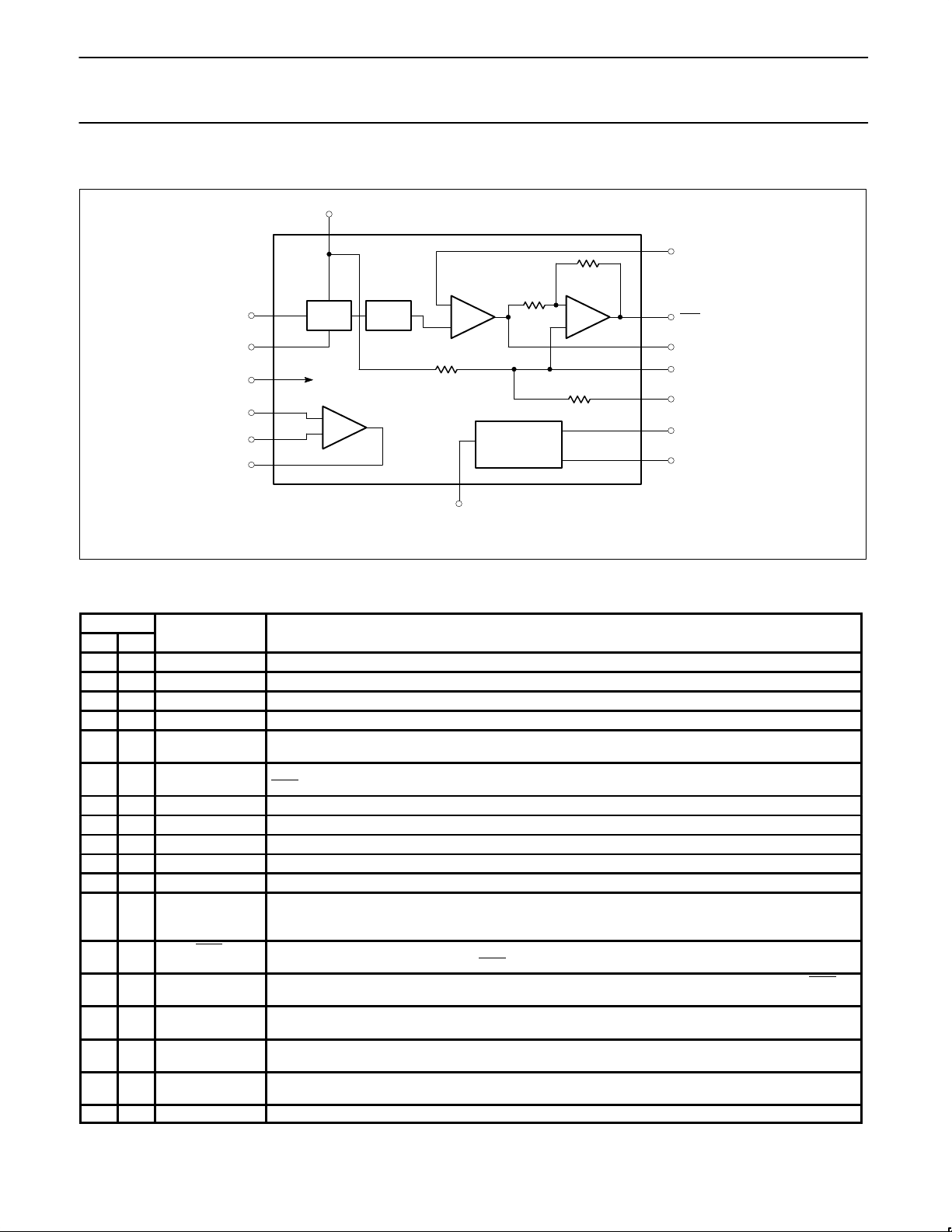
BLOCK DIAGRAM
NOTE:
Pin numbers are for F, N packages.
16
17
11
18
3
2
1
5
15
13
14
12
7
4
6
OSC
AUX AMP
DOMOD OUT
SINE
CONV
10k
10k
10k
10k
–
+
FEEDBACK
OSC
GND/V–
LVDT IN
SYNC
–
+
–
+
V
REF
V
REF
/2
OSC
C
T
R
T
V+
–IN
+IN
AMP
OUT
SYNCHRONOUS
DEMODULATOR
PIN DEFINITIONS FOR D, F AND N PACKAGES
PIN NO.
D F, N
SYMBOL
DEFINITION
1 1 Amp Out Auxiliary Amplifier Out.
2 2 +IN Auxiliary Amplifier non-inverting input.
3 3 –IN Auxiliary Amplifier inverting input.
4 4 LVDT IN Input to Synchronous Demodulator from the LVDT/RVDT secondary.
5 5 DEMOD OUT Pulsating DC output from the Synchronous Demodulator output. This voltage should be filtered before
use.
6 6 SYNC Synchronizing input for the Synchronizing Demodulator. This input should be connected to the OSC or
OSC
output. Sync is referenced to V
REF
/2.
7 7 GND Device return. Should be connected to system ground or to the negative supply.
8 8 NC No internal connection.
-- 9 NC No internal connection.
-- 10 NC No internal connection.
9 11 R
T
A temperature stable 18kΩ resistor should be connected between this pin and Pin 7.
10 12 V
REF
/2 A high impedance source of one half the potential applied to V
REF
. The LVDT/RVDT secondary return
should be to this point. A bypass capacitor with low impedance at the oscillator frequency should also be
connected between this pin and ground.
11 13 OSC Oscillator sine wave output that is 180° out of phase with the OSC signal. The LVDT/RVDT primary is
usually connected between OSC and OSC
pins.
12 14 OSC Oscillator sine wave output. The LVDT/RVDT primaries are usually connected between OSC and OSC
pins.
13 15 FEEDBACK Usually connected to the OSC output for unity gain, a resistor between this pin and OSC, and one be-
tween this pin and ground can provide for a change in the oscillator output pin amplitudes.
14 16 V
REF
Reference voltage input for the oscillator and sine converter. This voltage MUST be stable and must not
exceed +V supply voltage.
15 17 C
T
Oscillator frequency-determining capacitor. The capacitor connected between this pin and ground should
be a temperature-stable type.
16 18 +V Positive supply connection.
 Loading...