


INTEGRATED CIRCUITS
SA3601
Low voltage dual-band RF front-end
Preliminary specification 1999 Nov 09

Philips Semiconductors Preliminary specification
TYPE NUMBER
SA3601Low voltage dual-band RF front-end
DESCRIPTION
The SA3601 is an integrated dual-band RF front-end that operates at
both cellular (AMPS and TDMA) and PCS (TDMA) frequencies, and
is designed in a 20 GHz f
BiCMOS process—QUBiC2. The
T
low-band (LB) receiver is a combined low-noise amplifier (LNA) and
mixer. The LNA has a 1.7 dB noise figure (NF) at 881 MHz with 17 dB
of gain and an IIP3 of –7 dBm. The wide-dynamic range mixer has a
9.5 dB NF at 881 MHz with 9.5 dB of gain and an IIP3 of +6 dBm.
The high-band (HB) receiver is a combined low-noise amplifier (LNA)
and mixer, with the low-band and high-band mixers sharing the same
mixer output. The LNA has a 2.2 dB NF at 1960 MHz with 16 dB of
gain and an IIP3 of –5 dBm. The wide-dynamic range mixer has a
8.5 dB NF at 1960 MHz with 8.5 dB of gain and an IIP3 of +5.5 dBm.
FEATURES
•Low current consumption: LB I
= 14 mA; HB ICC = 15.5 mA
CC
•Outstanding low- and high-band noise figure
•LNAs with gain control (30 dB gain step)
•LO input and output buffers
•Frequency doubler
•On chip logic for network selection and power down
•Very small outline package
APPLICATIONS
•800 to 1000 MHz analog and digital receivers
•1800 to 2000 MHz digital receivers
•Portable radios
•Mobile communications equipment
PIN CONFIGURATION
HBLNA_IN
GND
V
HBMXR+_IN
HBMXR–_IN
PD1
V
GND
GND
1
2
3
CC
4
5
6
7
CC
8
9
10 11 12 13 14 15 16
GND
HBLNA_OUT
TOP VIEW
GND
GND
LBLNA_OUT
26272829303132
GND
LBLNA_IN
25
24
23
22
21
20
19
18
17
GND
V
CC
LBMXR_IN
GND
MXR+_OUT
MXR–_OUT
GND
LBVCO_IN
PD2
GND
GND
LBVCO_OUT
GND
PD3
HBVCO_IN
GND
ORDERING INFORMATION
PACKAGE
NAME DESCRIPTION VERSION
SA3601 BCC32++ HBCC32: plastic, heatsink bottom chip carrier; 32 terminals; body 5 x 5 x 0.65 mm SOT560-1
SR02237
1999 Nov 09
2
Philips Semiconductors Preliminary specification
SA3601Low voltage dual-band RF front-end
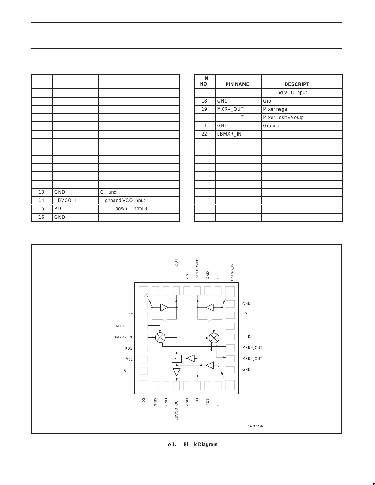
PIN DESCRIPTIONS
PIN
NO.
PIN NAME DESCRIPTION
1 HBLNA_IN Highband LNA input
2 GND Ground
3 V
CC
Power supply
4 HBMXR+_IN Highband mixer positive input
5 HBMXR–_IN Highband mixer negative input
6 PD1 Power down control 1
7 V
CC
Power supply
8 GND Ground
9 PD2 Power down control 2
10 GND Ground
11 GND Ground
12 LBVCO_OUT Lowband VCO buffered output
13
14
15
16
GND
HBVCO_IN
PD3
GND
Ground
Highband VCO input
Power down control 3
Ground
PIN
NO.
PIN NAME DESCRIPTION
17 LBVCO_IN Lowband VCO input
18 GND Ground
19 MXR–_OUT Mixer negative output
20 MXR+_OUT Mixer positive output
21 GND Ground
22 LBMXR_IN Lowband mixer input
23 V
CC
Power supply
24 GND Ground
25 LBLNA_IN Lowband LNA input
26 GND Ground
27 GND Ground
28 LBLNA_OUT Lowband LNA output
29
30
31
32
GND
HBLNA_OUT
GND
GND
Ground
Highband LNA output
Ground
Ground
BLOCK DIAGRAM
HBLNA_IN
GND
V
HBMXR+_IN
HBMXR–_IN
PD1
V
GND
GND
GND
1
2
CC
3
4
5
6
7
CC
8
9
10 11 12 13 14 15 16
PD2
GND
GND
HBLNA_OUT
TOP VIEW
x2
LBVCO_OUT
GND
GND
GND
LBLNA_OUT
PD3
HBVCO_IN
26272829303132
GND
GND
25
24
23
22
21
20
19
18
17
LBLNA_IN
GND
V
LBMXR_IN
GND
MXR+_OUT
MXR–_OUT
GND
LBVCO_IN
CC
SR02238
1999 Nov 09
Figure 1. Block Diagram
3
Philips Semiconductors Preliminary specification
SA3601Low voltage dual-band RF front-end
MODE SELECT LOGIC
PD1 PD2 PD3 OPERATING MODE
0 0 0 Sleep mode off off off off off off off
0 0 1 Tx mode, LO lowband buffer off off off off off on off
0 1 0 Rx mode cellular, low gain off on off off off on off
0 1 1 Rx mode cellular, high gain on on off off off on off
1 0 0 Rx mode PCS, low gain, x2 off off off on on on off
1 0 1 Rx mode PCS, high gain, x2 off off on on on on off
1 1 0 Rx mode PCS, low gain, no x2 off off off on off off off
1 1 1 Rx mode PCS, high gain, no x2 off off on on off off off
Cel
LNA
Cel
MXR
PCS
LNA
PCS
MXRx2DBL
LB LO
O/P
HB LO
O/P
1999 Nov 09
4

Philips Semiconductors Preliminary specification
SA3601Low voltage dual-band RF front-end
OPERA TION
The SA3601 is a highly integrated dual-band radio frequency (RF)
front-end integrated circuit (IC) targeted for TDMA applications. This
IC is split into separate low-band (LB) and high-band (HB) receivers.
The LB receiver contains a low noise amplifier (LNA) and mixer that
are designed to operate in the cellular frequency range
(869–894MHz). The HB receiver contains an LNA and mixer that
are designed to operate in the PCS frequency range
(1930–1990 MHz). The SA3601 also contains a frequency doubler
that can drive the HB mixer local oscillator (LO) port, allowing a
single-band voltage controlled oscillator (VCO) to be used to drive
both mixers. Modes for bypassing the doubler are also provided, in
the case where a dual-band VCO is used.
The SA3601 has eight modes of operation that control the LNAs,
mixers, LO buffers and doubler . The select pins (PD1,2,3) are used
to change modes of operation. The internal select logic powers the
device down (0,0,0), turns on the LB LO buffer for use in transmit
mode (0,0,1), enables cellular receive mode for high and low gain
(0,1,X), enables PCS receive mode for high and low gain both
without doubler (1,1,X) and with doubler (1,0,X).
Low-Band Receive Section
The LB circuit contains a LNA followed by a wide dynamic range
active mixer. In a typical application circuit, the LNA output uses an
external pull-up inductor to VCC and is AC coupled. The mixer IF
outputs are differential and are combined with the high-band IF
mixer outputs thereby eliminating the need for extra output pins.
External inductors and capacitors can be used to convert the
differential mixer outputs to single-ended. Furthermore, the LNA
provides two gain settings: high gain (17dB) and low gain (–15 dB).
The desired gain state can be selected by setting the logic pins
(PD1,PD2,PD3) appropriately.
High-Band Receive Section
The HB circuit contains a LNA followed by a Gilbert cell mixer with
differential inputs. The LNA output uses an internal pull-up inductor
to VCC , which eliminates the need for an external pull-up. The
mixer IF outputs are differential and are combined with the low-band
IF mixer outputs thereby eliminating the need for extra output pins.
Similar to the LB LNA, the HB LNA has two gain settings: high gain
(16 dB) and low gain (–15 dB).
Control Logic Section
Pins PD1, PD2, and PD3, control the logic functions of the SA3601.
The PD1 selects between LB and HB operations. In LB receive
mode, the LB LNA is in high gain mode (or on) when PD1,2,3 are
(0,1,1). In all other modes, the LB LNA is off. The LB mixer is on
when PD1,2,3 are (0,1,X). In all other modes, the LB mixer is off.
During transmit mode when PD1,2,3 are (0,0,1), the LB LO buffer is
on, enabling use of the LO signal for the transmitter.
In HB receive mode, the HB LNA is in high gain mode (or on) when
PD1,2,3 are (1,X,1). In all other modes, the HB LNA is off. The HB
mixer is on when PD1,2,3 are (1,X,X), and is off in all other modes.
The on-chip frequency doubler (X2) is on in (1,0,X) modes. When
the frequency doubler is on, the input signal from the LB LO buffer is
doubled in frequency, which can then be used to drive the HB mixer
LO port. The frequency doubler can also be bypassed in modes
(1,1,X), in which case the HB mixer is driven directly by an external
2 GHz LO signal.
1999 Nov 09
5
 Loading...