

Philips SA3600 Datasheet

INTEGRATED CIRCUITS
SA3600
Low voltage dual-band RF front-end
Product specification
Supersedes data of 1999 March 18
1999 Nov 02
Philips Semiconductors Product specification
TYPE NUMBER
SA3600Low voltage dual-band RF front-end
DESCRIPTION
The SA3600 is an integrated dual-band RF front-end that operates at
both cellular (AMPS and TDMA) and PCS (TDMA) frequencies, and
is designed in a 20 GHz f
BiCMOS process—QUBiC2.
T
The low-band (LB) receiver is a combined low-noise amplifier (LNA)
and mixer. The LNA has a 1.7 dB noise figure (NF) at 881 MHz with
17 dB of gain and an IIP3 of –7 dBm. The wide-dynamic range mixer
has a 9.5 dB NF at 881 MHz with 9.5 dB of gain and an IIP3 of
+6 dBm.
The high-band (HB) receiver is a combined low-noise amplifier (LNA)
and mixer, with the low-band and high-band mixers sharing the same
mixer output. The LNA has a 2.2 dB NF at 1960 MHz with 16 dB of
gain and an IIP3 of –5 dBm. The wide-dynamic range mixer has a 8.5
dB NF at 1960 MHz with 8.5 dB of gain and an IIP3 of +5.5 dBm.
FEATURES
•Low current consumption: LB I
= 14.5 mA; HB ICC = 20.5 mA
CC
•Outstanding low- and high-band noise figure
•LNAs with gain control (30 dB gain step)
•LO input and output buffers
•Selectable frequency doubler
•On chip logic for network selection and power down
•Very small outline package
APPLICATIONS
•800 to 1000 MHz analog and digital receivers
•1800 to 2000 MHz digital receivers
•Portable radios
•Mobile communications equipment
PIN CONFIGURATION
HB_LNA_OUT
GND
HB_LNA_IN
V
HB_MXR+_IN
HB_MXR–_IN
PD1
GND
HB_VCO_OUT
PD2
GND
LB_VCO_OUT
1
2
3
4
CC
5
6
7
8
9
10
11
12 13
LB_LNA_OUT
24
23
GND
22
LB_LNA_IN
21
V
CC
20
LB_MXR_IN
19
GND
18
MXR+_OUT
17
MXR–_OUT
16
GND
15
LB_VCO_IN
PD3
14
HB_VCO_IN
SR01596
ORDERING INFORMA TION
PACKAGE
NAME DESCRIPTION VERSION
SA3600 TSSOP24 Plastic thin shrink small outline package; 24 leads; body width 4.4 mm SOT355–1
PIN DESCRIPTIONS
PIN
NO.
PIN NAME DESCRIPTION
1 HB_LNA_OUT Highband LNA output 13 HB_VCO_IN Highband VCO input
2 GND Ground 14 PD3 Power down control 3
3 HB_LNA_IN Highband LNA input 15 LB_VCO_IN Lowband VCO input
4 Vcc Power supply 16 GND Ground
5 HB_MXR+_IN Highband mixer positive input 17 MXR–_OUT Mixer negative output
6 HB_MXR–_IN Highband mixer negative input 18 MXR+_OUT Mixer positive output
7 PD1 Power down control 1 19 GND Ground
8 GND Ground 20 LB_MXR_IN Lowband mixer input
9 HB_VCO_OUT Highband VCO buffered output 21 V
10 PD2 Power down control 2 22 LB_LNA_IN Lowband LNA input
11 GND Ground 23 GND Ground
12 LB_VCO_OUT Lowband VCO buffered output 24 LB_LNA_OUT Lowband LNA output
PIN
NO.
PIN NAME DESCRIPTION
CC
Power supply
1999 Nov 02 853–2183 22617
2
Philips Semiconductors Product specification
SA3600Low voltage dual-band RF front-end
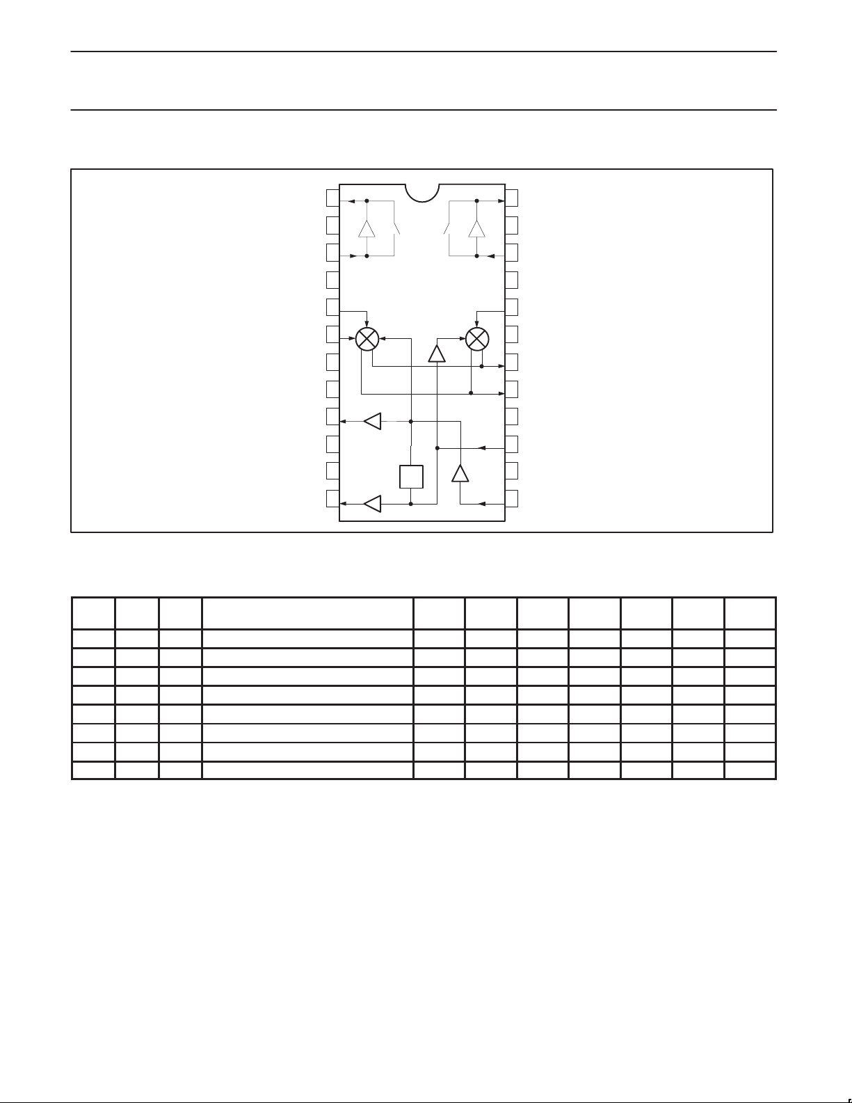
BLOCK DIAGRAM
LB_LNA_OUT
24
23
GND
22
LB_LNA_IN
21
V
CC
20
LB_MXR_IN
19
GND
18
MXR+_OUT
17
MXR–_OUT
16
GND
15
LB_VCO_IN
14
PD3
HB_VCO_IN
SR01594
HB_LNA_OUT
GND
HB_LNA_IN
V
HB_MXR+_IN
HB_MXR–_IN
PD1
GND
HB_VCO_OUT
PD2
GND
LB_VCO_OUT
1
2
3
4
CC
5
6
7
8
9
10
11
12 13
SA3600
x2
Figure 1. Block Diagram
MODE SELECT LOGIC
PD1 PD2 PD3 OPERATING MODE
0 0 0 Sleep mode off off off off off off off
0 0 1 Tx mode, LO lowband buffer off off off off off on off
0 1 0 Rx mode cellular, low gain off on off off off on off
0 1 1 Rx mode cellular, high gain on on off off off on off
1 0 0 Rx mode PCS, low gain, x2 off off off on on on off
1 0 1 Rx mode PCS, high gain, x2 off off on on on on off
1 1 0 Rx mode PCS, low gain, no x2 off off off on off off on
1 1 1 Rx mode PCS, high gain, no x2 off off on on off off on
Cel
LNA
Cel
MXR
PCS
LNA
PCS
MXRx2DBL
LB LO
O/P
HB LO
O/P
1999 Nov 02
3

Philips Semiconductors Product specification
SA3600Low voltage dual-band RF front-end
OPERA TION
The SA3600 is a highly integrated dual-band radio frequency (RF)
front-end integrated circuit (IC) targeted for TDMA applications. This
IC is split into separate low-band (LB) and high-band (HB) receivers.
The LB receiver contains a low noise amplifier (LNA) and mixer that
are designed to operate in the cellular frequency range
(869–894MHz). The HB receiver contains an LNA and mixer that
are designed to operate in the PCS frequency range
(1930–1990 MHz). The SA3600 also contains a frequency doubler
that can drive the HB mixer local oscillator (LO) port, allowing a
single-band voltage controlled oscillator (VCO) to be used to drive
both mixers. Modes for bypassing the doubler are also provided, in
the case where a dual-band VCO is used.
The SA3600 has eight modes of operation that control the LNAs,
mixers, LO buffers and doubler . The select pins (PD1,2,3) are used
to change modes of operation. The internal select logic powers the
device down (0,0,0), turns on the LB LO buffer for use in transmit
mode (0,0,1), enables cellular receive mode for high and low gain
(0,1,X), enables PCS receive mode for high and low gain both
without doubler (1,1,X) and with doubler (1,0,X).
Low-Band Receive Section
The LB circuit contains a LNA followed by a wide dynamic range
active mixer. In a typical application circuit, the LNA output uses an
external pull-up inductor to VCC and is AC coupled. The mixer IF
outputs are differential and are combined with the high-band IF
mixer outputs thereby eliminating the need for extra output pins.
External inductors and capacitors can be used to convert the
differential mixer outputs to single-ended. Furthermore, the LNA
provides two gain settings: high gain (17dB) and low gain (–15 dB).
The desired gain state can be selected by setting the logic pins
(PD1,PD2,PD3) appropriately.
High-Band Receive Section
The HB circuit contains a LNA followed by a Gilbert cell mixer with
differential inputs. The LNA output uses an internal pull-up inductor
to VCC , which eliminates the need for an external pull-up. The
mixer IF outputs are differential and are combined with the low-band
IF mixer outputs thereby eliminating the need for extra output pins.
Similar to the LB LNA, the HB LNA has two gain settings: high gain
(16 dB) and low gain (–15 dB).
Control Logic Section
Pins PD1, PD2, and PD3, control the logic functions of the SA3600.
The PD1 selects between LB and HB operations. In LB receive
mode, the LB LNA is in high gain mode (or on) when PD1,2,3 are
(0,1,1). In all other modes, the LB LNA is off. The LB mixer is on
when PD1,2,3 are (0,1,X). In all other modes, the LB mixer is off.
During transmit mode when PD1,2,3 are (0,0,1), the LB LO buffer is
on, enabling use of the LO signal for the transmitter.
In HB receive mode, the HB LNA is in high gain mode (or on) when
PD1,2,3 are (1,X,1). In all other modes, the HB LNA is off. The HB
mixer is on when PD1,2,3 are (1,X,X), and is off in all other modes.
The on-chip frequency doubler (X2) is on in (1,0,X) modes. When
the frequency doubler is on, the input signal from the LB LO buffer is
doubled in frequency, which can then be used to drive the HB mixer
LO port. The frequency doubler can also be bypassed in modes
(1,1,X), in which case the HB mixer is driven directly by an external
2 GHz LO signal.
Local Oscillator (LO) Section
The LB LO buffers are on for all modes except sleep mode, when
PD1,2,3 are (0,0,0), and for HB receive mode without doubler,
PD1,2,3 are (1,1,X). The HB LO buffers are on only when PD1,2,3
are (1,1,X). The PD1,2,3 pins are used to power-up/down all LO
input buffers, which minimizes the pulling effect on the external VCO
when entering receive or transmit mode.
1999 Nov 02
4
Philips Semiconductors Product specification
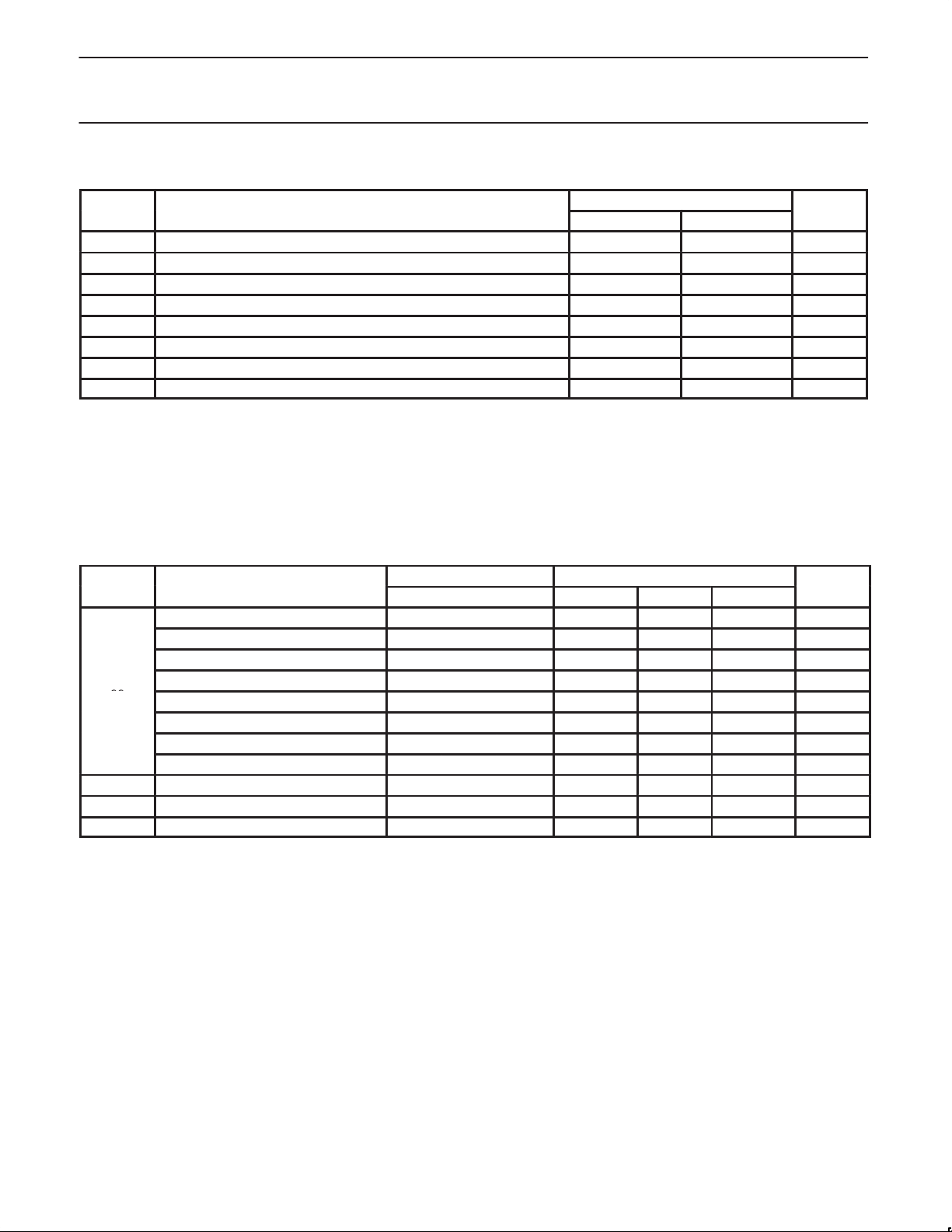
SYMBOL
PARAMETER
UNITS
SYMBOL
PARAMETER
UNIT
I
SA3600Low voltage dual-band RF front-end
ABSOLUTE MAXIMUM RATINGS
V
V
P
T
P
I
MAX
T
T
CC
IN
D
J MAX
MAX
STG
O
Supply voltage –0.3 +4.5 V
Voltage applied to any other pin –0.3 VCC+0.3 V
Power dissipation, T
amb
Maximum junction temperature 150 °C
Power input/output +20 dBm
DC current into any I/O pin –10 +10 mA
Storage temperature range –65 +150 °C
Operating temperature –40 +85 °C
1
= +25 °C (still air) 555 mW
NOTES:
1. IC is protected against ESD voltages up to 500 V (human body model).
DC ELECTRICAL CHARACTERISTICS
Unless otherwise specified, all Input/Output ports are single-ended.
DC PARAMETERS
V
CC
= +3.0 V, T
CC
V
IH
V
IL
I
BIAS
= +25°C unless otherwise specified
amb
TEST CONDITIONS TESTER LIMITS
PD1 PD2 PD3 MIN TYP MAX
Sleep mode 0 0 0 0.1 1 µA
Tx mode, LO lowband buffer 0 0 1 4.3 5.5 mA
Rx mode cellular, low gain 0 1 0 10.1 12 mA
Rx mode cellular, high gain 0 1 1 14 16.5 mA
Rx mode PCS, low gain, x2 1 0 0 17.5 21 mA
Rx mode PCS, high gain, x2 1 0 1 23.5 28 mA
Rx mode PCS, low gain, no x2 1 1 0 14.5 17.5 mA
Rx mode PCS, high gain, no x2 1 1 1 20.5 24.5 mA
Input HIGH voltage 0.5xV
Input LOW voltage –0.3 0.2xV
Input bias current Logic 1 or logic 0 –5 +5 µA
LIMITS
MIN. MAX.
CC
VCC+0.3 V
CC
V
1999 Nov 02
5
Philips Semiconductors Product specification
SYMBOL
PARAMETER
TEST CONDITIONS
UNIT
SA3600Low voltage dual-band RF front-end
AC ELECTRICAL CHARACTERISTICS
V
= +3.0 V, fRF = 881 MHz, fLO = 963 MHz, T
CC
Cascaded Gain Section
G
SYS
G
BYP
LB LNA + Mixer, High Gain Filter loss = 3 dB 20.5 23.5 26.5 dB
LB LNA + Mixer, Low Gain Filter loss = 3 dB –11.5 –8.5 –5.5 dB
Low-band LNA Section
f
G
NF
IIP3
P1dB
G
NF
IIP3
Z
Z
OUT
T
RF
ENA
ENA
BYP
BYP
IN
SW
RF input frequency range 869 894 MHz
Small signal gain ENABLED 16.1 17 17.9 dB
Noise figure ENABLED 1.5 1.7 1.9 dB
Input 3rd order Intercept Point –8.1 –7 –5.9 dBm
ENA
Input 1 dB Compression Point –20 dBm
ENA
Small signal gain BYPASSED –15 dB
Noise figure BYPASSED 15 dB
Input 3rd order Intercept Point 15 dBm
BYP
Input return loss
Output return loss
ENABLE/DISABLE speed
2
2
1
Low-band Mixer Section
f
f
G
NF
IIP3
P1dB
P
Z
Z
OUT
RF
f
IF
LO
MXR
MXR
LO
IN
RF input frequency range 869 894 MHz
IF output frequency range 70 200 MHz
LO input range 939 1100 MHz
Small signal gain PLO = –5 dBm 9 9.5 10 dB
SSB Noise figure PLO = –5 dBm 8.6 9.5 10.4 dB
Input 3rd order Intercept Point PLO = –5 dBm 5.1 6 6.9 dBm
MXR
Input 1 dB Compression Point P
MXR
LO input power range –7 –5 –3 dBm
Input return loss
Output return loss
2
2
Two-tone spurious rejection: PLO = –5 dBm
2-Tone
2(fRF–fTx), fRF–fTx=fIF/2
3(fRF–fTx), fRF–fTx=fIF/3
RF–LO RF to LO isolation 25 dB
LO–RF LO to RF isolation 40 dB
T
SW
ENABLE/DISABLE speed
1
Low-band LO Buffer Section
P
Z
P
P
OUT
Z
OUT
LO
IN
LO Input frequency range 939 1100 MHz
LO Input power 50 Ω matched LB_VCO_IN –7 –5 –3 dBm
IN
LO Output power 50 Ω matched LB_VCO_OUT –8 –7.5 –7 dBm
Input return loss
Output return loss
2
2
Harmonic content PLO = –5 dBm –20 dBc
T
SW
ENABLE/DISABLE speed
1
= +25°C, unless otherwise specified
amb
50 Ω system 10 dB
50 Ω system 10 dB
= –5 dBm –14 dBm
LO
50 Ω system 10 dB
50 Ω system 10 dB
fRF=890.0 MHz @–36 dBm
fTx=848.9 MHz @–20 dBm
fRF=876.3 MHz @–36 dBm
fTx=848.9 MHz @–20 dBm
50 Ω system 10 dB
50 Ω system 10 dB
LIMITS
MIN. –3 σ TYP +3 σ MAX.
20 µs
–110
–110
20 µs
20 µs
dBm
1999 Nov 02
6

Philips Semiconductors Product specification
SYMBOL
PARAMETER
TEST CONDITIONS
UNIT
NF
IIP3
IF/2 rej
RF
dBm
SA3600Low voltage dual-band RF front-end
AC ELECTRICAL CHARACTERISTICS
V
= +3.0 V, fRF = 1960 MHz, fLO = 2042 MHz, T
CC
Cascaded Gain Section
G
SYS
G
BYP
HB LNA + Mixer, High Gain Filter loss = 3 dB 18.5 21.5 24.5 dB
HB LNA + Mixer, Low Gain Filter loss = 3 dB –12.5 –9.5 –6.5 dB
High-band LNA Section
f
G
NF
IIP3
P1dB
G
NF
IIP3
Z
Z
OUT
T
RF
ENA
ENA
BYP
BYP
IN
SW
RF input frequency range 1930 1990 MHz
Small signal gain ENABLED 15 16 17 dB
Noise figure ENABLED 1.9 2.2 2.5 dB
Input 3rd order Intercept Point –6.5 –5 –3.5 dBm
ENA
Input 1 dB Compression Point –14 dBm
ENA
Small signal gain BYPASSED –15 dB
Noise figure BYPASSED 15 dB
Input 3rd order Intercept Point 15 dBm
BYP
Input return loss
2
Output return loss 50 Ω system, ENA and BYP 10 dB
ENABLE/DISABLE speed
1
High-band Mixer Section
G
f
RF
f
IF
f
LO
MXR
RF input frequency range 1930 1990 MHz
IF output frequency range 70 200 MHz
LO input range 2000 2190 MHz
Small signal gain PLO = –5 dBm 7.8 8.5 9.2 dB
SSB Noise figure, doubler off PLO = –5 dBm 7.6 8.5 9.4 dB
MXR
SSB Noise figure, doubler on PLO = –5 dBm 8.1 9 9.9 dB
Input 3rd order Intercept Point, doubler off PLO = –5 dBm 4 5.5 7 dBm
MXR
Input 3rd order Intercept Point, doubler on PLO = –5 dBm 1.9 3 4.1 dBm
P1dB
Input 1 dB Compression Point PLO = –5 dBm –14 dBm
MXR
Half-IF spurious rejection
2(fRF–fLO), fRF–fLO=fIF/2, doubler off
.
Half-IF spurious rejection
IF/3 rej.
2(f
Third-IF spurious rejection
3(fRF–fLO), fRF–fLO=fIF/3
), fRF–fLO=fIF/2, doubler on
RF–fLO
Two-tone spurious rejection: PLO = –5 dBm,
2-tone
fRF–fTx, fRF–fTx=f
2(fRF–fTx), fRF–fTx=fIF/2
IF
3(fRF–fTx), fRF–fTx=fIF/3
Z
P
Z
OUT
LO
IN
LO input power range –7 –5 –3 dBm
Input return loss
Output return loss
2
2
RF–LO RF to LO isolation 40 dB
LO–RF LO to RF isolation 30 dB
T
SW
ENABLE/DISABLE speed
1
= +25°C, unless otherwise specified
amb
50 Ω system, ENA and BYP 10 dB
fRF=1972.0 MHz @–36 dBm
fLO=2013.1 MHz @–5 dBm
fRF=1985.7 MHz @–36 dBm
fLO=2013.1 MHz @–5 dBm
fRF=1933.0 MHz @–36 dBm
fTx=1850.8 MHz @–20 dBm
fRF=1951.0 MHz @–36 dBm
fTx=1909.9 MHz @–20 dBm
fRF=1937.3 MHz @–36 dBm
fTx=1909.9 MHz @–20 dBm
50 Ω system 10 dB
50 Ω system 10 dB
LIMITS
MIN. –3 σ TYP +3 σ MAX.
20 µs
–90
–85
–114 dBm
–70
–115
–125
20 µs
dBm
1999 Nov 02
7

Philips Semiconductors Product specification
SYMBOL
PARAMETER
TEST CONDITIONS
UNITS
SA3600Low voltage dual-band RF front-end
AC ELECTRICAL CHARACTERISTICS
VCC = +3.0 V, T
High-band LO Buffer Section
P
LO
P
IN
P
OUT
Z
IN
Z
OUT
T
SW
x2 LO Doubler Section
f
LO
P
IN
Z
IN
Z
OUT
T
SW
NOTES:
1. Dependent on external components.
2. External matching required.
= +25°C, unless otherwise specified
amb
LIMITS
MIN. –3 σ TYP +3 σ MAX.
LO Input frequency range 2000 2190 MHz
LO Input power 50 Ω matched HB_VCO_IN –7 –5 –3 dBm
LO Output power 50 Ω matched HB_VCO_OUT –8.8 –8 –7.2 dBm
Input return loss
Output return loss
2
2
50 Ω system 10 dB
50 Ω system 10 dB
Harmonic content PLO = –5 dBm –20 dBc
ENABLE/DISABLE speed
1
20 µs
LO Input frequency 1000 1095 MHz
LO Input power 50 Ω matched LB_VCO_IN –7 –5 –3 dBm
Input return loss
Output return loss
ENABLE/DISABLE speed
2
2
1
50 Ω system 10 dB
50 Ω system 10 dB
20 µs
1999 Nov 02
8
Philips Semiconductors Product specification
SA3600Low voltage dual-band RF front-end
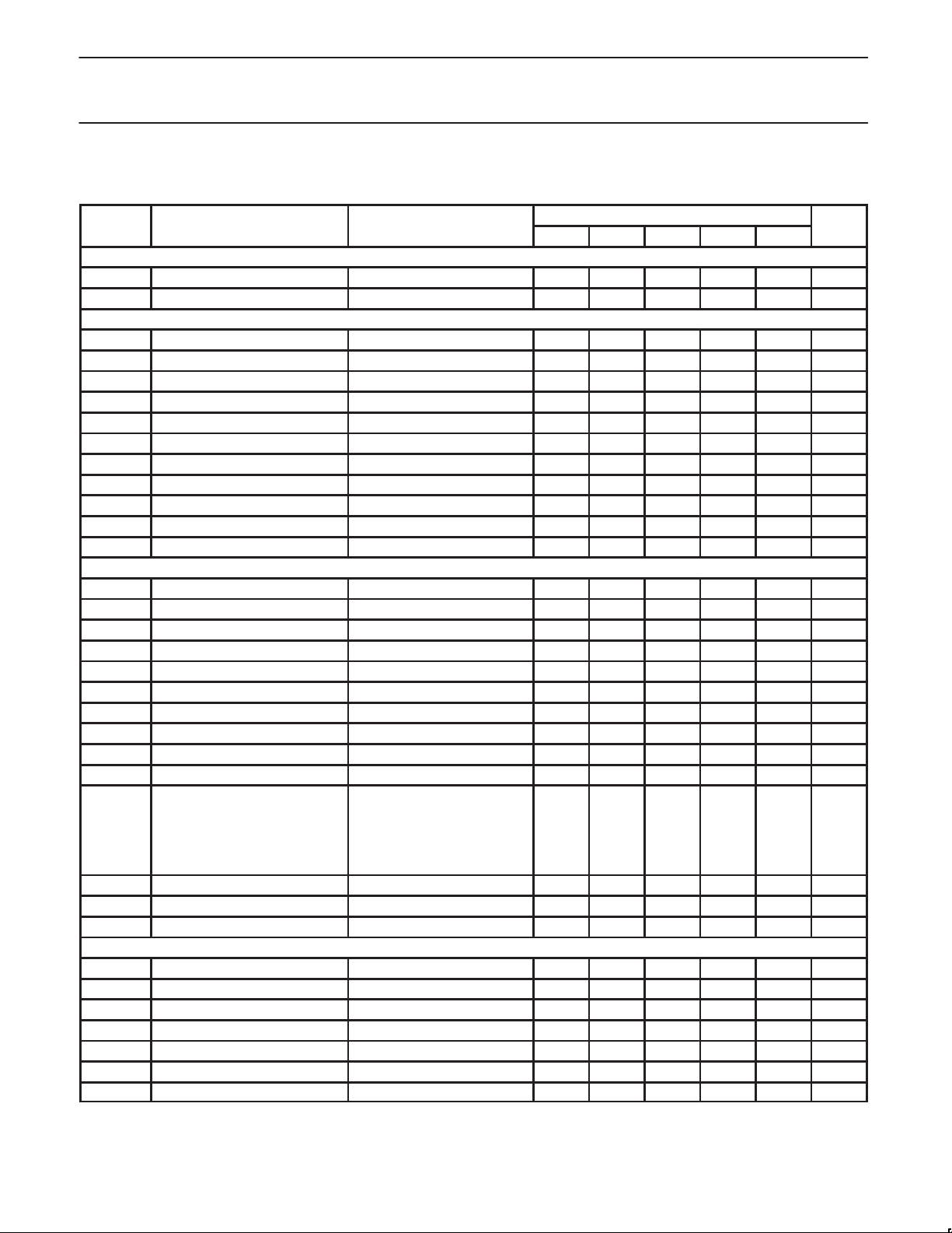
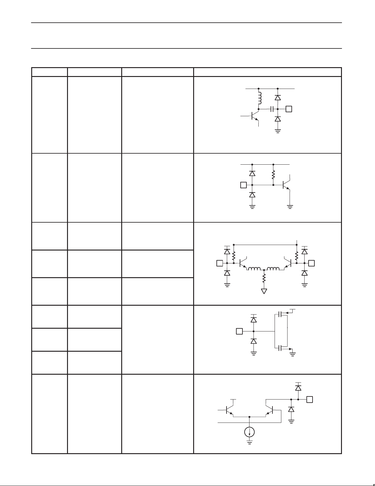
PIN NO
PIN MNEMONIC DC V EQUIVALENT CIRCUIT
1 HB LNA OUT
3 HB LNA IN 0.8
4 V
CC
V
CC
SR01786
V
BIAS
5K
SR01787
V
CC
V
BIAS
5 HB MXR+ IN 1.2
6 HB MXR– IN 1.2
7 PD1
10 PD2 Apply externally
14 PD3
9 HB VCO OUT Pull-up externally to V
CC
SR01788
SR01789
V
CC
V
CC
1999 Nov 02
SR01790
9
 Loading...