

Page 1
Colour Television Chassis
I_18020_000.eps
110908
ESSENCEESSENCE
Q529.1E
LC
Contents Page Contents Page
1. Technical Specifications, Connections, and Chassis
Overview 2
2. Safety Instructions, Warnings, and Notes 7
3. Directions for Use 8
4. Mechanical Instructions 9
5. Service Modes, Error Codes, and Fault Finding 24
6. Block Diagrams, Test Point Overview, and
Waveforms
Wiring Diagram Essence 57
Block Diagram Video 58
Block Diagram Audio 59
Block Diagram Control & Clock Signals 60
Test Point Overview SSB 61-66
I2C IC Overview 67
Supply Lines Overview 68
7. Circuit Diagrams and PWB Layouts Drawing PWB
SSB (B01-B09) 69-116 120-129
SSB: SRP List Explanation 117
SSB: SRP List Part 1 118
SSB: SRP List Part 2 119
I/O Panel (G) 130 131
IR & LED Panel (ME TOP) (J) 132 133
LVDS2DP Panel: Connector & Supply (LD1) 134 140-141
LVDS2DP Panel: FPGA: I/O Banks (LD2) 135 140-141
LVDS2DP Panel: Genesis (LD3) 136 140-141
LVDS2DP Panel: Fan Control (LD4) 137 140-141
LVDS2DP Panel: FPGA: Control (LD5) 138 140-141
LVDS2DP: SRP List 139
Monitor Panel: DC/DC (M01A) 142 151-152
Monitor Panel: DC/DC (M01B) 143 151-152
Monitor Panel: Audio (M02A) 144 151-152
Monitor Panel: Audio (M02B) 145 151-152
Monitor Panel: DP-Rx (M03A) 146 151-152
Monitor Panel: DP-Receiver & Power (M03B) 147 151-152
©
Copyright 2008 Koninklijke Philips Electronics N.V.
All rights reserved. No part of this publication may be reproduced, stored in a
retrieval system or transmitted, in any form or by any means, electronic,
mechanical, photocopying, or otherwise without the prior permission of Philips.
Monitor Panel: DP-Rx (M03C)148 151-152
Monitor Panel: DP-Rx (M03D)149 151-152
Monitor: SRP List 150
8. Alignments 153
9. Circuit Descriptions, Abbreviation List, and IC Data
Sheets 170
10. Spare Parts List & CTN Overview 185
11. Revision List 185
Published by EL 0872 BU TV Consumer Care Printed in the Netherlands Subject to modification EN 3122 785 18022
Page 2

EN 2 Q529.1E LC1.
Technical Specifications, Connections, and Chassis Overview
1. Technical Specifications, Connections, and Chassis Overview
Index of this chapter:
1.1 Technical Specifications
1.2 Connections
1.3 Chassis Overview
Notes:
• Figures can deviate due to the different set executions.
• Specifications are indicative (subject to change).
1.1 Technical Specifications
1.1.1 Vision
Display type : LCD
Screen size : 42" (107 cm), 16:9
Resolution (H × V pixels) : 1920 × 1080
Min. light output (cd/m
Min. contrast ratio : 66000:1
Max. response time (ms) : 2
Viewing angle (H × V degrees) : 176 × 176
Tuning system : PLL
TV Colour systems : PAL B/G, D/K, I
Video playback : NTSC, PAL, SECAM
Tuner bands : UHF, VHF, S, Hyper
Supported video formats
- 60 Hz : 480i
- 60 Hz : 480p
- 50 Hz : 576i
- 50 Hz : 576p
- 50, 60 Hz : 720p
- 50, 60 Hz : 1080i
- 24, 25, 30, 50, 60 Hz : 1080p
Supported computer formats:
- 60 Hz : 640 × 480
- 60 Hz : 800 × 600
- 60 Hz : 1024 × 768
- 60 Hz : 1280 × 768
- 60 Hz : 1360 × 768
- 60 Hz : 1920 × 1080i
- 60 Hz : 1920 × 1080p
Presets/channels : automatic channel
Tuner bands : VHF
2
) : 500
: SECAM B/G, D/K, L/L’
: DVB-T
: DVB-C (optional)
: MPEG4 (optional)
: UHF
: S-band
: Hyper-band
management
1.1.4 Miscellaneous
Power supply:
- Mains voltage (V
- Mains frequency (Hz) : 50 / 60
Ambient conditions:
- Temperature range (°C) : +5 to +35
Power consumption (values are indicative)
- Normal operation (W) : ≈248
- Standby (W) : < 0.40
Hub dimensions (W × H × D in mm) : 320 × 84 × 320
Hub weight (kg) : 4.7
Screen dimensions (W × H × D in
mm) : 982 × 662.5 × 49.8
Screen weight (kg) : 16.5
) : 220 - 240 ±10%
AC
: 90% R.H.
1.1.2 Sound
Sound systems : Virtual Dolby Digital
Maximum power (W
1.1.3 Multimedia
Supported formats : Slideshow.alb files
USB input : USB1.1 (12 Mbps)
Network : DLNA PC Network
):2 × 15
RMS
: BBE
: MPEG1
: MPEG2
:MP3
: JPEG
: USB2.0 (480 Mbps)
link
Page 3
Technical Specifications, Connections, and Chassis Overview
3a1 54 62
11 13 15 16 18
910 8 7
17
3b
12 14
Back connector TV
Back connector HUB
Side connector HUB
I_18020_086.eps
190908
1
1
6
10
11
5
15
E_06532_002.eps
171108
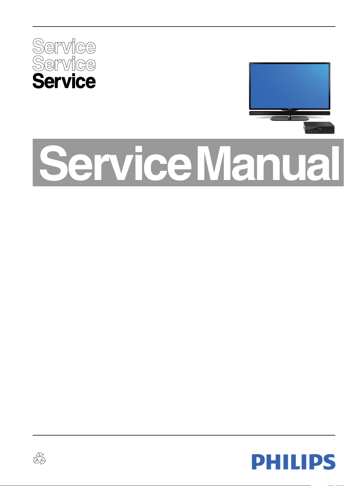
1.2 Connections
EN 3Q529.1E LC 1.
Note: The following connector colour abbreviations are used
(acc. to DIN/IEC 757): Bk= Black, Bu= Blue, Gn= Green,
Gy= Grey, Rd= Red, Wh= White, Ye= Yellow.
1.2.1 Connections
1 - Single cable connectors
Dedicated for Essence
2 - EXT1, EXT2: Video YPbPr - In, CVBS - In/Out, Audio - In/ Out
1 -Audio R 0.5 V
2 -Audio R 0.5 V
3 -Audio L 0.5 V
4 -Ground Audio Gnd H
5 -Ground Blue Gnd H
6 -Audio L 0.5 V
7 -Video Pb 0.7 V
8 -Function Select 0 - 2 V: INT
9 -Ground Gnd H
10 - n.c.
11 - Video Y 1 V
12 - n.c.
13 - Ground Gnd H
14 - Ground Gnd H
15 - Video Pr 0.7 V
20
21
Figure 1-2 SCART connector
E_06532_001.eps
/ 1 kohm k
RMS
/ 10 kohm j
RMS
/ 1 kohm k
RMS
/ 10 kohm j
RMS
/ 75 ohm j
PP
4.5 - 7 V: EXT 16:9
9.5 - 12 V: EXT 4:3 j
/ 75 ohm j
PP
/ 75 ohm j
PP
2
1
050404
Figure 1-1 Connection overview
16 - Status/FBL 0 - 0.4 V: INT
17 - Ground Video Gnd H
18 - Ground FBL Gnd H
19 - Video CVBS 1 V
20 - Video CVBS/Y 1 V
21 - Shield Gnd H
3a - EXT 3 VGA: Video RGB - In
1 -Video Red 0.7 V
2 -Video Green 0.7 V
3 -Video Blue 0.7 V
4-n.c.
5 -Ground Gnd H
6 -Ground Red Gnd H
7 -Ground Green Gnd H
8 -Ground Blue Gnd H
9-+5V
10 - Ground Sync Gnd H
11 - n.c.
12 - DDC_SDA DDC data j
13 - H-sync 0 - 5 V j
14 - V-sync 0 - 5 V j
15 - DDC_SCL DDC clock j
3b - Cinch: Audio - In
Rd - Audio R 0.5 V
Wh - Audio L 0.5 V
4 - Cinch: Audio - Out
Rd - Audio - R 0.5 V
Wh - Audio - L 0.5 V
1 - 3 V: EXT / 75 ohm j
/ 75 ohm k
PP
/ 75 ohm j
PP
Figure 1-3 VGA Connector
PP
PP
PP
DC
+5 V j
RMS
RMS
RMS
RMS
/ 75 Ω j
/ 75 Ω j
/ 75 Ω j
/ 10 kΩ jq
/ 10 kΩ jq
/ 10 kΩ kq
/ 10 kΩ kq
Page 4

EN 4 Q529.1E LC1.
19
1
18 2
E_06532_017.eps
250505
1 2 3 4
E_06532_022.eps
300904
112345678
E_06532_025.eps
210905
Technical Specifications, Connections, and Chassis Overview
5 - Cinch: Video YPbPr - In
Gn - Video Y 1 V
Bu - Video Pb 0.7 V
Rd - Video Pr 0.7 V
/ 75 Ω jq
PP
/ 75 Ω jq
PP
/ 75 Ω jq
PP
7, 11 - HDMI 1, 2, 3 Digital Video, Digital Audio - In
Figure 1-4 HDMI (type A) connector
1 -D2+ Data channel j
2-Shield Gnd H
3 -D2- Data channel j
4 -D1+ Data channel j
5-Shield Gnd H
6 -D1- Data channel j
7 -D0+ Data channel j
8-Shield Gnd H
9 -D0- Data channel j
10 - CLK+ Data channel j
11 - Shield Gnd H
12 - CLK- Data channel j
13 - Easylink Control channel jk
14 - n.c.
15 - DDC_SCL DDC clock j
16 - DDC_SDA DDC data jk
17 - Ground Gnd H
18 - +5V j
19 - HPD Hot Plug Detect j
20 - Ground Gnd H
17 - RJ45: Ethernet
Figure 1-6 Ethernet connector
1 -TD+ Transmit signal k
2 -TD- Transmit signal k
3 -RD+ Receive signal j
4-n.c.
5-n.c.
6 -RD- Receive signal j
7-n.c.
8-n.c.
18 - Common Interface
68p-See diagram B03H jk
8 - Cinch: S/PDIF - Out
Bk - Coaxial 0.4 - 0.6V
/ 75 Ω kq
PP
9 - Aerial - In
- - IEC-type (EU) Coax, 75 Ω D
10 - Service Connector (UART)
1 -Ground Gnd H
2 -UART_TX Transmit k
3 -UART_RX Receive j
12 - Cinch: Audio - In
Rd - Audio - R 0.5 V
Wh - Audio - L 0.5 V
/ 10 kΩ jq
RMS
/ 10 kΩ jq
RMS
13 - Headphone (Output)
Bk - Headphone 32 - 600 Ω / 10 mW ot
14 - Cinch: Audio - In
Rd - Audio - R 0.5 V
Wh - Audio - L 0.5 V
/ 10 kΩ jq
RMS
/ 10 kΩ jq
RMS
15 - Cinch: Video CVBS - In, Audio - In
Ye - Video CVBS 1 V
/ 75 Ω jq
PP
16 - USB2.0
1-+5V k
2 -Data (-) jk
3 -Data (+) jk
4 -Ground Gnd H
Figure 1-5 USB (type A)
Page 5
Technical Specifications, Connections, and Chassis Overview
I_18020_088.eps
110908
A
MAIN SUPPLY PANEL
G
I/O PANEL
LD
LV DS2DP
BOARD
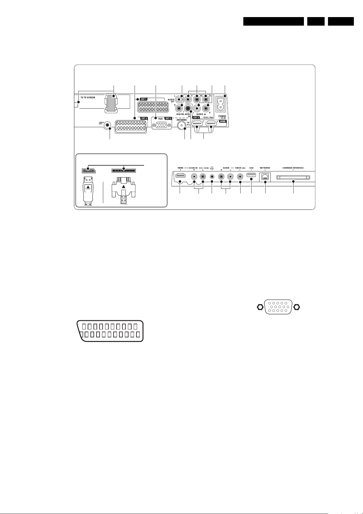
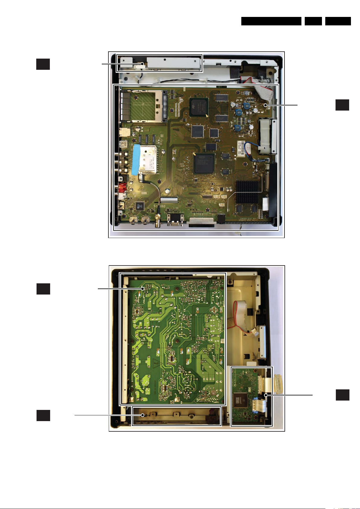
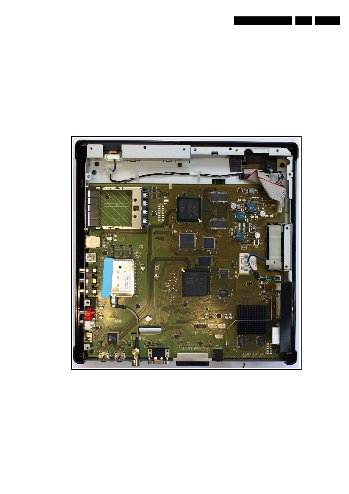
1.3 Chassis Overview
KEYBOARD CONTROL
E
PA NE L
EN 5Q529.1E LC 1.
Figure 1-7 PWB/CBA locations Hub -1-
SMALL SIGNAL
BOARD
I_18020_087.eps
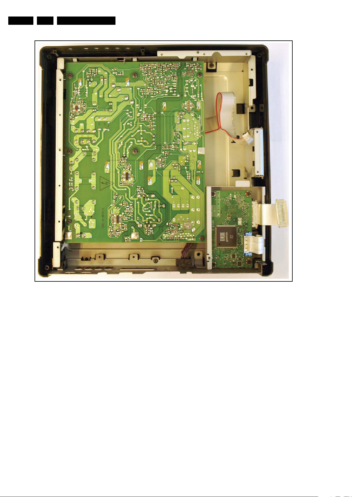
B
110908
Figure 1-8 PWB/CBA locations Hub -2-
Page 6
EN 6 Q529.1E LC1.
I_18020_089.eps
110908
J
IR & LED PANEL
M
MONITOR BOARD
Technical Specifications, Connections, and Chassis Overview
Figure 1-9 PWB/CBA locations Monitor
Page 7

Safety Instructions, Warnings, and Notes
2. S afety Instructions, Warnings, and Notes
EN 7Q529.1E LC 2.
Index of this chapter:
2.1 Safety Instructions
2.2 Warnings
2.3 Notes
2.1 Safety Instructions
Safety regulations require the following during a repair:
• Connect the set to the Mains/AC Power via an isolation
transformer (> 800 VA).
• Replace safety components, indicated by the symbol h,
only by components identical to the original ones. Any
other component substitution (other than original type) may
increase risk of fire or electrical shock hazard.
Safety regulations require that after a repair, the set must be
returned in its original condition. Pay in particular attention to
the following points:
• Route the wire trees correctly and fix them with the
mounted cable clamps.
• Check the insulation of the Mains/AC Power lead for
external damage.
• Check the strain relief of the Mains/AC Power cord for
proper function.
• Check the electrical DC resistance between the Mains/AC
Power plug and the secondary side (only for sets that have
a Mains/AC Power isolated power supply):
1. Unplug the Mains/AC Power cord and connect a wire
between the two pins of the Mains/AC Power plug.
2. Set the Mains/AC Power switch to the “on” position
(keep the Mains/AC Power cord unplugged!).
3. Measure the resistance value between the pins of the
Mains/AC Power plug and the metal shielding of the
tuner or the aerial connection on the set. The reading
should be between 4.5 MΩ and 12 MΩ.
4. Switch “off” the set, and remove the wire between the
two pins of the Mains/AC Power plug.
• Check the cabinet for defects, to prevent touching of any
inner parts by the customer.
2.2 Warnings
• All ICs and many other semiconductors are susceptible to
electrostatic discharges (ESD w). Careless handling
during repair can reduce life drastically. Make sure that,
during repair, you are connected with the same potential as
the mass of the set by a wristband with resistance. Keep
components and tools also at this same potential.
• Be careful during measurements in the high voltage
section.
• Never replace modules or other components while the unit
is switched “on”.
• When you align the set, use plastic rather than metal tools.
This will prevent any short circuits and the danger of a
circuit becoming unstable.
2.3 Notes
2.3.1 General
• Measure the voltages and waveforms with regard to the
chassis (= tuner) ground (H), or hot ground (I), depending
on the tested area of circuitry. The voltages and waveforms
shown in the diagrams are indicative. Measure them in the
Service Default Mode (see chapter 5) with a colour bar
signal and stereo sound (L: 3 kHz, R: 1 kHz unless stated
otherwise) and picture carrier at 475.25 MHz for PAL, or
61.25 MHz for NTSC (channel 3).
• Where necessary, measure the waveforms and voltages
with (D) and without (E) aerial signal. Measure the
voltages in the power supply section both in normal
operation (G) and in stand-by (F). These values are
indicated by means of the appropriate symbols.
• Manufactured under license from Dolby Laboratories.
“Dolby”, “Pro Logic” and the “double-D symbol”, are
trademarks of Dolby Laboratories.
2.3.2 Schematic Notes
• All resistor values are in ohms, and the value multiplier is
often used to indicate the decimal point location (e.g. 2K2
indicates 2.2 kΩ).
• Resistor values with no multiplier may be indicated with
either an “E” or an “R” (e.g. 220E or 220R indicates 220 Ω).
• All capacitor values are given in micro-farads (μ=× 10
nano-farads (n =× 10
• Capacitor values may also use the value multiplier as the
decimal point indication (e.g. 2p2 indicates 2.2 pF).
• An “asterisk” (*) indicates component usage varies. Refer
to the diversity tables for the correct values.
• The correct component values are listed in the Spare Parts
List. Therefore, always check this list when there is any
doubt.
2.3.3 BGA (Ball Grid Array) ICs
Introduction
For more information on how to handle BGA devices, visit this
URL: www.atyourservice.ce.philips.com (needs subscription,
not available for all regions). After login, select “Magazine”,
then go to “Repair downloads”. Here you will find Information
on how to deal with BGA-ICs.
BGA Temperature Profiles
For BGA-ICs, you must use the correct temperature-profile,
which is coupled to the 12NC. For an overview of these profiles,
visit the website www.atyourservice.ce.philips.com (needs
subscription, but is not available for all regions)
You will find this and more technical information within the
“Magazine”, chapter “Repair downloads”.
For additional questions please contact your local repair help
desk.
2.3.4 Lead-free Soldering
Due to lead-free technology some rules have to be respected
by the workshop during a repair:
• Use only lead-free soldering tin Philips SAC305 with order
code 0622 149 00106. If lead-free solder paste is required,
please contact the manufacturer of your soldering
equipment. In general, use of solder paste within
workshops should be avoided because paste is not easy to
store and to handle.
• Use only adequate solder tools applicable for lead-free
soldering tin. The solder tool must be able:
– To reach a solder-tip temperature of at least 400°C.
– To stabilize the adjusted temperature at the solder-tip.
– To exchange solder-tips for different applications.
• Adjust your solder tool so that a temperature of around
360°C - 380°C is reached and stabilized at the solder joint.
Heating time of the solder-joint should not exceed ~ 4 sec.
Avoid temperatures above 400°C, otherwise wear-out of
tips will increase drastically and flux-fluid will be destroyed.
To avoid wear-out of tips, switch “off” unused equipment or
reduce heat.
• Mix of lead-free soldering tin/parts with leaded soldering
tin/parts is possible but PHILIPS recommends strongly to
-9
), or pico-farads (p =× 10
-12
-6
),
).
Page 8

EN 8 Q529.1E LC3.
E_06532_024.eps
260308
MODEL :
PROD.NO:
~
S
32PF9968/10
MADE IN BELGIUM
220-240V 50/60Hz
128W
AG 1A0617 000001
VHF+S+H+UHF
BJ3.0E LA
Directions for Use
avoid mixed regimes. If this cannot be avoided, carefully
clear the solder-joint from old tin and re-solder with new tin.
2.3.5 Alternative BOM identification
It should be noted that on the European Service website,
“Alternative BOM” is referred to as “Design variant”.
The third digit in the serial number (example:
AG2B0335000001) indicates the number of the alternative
B.O.M. (Bill Of Materials) that has been used for producing the
specific TV set. In general, it is possible that the same TV
model on the market is produced with e.g. two different types
of displays, coming from two different suppliers. This will then
result in sets which have the same CTN (Commercial Type
Number; e.g. 28PW9515/12) but which have a different B.O.M.
number.
By looking at the third digit of the serial number, one can
identify which B.O.M. is used for the TV set he is working with.
If the third digit of the serial number contains the number “1”
(example: AG1B033500001), then the TV set has been
manufactured according to B.O.M. number 1. If the third digit is
a “2” (example: AG2B0335000001), then the set has been
produced according to B.O.M. no. 2. This is important for
ordering the correct spare parts!
For the third digit, the numbers 1...9 and the characters A...Z
can be used, so in total: 9 plus 26= 35 different B.O.M.s can be
indicated by the third digit of the serial number.
Identification: The bottom line of a type plate gives a 14-digit
serial number. Digits 1 and 2 refer to the production center (e.g.
AG is Bruges), digit 3 refers to the B.O.M. code, digit 4 refers
to the Service version change code, digits 5 and 6 refer to the
production year, and digits 7 and 8 refer to production week (in
example below it is 2006 week 17). The 6 last digits contain the
serial number.
Figure 2-1 Serial number (example)
2.3.6 Board Level Repair (BLR) or Component Level Repair (CLR)
If a board is defective, consult your repair procedure to decide
if the board has to be exchanged or if it should be repaired on
component level.
If your repair procedure says the board should be exchanged
completely, do not solder on the defective board. Otherwise, it
cannot be returned to the O.E.M. supplier for back charging!
2.3.7 Practical Service Precautions
• It makes sense to avoid exposure to electrical shock.
While some sources are expected to have a possible
dangerous impact, others of quite high potential are of
limited current and are sometimes held in less regard.
• Always respect voltages. While some may not be
dangerous in themselves, they can cause unexpected
reactions that are best avoided. Before reaching into a
powered TV set, it is best to test the high voltage insulation.
It is easy to do, and is a good service precaution.
3. Directions for Use
Directions for use can be downloaded from the following
websites:
http://www.philips.com/support
http://www.p4c.philips.com
Page 9
4. Mechanical Instructions
I_18020_090.eps
110908
Index of this chapter:
4.1 Cable Dressing
4.2 Service Positions
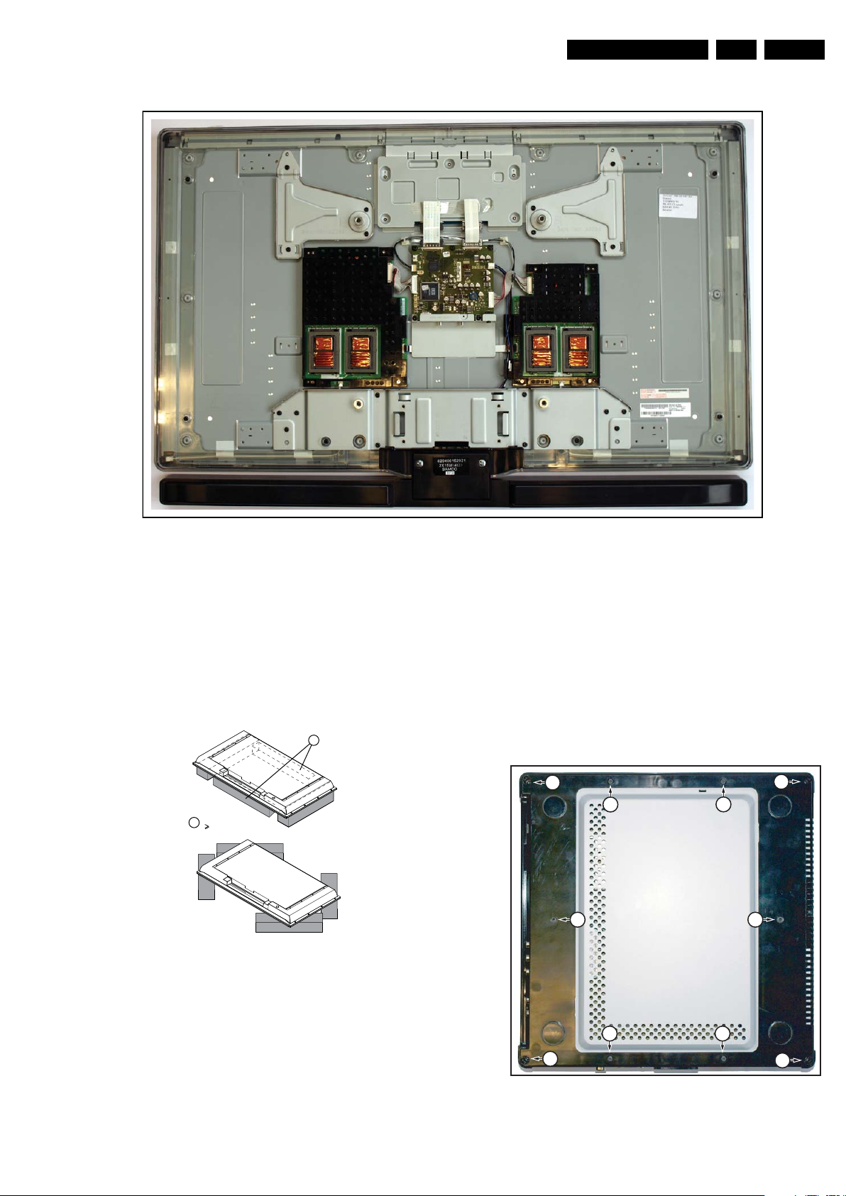
4.3 Assy/Panel Removal Hub
4.4 Assy/Panel Removal Monitor
4.5 Set Re-assembly.
Notes:
• Figures below can deviate slightly from the actual situation,
due to the different set executions.
4.1 Cable Dressing
Mechanical Instructions
EN 9Q529.1E LC 4.
Figure 4-1 Cable dressing hub; bottom view
Page 10
EN 10 Q529.1E LC4.
I_18020_091.eps
110908
Mechanical Instructions
Figure 4-2 Cable dressing hub; bottom view (SSB removed)
Page 11
Mechanical Instructions
I_18020_092.eps
110908
E_06532_018.eps
171106
1
Required for sets
42"
1
I_18020_143.eps
081008
11
1
1
1
1
1
1
1
1
EN 11Q529.1E LC 4.
4.2 Service Positions
For easy servicing of the monitor of the set, there are a few
possibilities created:
• The buffers from the packaging.
• Foam bars (created for Service).
4.2.1 Foam Bars
Figure 4-3 Cable dressing monitor
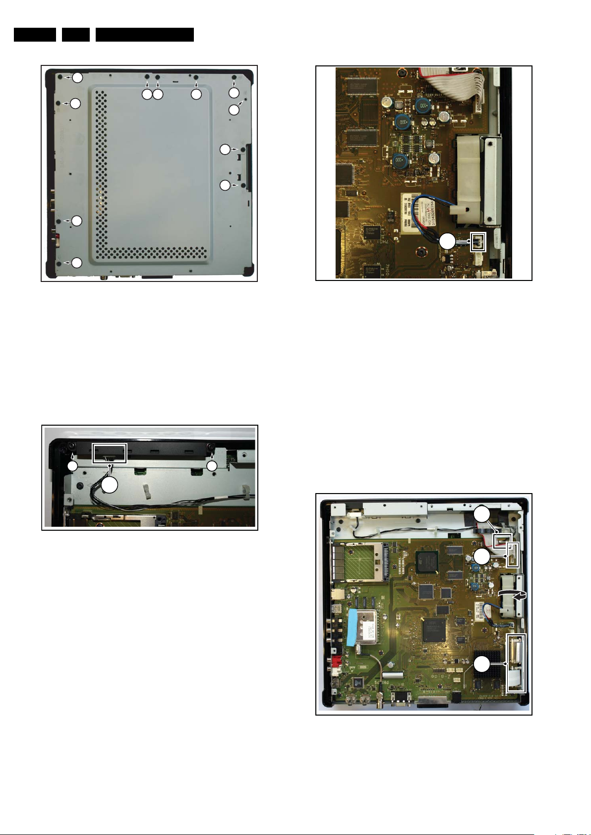
4.3 Assy/Panel Removal Hub
4.3.1 Bottom Cover and -Shield
Warning: Disconnect the mains power cord before removing
the rear cover.
Refer to next figures for details.
1. Place the hub upside-down and remove the bottom cover
by removing the screws [1].
2. Remove the bottom shield by removing the screws [2]
indicated with an arrow.
Figure 4-4 Foam bars
The foam bars (order code 3122 785 90580 for two pieces) can
be used for all types and sizes of Flat TVs. See figure “Foam
bars” for details. Sets with a display of 42" and larger, require
four foam bars [1]. Ensure that the foam bars are always
supporting the cabinet and never only the display.
Caution: Failure to follow these guidelines can seriously
damage the display!
By laying the TV face down on the (ESD protective) foam bars,
a stable situation is created to perform measurements and
alignments. By placing a mirror under the TV, the screen can
be monitored.
Figure 4-5 Bottom Cover and -Shield -1-
Page 12
EN 12 Q529.1E LC4.
I_18020_093.eps
081008
2
2
2
2
2
2
2
2 2 2
2
I_18020_094.eps
190908
2 2
1
I_18020_095.eps
190908
1
I_18020_096.eps
110908
2
3
(2x)
1
Mechanical Instructions
Figure 4-6 Bottom Cover and -Shield -2-
4.3.2 Key Board
Refer to next figure for details.
1. Unplug the key board connector [1] from the IR & LED
board.
2. Remove the screws [2].
3. Lift the unit and take it out of the set.
When defective, replace the whole unit.
Figure 4-7 Keyboard Control Panel
4.3.3 Fan
Figure 4-8 Fan
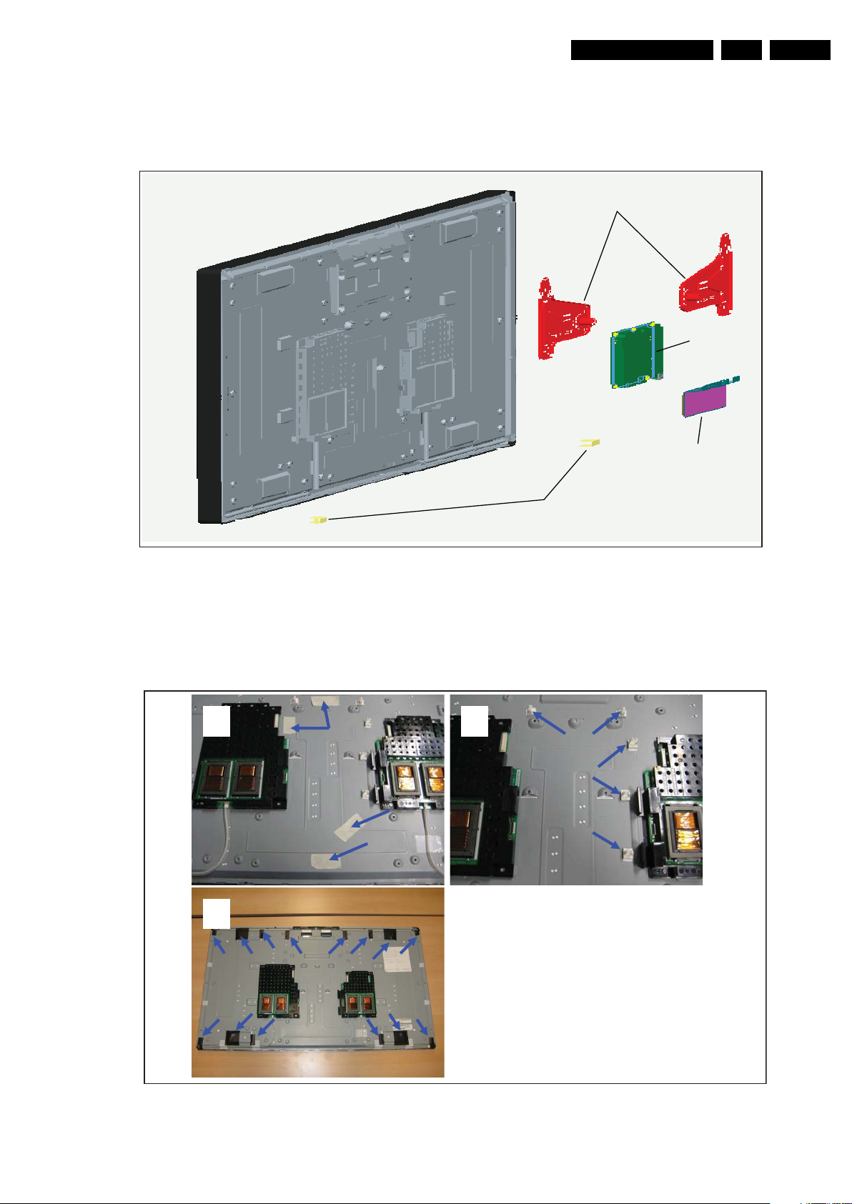
4.3.4 Small Signal Board (SSB)
Refer to next figures or details.
1. Remove fan.
2. Unplug keyboard cable [1] on SSB.
3. Unplug flat cable [2] on SSB.
4. Unplug two LVDS connectors [3] on SSB. These are very
fragile connectors!
5. Lift the flatcable gently with a screwdriver [4] that leads to
the underlaying I/O Panel.
6. Remove three screws near side I/O Panel.
7. Remove four screws near back I/O Panel (including the two
screws of the VGA connector).
8. Remove all remaining screws that secure the SSB.
9. Slide the SSB sidewards out of the hub.
Refer to next figure for details.
1. Unplug connector [1].
2. Lift the fan from the set. During replacement, ensure you
replace it at its original position.
When defective, replace the unit.
Figure 4-9 Small Signal Board -1-
Page 13
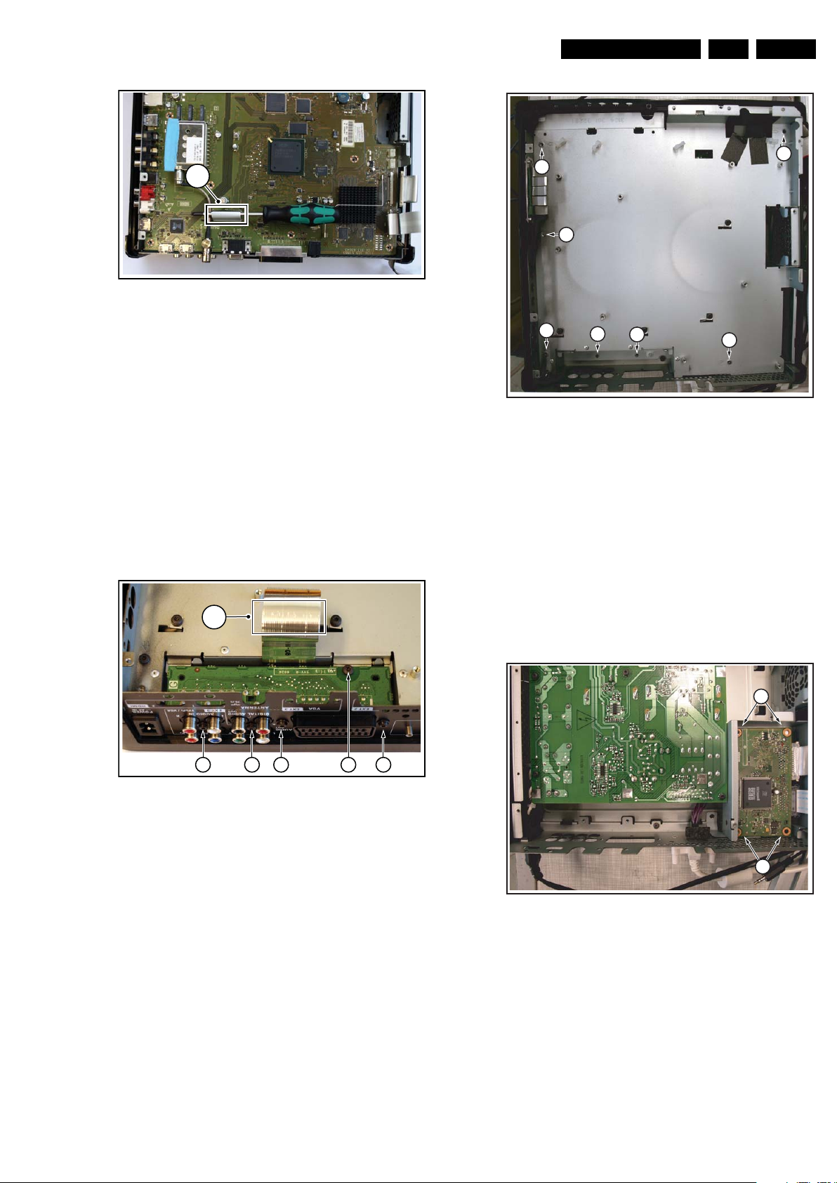
Figure 4-10 Small Signal Board -2-
I_18020_097.eps
110908
4
I_18020_119.eps
151008
1 1 2 23
4
I_18020_144.eps
151008
5
5
5
5
5
5
5
I_18020_098.eps
151008
1
1
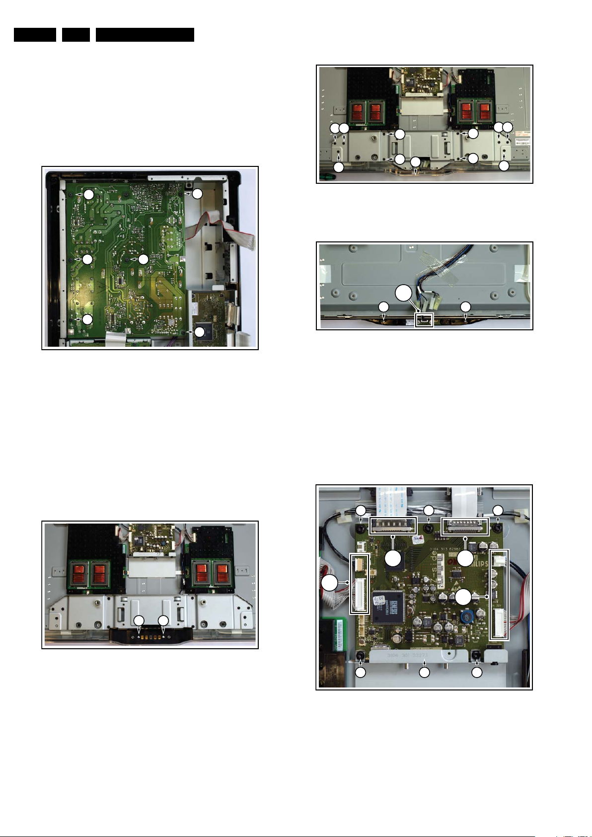
4.3.5 Subframe underneath SSB
Refer to next figures for details.
1. Remove keyboard, fan and SSB.
2. Remove two screws [1] on Additional I/O Panel (near cinch
plugs).
3. Remove two screw [2] on Additional I/O Panel (near
SCART plug).
4. Remove screw [3].
5. Unclamp flat cable coming from Power Supply Unit [4].
6. Take the board out.
7. Remove screws on the subframe indicated with an arrow
[5].
8. Lift the subframe on the right side, then lift the subframe
forwards, then take the subframe out of the hub.
Mechanical Instructions
4.3.6 Additional I/O Panel
Refer to section “Subframe underneath SSB”.
When defective, replace the whole unit.
4.3.7 Display Port Panel Hub
EN 13Q529.1E LC 4.
Figure 4-12 Subframe -2-
Refer to next figure for details.
1. Remove screws [1].
2. Unplug the other connectors.
3. Remove all fixation screws.
4. Take the board out.
Figure 4-11 Subframe -1-
Figure 4-13 Display Port Panel Hub
Page 14
EN 14 Q529.1E LC4.
I_18020_100.eps
110908
1
11
1
1
1
I_18020_101.eps
110908
1 1
I_18020_102.eps
110908
1
2
1
1
111
1
1
1
1
I_18020_103.eps
110908
4 4
3
I_18020_104.eps
110908
2 2
5 55
1
(2x)
1
(2x)
3 34
4.3.8 Power Supply Unit
Refer to next figure for details.
1. Remove the fixation screws [1].
2. Lift the board.
3. Unplug the connector to the mains inlet.
4. Unplug the connector from the supply connector to the
screen.
5. Take the supply out.
When defective, replace the whole unit.
Mechanical Instructions
Figure 4-16 IR & LED Panel -1-
Figure 4-14 Power Supply Unit
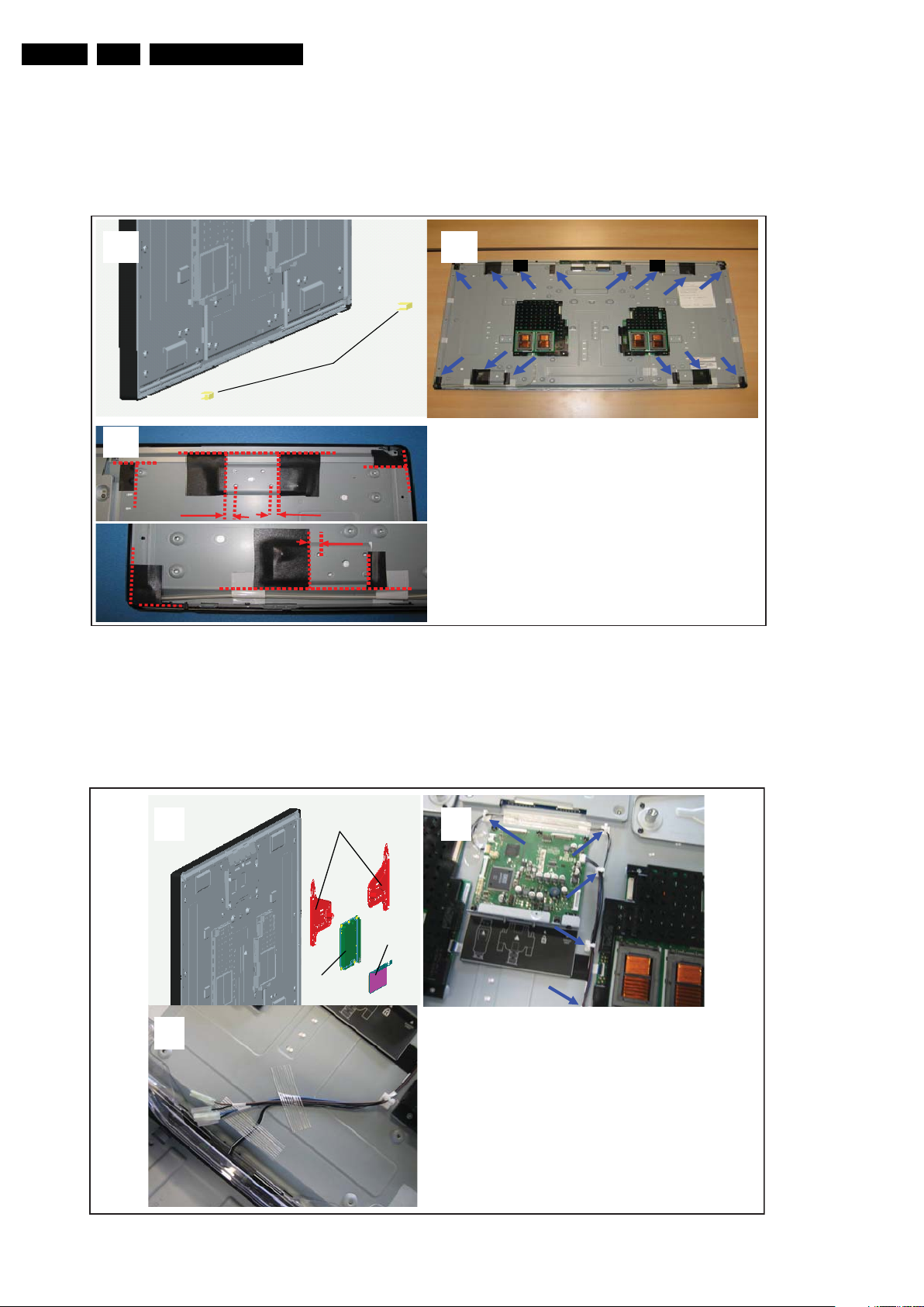
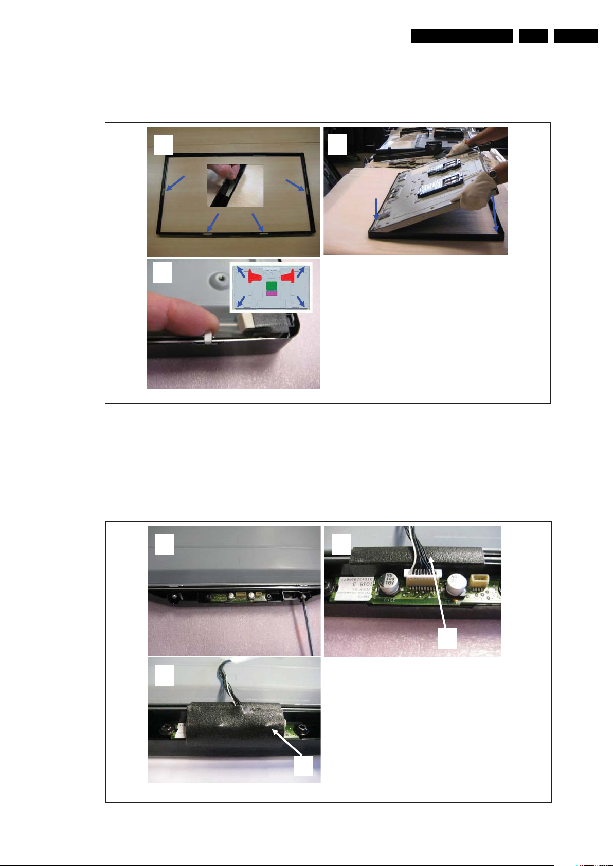
4.4 Assy/Panel Removal Monitor
4.4.1 Sound Interface
Refer to next figure for details.
1. Remove stand (four screws).
2. Lift set from stand.
3. Remove soundbar.
4. Remove sound interface by removing the screws [1].
When defective, replace the whole module.
Figure 4-17 IR & LED Panel -2-
4.4.3 Display Port Panel
Refer to next figure for details.
1. Unplug connectors [1].
2. Unplug LVDS connectors [2]. Be careful, as these are very
fragile connectors.
3. Remove screws [3] and subframe [4].
4. Remove screws [5].
When defective, replace the whole unit.
4.4.2 IR & LED Board
Refer to next figures for details.
1. Remove lower part of VESA stand [1].
2. Remove flare [2] (six screws).
3. Unplug connector [3].
4. Remove screws [4].
When defective, replace the whole unit.
Figure 4-15 Sound Interface
Figure 4-18 Display Port Panel Monitor
Page 15
Mechanical Instructions
Stand
Back Cover
Soundbar
Stand
Bracket
Flare
Sound Interface
Leading Edge
I_18020_105.eps
151008
EN 15Q529.1E LC 4.
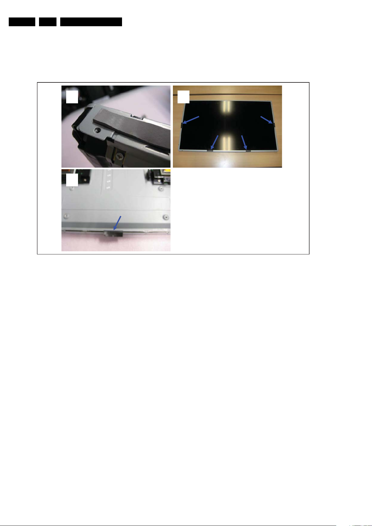
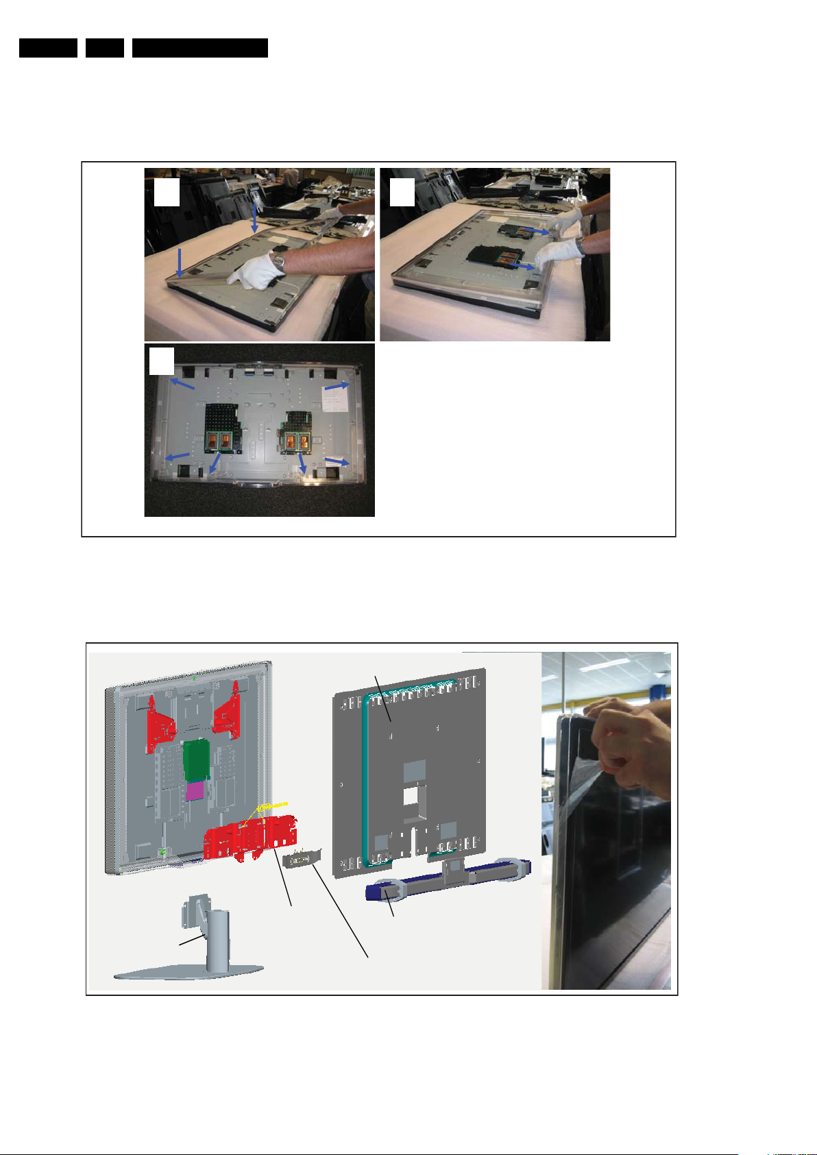
4.4.4 LCD Panel
SPECIAL NOTICE
The dis-assembly, re-assembly and/or exchange of the
LCD Panel is an elaborate process. Reason for this is the
mounting method of the Panel in the cabinet. Due to physical
restraints, no screws could be used, but instead adhesive
foams and -tapes are used.
Use gloves where indicated to avoid personal injury and
pollution of the LCD Panel (dust and/or fingerprints).
Exactly follow the instructions to avoid warranty issues,
especially when a defective LCD Panel has to be returned to
the supplier.
Step A. to F. describe the removal of the LCD Panel of the
cabinet.
Step K. to N. describe the mounting of the LCD Panel back into
the cabinet.
Step G. to J. describe which additional actions have to be taken
in the event the original LCD Panel has to be replaced.
Additional Spare Parts are needed when remounting the (new)
LCD Panel in the cabinet. These spare parts can be ordered as
one Service Kit using ordering code 3122 785 91150. The kit
contains the following items:
• 5 x Foam L × W × T = 20 × 43 × 0.5 mm.
• 6 x Foam L × W × T = 70 × 50 × 0.5 mm.
• 4 x Foam L × W × T = 30 × 43 × 0.5 mm.
• 1 x Foam L × W × T = 55 × 20 × 0.8 mm.
• 5 x Cable clamp (wire saddle) 11.2 mm.
LCD Panel Removal
A. Refer to next figure for details.
1. Remove stand.
2. Remove soundbar.
3. Remove backcover.
4. Remove sound interface.
5. Remove flare.
6. Remove stand bracket.
7. Remove leading edge.
Figure 4-19 LCD Panel -1-
Page 16
EN 16 Q529.1E LC4.
I_18020_106.eps
110908
1
3
2
I_18020_107.eps
180908
B. Bend metal lips in each corner of Front open.
Mechanical Instructions
Figure 4-20 LCD Panel -2-
C. Remove thermal foams (3x) between LCD-panel and upper
wall of metal Front.
1. Pull the upper bend open.
2. Move out the thermal foam with e.g. a screwdriver.
3. Pull out the thermal foam.
Figure 4-21 LCD Panel -3-
Page 17

Mechanical Instructions
1
3
2
I_18020_108.eps
110908
1
3
2
I_18020_109.eps
180908
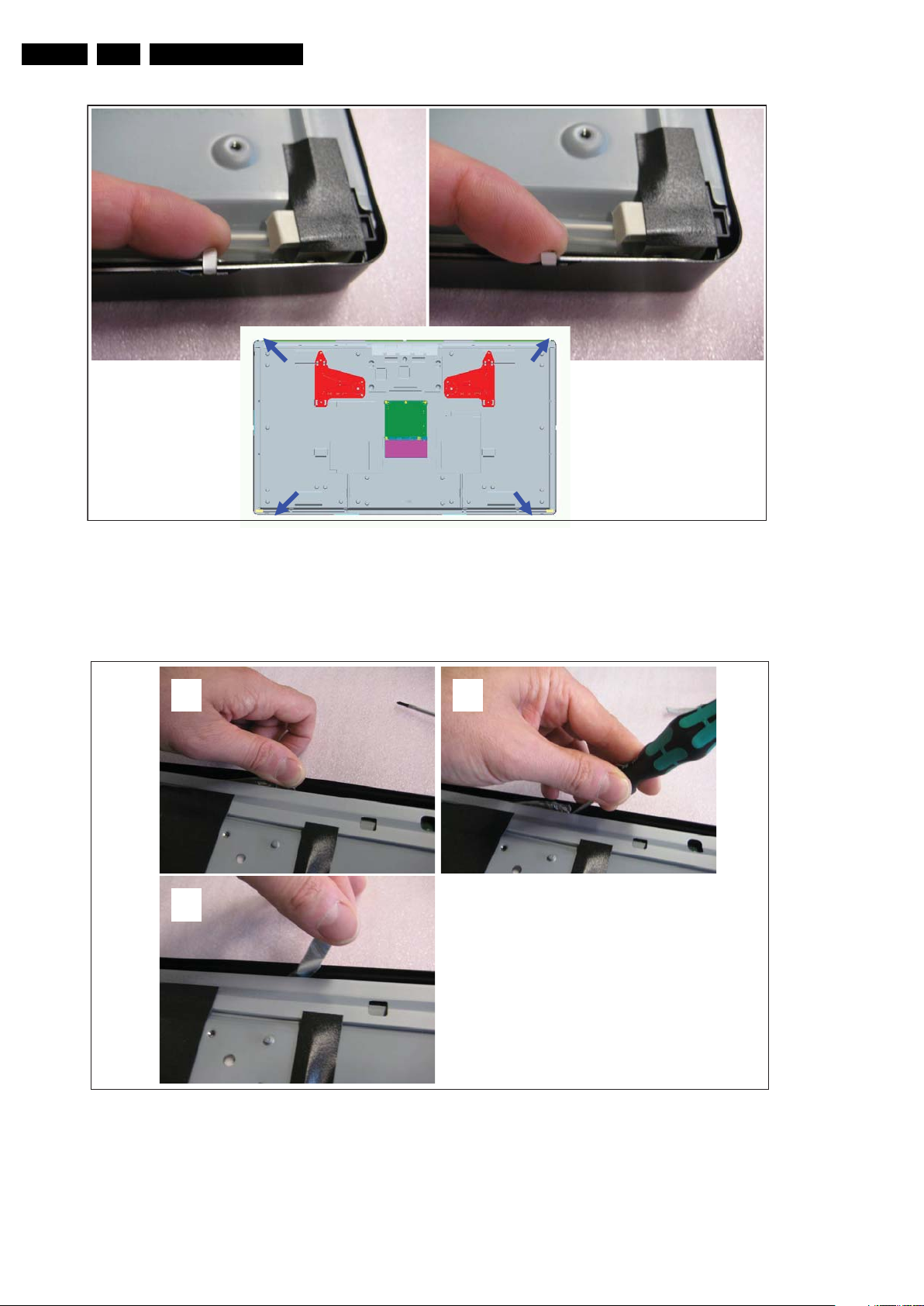
D. Release two side walls of metal Front (use gloves).
1. Place thumb against each upper corner of the metal Front.
2. Place fingers against LCD Panel.
3. Push out LCD Panel in each corner until tape in middle of
side wall releases.
EN 17Q529.1E LC 4.
Figure 4-22 LCD Panel -4-
E. Release bottom wall of metal Front (use gloves).
1. Place hands in top/middle of metal Front and LCD Panel.
2. Pull metal Front and LCD Panel further apart until 2 tapes
in bottom wall release.
3. Take out LCD Panel.
Figure 4-23 LCD Panel -5-
Page 18
EN 18 Q529.1E LC4.
1
3
2
I_18020_110.eps
110908
F. Removing tapes/foams from LCD Panel (use “Label Off 50”;
“Intronics L50/200”).
1. Remove remains of thermal foam on top of LCD Panel.
2. Remove remains of double-sided tapes (4x) on front of
LCD Panel.
3. Remove protective foam on bottom of LCD Panel.
Mechanical Instructions
For re-assembly instructions, proceed with step K.
Figure 4-24 LCD Panel -6-
Page 19
Mechanical Instructions
Vesa Brackets
Connector
Plate
PCB
Isolator
Plates
I_18020_111.eps
151008
1
3
2
I_18020_112.eps
120908
LCD Panel Replacement
Instructions G to J apply if you have to replace the LCD
Panel.
G. Remove VESA brackets, PCB connector plate, wiring, and
isolator plates.
EN 19Q529.1E LC 4.
Figure 4-25 LCD Panel -7-
H. Remove all remaining tapes/foams/cable clamps.
1. Remove remaining tapes for wiring.
2. Remove cable clamps (five times).
3. Remove all backlight blocking foams.
4. Remove all glue remains with “Label Off 50”.
Figure 4-26 LCD Panel -8-
Page 20
EN 20 Q529.1E LC4.
1 2
Isolator
Plates
3
10±5 10±5
3
10±5
AB
C
A
B
C
B
A
B
BBBC
C
B
A
A
B
C
C
A
I_18020_113.eps
171008
1
3
2
Vesa Brackets
Connector
Plate
PCB
I_18020_114.eps
180908
I. Prepare new LCD Panel.
1. Take new LCD Panel and place two isolator plates.
2. Glue new foams on LCD Panel with the following
specifications:
- four times foam L × W × T = 20 × 43 × 0.5 mm [A].
- six times foam L × W × T = 70 × 50 × 0.5 mm [B].
- four times foam L × W × T = 30 × 43 × 0.5 mm [C].
3. Figure [3] show the upper- and lower foams.
Mechanical Instructions
Figure 4-27 LCD Panel -9-
J. Assemble VESA brackets, PCB, connector plate, and wiring.
1. Assemble VESA brackets, PCB and connector plate.
2. Assemble cable clamps:
- five times cable clamp 11.2 mm.
3. Assemble wiring.
Figure 4-28 LCD Panel -10-
Page 21
Mechanical Instructions
1
3
2
1
2
3
2
I_18020_115.eps
171008
1
3
2
A
B
I_18020_116.eps
180908
K. Assemble metal Front and LCD Panel (use gloves).
1. Take a new metal Front and remove liners of double-sided
tapes (four times).
2. Insert LCD Panel as shown in picture: first top side, then
cantilever down.
3. Bend down metal lips in each corner (4 times).
EN 21Q529.1E LC 4.
Figure 4-29 LCD Panel -11-
L. Assemble Leading Edge.
1. Assemble Leading Edge on Front.
2. Glue protective foam across edge of metal Front and LCD
Panel with the following specifications:
1 time foam L × W × T = 55 × 20 × 0.8 mm [A].
3. Glue light-blocking foam upon LED-PCB with the following
specifications:
1 time foam L × W × T = 20 × 43 × 0.5 mm [B].
Figure 4-30 LCD Panel -12-
Page 22
EN 22 Q529.1E LC4.
Stand
Back Cover
Soundbar
Stand
Bracket
Sound Interface
I_18020_118.eps
180908
M. Assemble Flare.
1. Place flare upon LCD Panel as shown in picture: first on top
side.
2. Cantilever flare down while pulling it slightly open (to avoid
scratches from metal Front).
3. Fix flare on Panel (six screws).
Mechanical Instructions
1
1
1
3
3
Figure 4-31 LCD Panel -13-
N. Assemble Stand Bracket, Sound Interface, Back Cover,
Soundbar and Stand.
1. Remove protective foils on both sides of Flare.
2
I_18020_117.eps
171008
Figure 4-32 LCD Panel -14-
Page 23

4.5 Set Re-assembly
To re-assemble the whole set, execute all processes in reverse
order, except for the Monitor. To re-assembly the Monitor,
follow the instructions in the applicable section of this Manual.
Notes:
• While re-assembling, make sure that all cables are placed
and connected in their original position. See figure “Cable
dressing”.
• Pay special attention not to damage the EMC foams on the
SSB shields. Ensure that EMC foams are mounted
correctly.
Mechanical Instructions
EN 23Q529.1E LC 4.
Page 24
EN 24 Q529.1E LC5.
I_18020_146.eps
190908
1
SDM1SDM
1
SDM2SPI-P
Service Modes, Error Codes, and Fault Finding
5. S ervice Modes, Error Codes, and Fault Finding
Index of this chapter:
5.1 Test Points
5.2 Service Modes
5.3 Stepwise Start-up
5.4 Service Tools
5.5 Error Codes
5.6 The Blinking LED Procedure
5.7 Protections
5.8 Fault Finding and Repair Tips
5.9 Software Upgrading
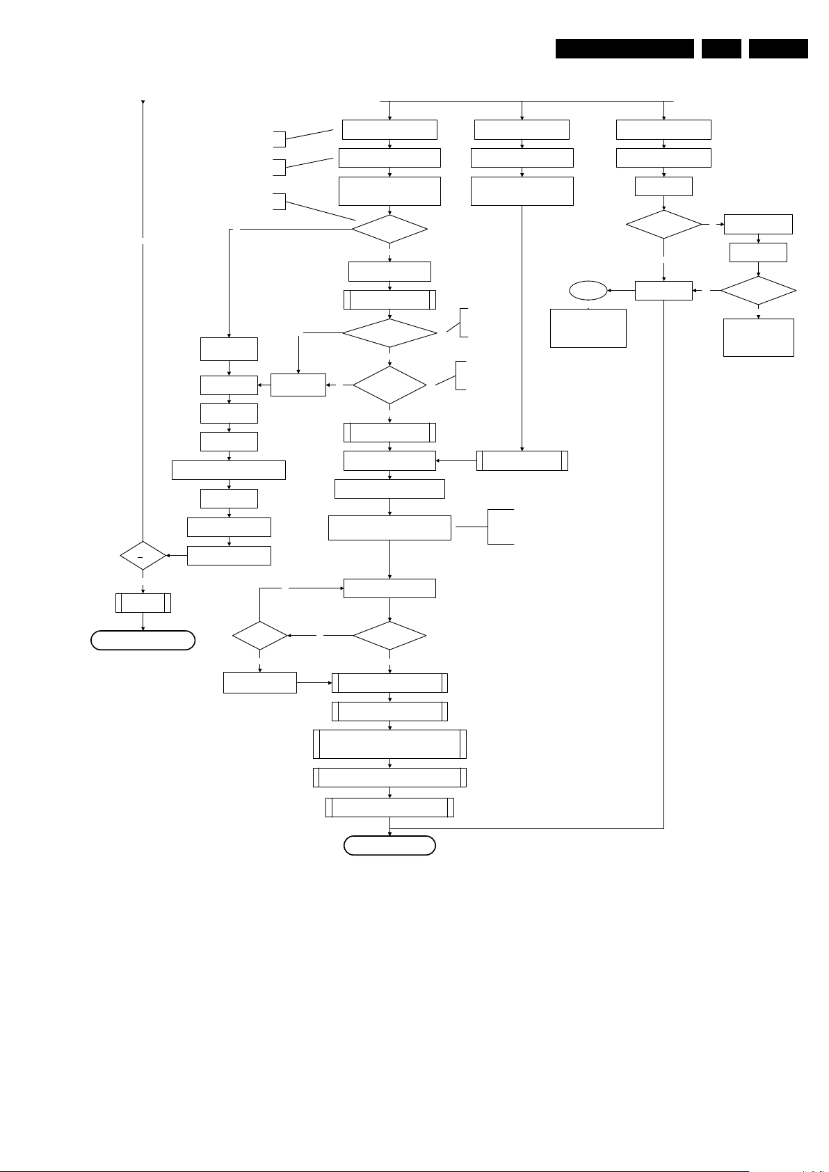
5.1 Test Points
As most signals are digital, it will be difficult to measure
waveforms with a standard oscilloscope. However, several key
ICs are capable of generating test patterns, which can be
controlled via ComPair. In this way it is possible to determine
which part is defective.
Perform measurements under the following conditions:
• Service Default Mode.
• Video: Colour bar signal.
• Audio: 3 kHz left, 1 kHz right.
5.2 Service Modes
Service Default mode (SDM) and Service Alignment Mode
(SAM) offers several features for the service technician, while
the Customer Service Mode (CSM) is used for communication
between the call centre and the customer.
This chassis also offers the option of using ComPair, a
hardware interface between a computer and the TV chassis. It
offers the abilities of structured troubleshooting, error code
reading, and software version read-out for all chassis.
(see also section “5.4.1 ComPair”).
– Skip/blank of non-favourite pre-sets.
How to Activate SDM
For this chassis there are two kinds of SDM: an analog SDM
and a digital SDM. Tuning will happen according table “SDM
Default Settings”.
• Analog SDM: use the standard RC-transmitter and key in
the code “062596”, directly followed by the “MENU” button.
Note: It is possible that, together with the SDM, the main
menu will appear. To switch it “off”, push the “MENU”
button again.
• Digital SDM: use the standard RC-transmitter and key in
the code “062593”, directly followed by the “MENU” button.
Note: It is possible that, together with the SDM, the main
menu will appear. To switch it “off”, push the “MENU”
button again.
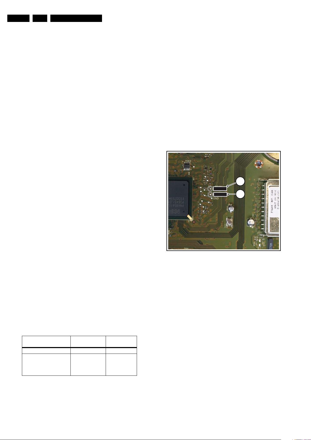
• Analog SDM can also be activated by connecting for a
moment the solder pad (see figure “Service mode pads”)
on the SSB with the indication “SDM” [1], to GND.
5.2.1 Service Default Mode (SDM)
Purpose
• To create a pre-defined setting, to get the same
measurement results as given in this manual.
• To override SW protections detected by stand-by
processor and make the TV start up to the step just before
protection (a sort of automatic stepwise start up). See
section “5.3 Stepwise Start-up”.
• To start the blinking LED procedure where only layer 2
errors are displayed. (see also section “5.5 Error Codes”)
Specifications
Table 5-1 SDM default settings
Region Freq. (MHz)
Europe, AP(PAL/Multi) 475.25 PAL B/G
Europe, AP DVB-T 546.00 PID
• All picture settings at 50% (brightness, colour, contrast).
• All sound settings at 50%, except volume at 25%.
• All service-unfriendly modes (if present) are disabled, like:
– (Sleep) timer.
– Child/parental lock.
– Picture mute (blue mute or black mute).
– Automatic volume levelling (AVL).
Video: 0B 06 PID
PCR: 0B 06 PID
Audio: 0B 07
Default
system
DVB-T
Figure 5-1 Service mode pads
After activating this mode, “SDM” will appear in the upper right
corner of the screen (when a picture is available).
How to Navigate
When the “MENU” button is pressed on the RC transmitter, the
set will toggle between the SDM and the normal user menu
(with the SDM mode still active in the background).
How to Exit SDM
Use one of the following methods:
• Switch the set to STAND-BY via the RC-transmitter.
• Via a standard customer RC-transmitter: key in “00”sequence.
5.2.2 Service Alignment Mode (SAM)
Purpose
• To perform (software) alignments.
• To change option settings.
• To easily identify the used software version.
• To view operation hours.
• To display (or clear) the error code buffer.
How to Activate SAM
Via a standard RC transmitter: key in the code “062596”
directly followed by the “INFO” button. After activating SAM
Page 25

PHILIPS
MODEL:
32PF9968/10
PROD.SERIAL NO:
AG 1A0620 000001
040
39mm
27mm
(CTN Sticker)
Display Option
Code
E_06532_038.eps
240108
Service Modes, Error Codes, and Fault Finding
EN 25Q529.1E LC 5.
with this method a service warning will appear on the screen,
continue by pressing the red button on the RC.
Contents of SAM:
• Hardware Info.
– A. SW Version. Displays the software version of the
main software (example: Q591E-1.2.3.4 =
AAAAB_X.Y.W.Z).
• AAAA= the chassis name.
• B= the region: A= AP, E= EU, L= Latam, U = US.
For AP sets it is possible that the Europe software
version is used.
• X.Y.W.Z= the software version, where X is the
main version number (different numbers are not
compatible with one another) and Y.W.Z is the sub
version number (a higher number is always
compatible with a lower number).
– B. SBY PROC Version. Displays the software version
of the stand-by processor.
– C. Production Code. Displays the production code of
the TV, this is the serial number as printed on the back
of the TV set. Note that if an NVM is replaced or is
initialized after corruption, this production code has to
be re-written to NVM. ComPair will foresee in a
possibility to do this.
• Operation Hours. Displays the accumulated total of
operation hours (not the stand-by hours). Every time the
TV is switched “on/off”, 0.5 hours is added to this number.
• Errors (followed by maximum 10 errors). The most recent
error is displayed at the upper left (for an error explanation
see section “5.5 Error Codes”).
• Reset Error Buffer. When “cursor right” (or the “OK
button) is pressed followed by another “OK” button touch,
the error buffer is reset.
• Alignments. This will activate the “ALIGNMENTS” submenu.
• Dealer Options. Extra features for the dealers.
• Options. Extra features for Service. For more info
regarding option codes, see chapter 8 “Alignments”.
Note that if the option code numbers are changed, these
have to be confirmed with pressing the “OK” button before
the options are stored. Otherwise changes will be lost.
• Initialize NVM. The moment the processor recognizes a
corrupted NVM, the “initialize NVM” line will be highlighted.
Now, two things can be done (dependent of the service
instructions at that moment):
– Save the content of the NVM via ComPair for
development analysis, before initializing. This will give
the Service department an extra possibility for
diagnosis (e.g. when Development asks for this).
– Initialize the NVM.
Note: When the NVM is corrupted, or replaced, there is a high
possibility that no picture appears because the display code is
not correct. So, before initializing the NVM via the SAM, a
picture is necessary and therefore the correct display option
has to be entered. Refer to chapter 8 “Alignments” for details.
To adapt this option, it’s advised to use ComPair (the correct
HEX values for the options can be found in chapter 8
“Alignments”) or a method via a standard RC (described
below).
Changing the display option via a standard RC
: Key in the
code “062598” directly followed by the “MENU” button and
“XXX” (where XXX is the 3 digit decimal display code as
mentioned in table “Option code overview” in chapter 8
“Alignments”. Remark : there is only one display option code
here “168” used for this chassis). If the above action is
successful, the front LED will go out as an indication that the
RC sequence was correct. After the display option is changed
in the NVM, the TV will go to the Stand-by mode. If the NVM
Figure 5-2 Location of Display Option Code sticker
• Store - go right. All options and alignments are stored
when pressing “cursor right” (or the “OK” button) and then
the “OK”-button.
• SW Maintenance.
– SW Events. Not useful for Service purposes. In case
of specific software problems, the development
department can ask for this info.
– HW Events. Not useful for Service purposes. In case
of specific software problems, the development
department can ask for this info.
• Test settings. For development purposes only.
• Upload to USB. To upload several settings from the TV to
an USB stick, which is connected to the SSB. The items are
“Channel list”, “Personal settings”, “Option codes”,
“Display-related alignments” and “History list”. First a
directory “repair\” has to be created in the root of the USB
stick. To upload the settings select each item separately,
press “cursor right” (or the “OK” button), confirm with “OK”
and wait until “Done” appears. In case the download to the
USB stick was not successful “Failure” will appear. In this
case, check if the USB stick is connected properly and if
the directory “repair” is present in the root of the USB stick.
Now the settings are stored onto the USB stick and can be
used to download onto another TV or other SSB.
Uploading is of course only possible if the software is
running and if a picture is available. This method is created
to be able to save the customer’s TV settings and to store
them into another SSB.
• Download to USB. To download several settings from the
USB stick to the TV. Same way of working as with
uploading. To make sure that the download of the channel
list from USB to the TV is executed properly, it is necessary
to restart the TV and tune to a valid preset if necessary.
Note: The “History list item” can not be downloaded from
USB to the TV. This is a “read-only” item. In case of
specific problems, the development department can ask
for this info.
• Development file versions. Not useful for Service
purposes, this information is only used by the development
department.
How to Navigate
• In SAM, the menu items can be selected with the
“CURSOR UP/DOWN” key (or the scroll wheel) on the RCtransmitter. The selected item will be highlighted. When not
all menu items fit on the screen, move the “CURSOR UP/
DOWN” key to display the next/previous menu items.
• With the “CURSOR LEFT/RIGHT” keys (or the scroll
wheel), it is possible to:
– (De) activate the selected menu item.
– (De) activate the selected sub menu.
• With the “OK” key, it is possible to activate the selected
action.
was corrupted or empty before this action, it will be initialized
first (loaded with default values). This initializing can take up to
20 seconds.
How to Exit SAM
Use one of the following methods:
• Press the “MENU” button on the RC-transmitter.
Page 26

EN 26 Q529.1E LC5.
Service Modes, Error Codes, and Fault Finding
• Switch the set to STAND-BY via the RC-transmitter.
5.2.3 Customer Service Mode (CSM)
Purpose
When a customer is having problems with his TV-set, he can
call his dealer or the Customer Helpdesk. The service
technician can then ask the customer to activate the CSM, in
order to identify the status of the set. Now, the service
technician can judge the severity of the complaint. In many
cases, he can advise the customer how to solve the problem,
or he can decide if it is necessary to visit the customer.
The CSM is a read only mode; therefore, modifications in this
mode are not possible.
When in this chassis CSM is activated, a test pattern will be
displayed during 5 seconds (1 second Blue, 1 second Green
and 1 second Red, then again 1 second Blue and 1 second
Green). This test pattern is generated by the PNX5100. So if
this test pattern is shown, it could be determined that the back
end video chain (PNX5100, LVDS, and display) of the SSB is
working.
New in this chassis are two test patterns with fixed colours:
• When the Green key is pushed while in CSM (toggle
function) : a fixed testpattern by the “FPGA transmitter”
device located on the LVDS panel will be generated. The
selftest of this device is confirmed positive with a fully
Green picture displayed on the screen.
• When the Yellow key is pushed while in CSM (toggle
function) : a fixed testpattern by the “FPGA receiver”
device located on the monitor will be generated. The
selftest of this device is confirmed positive with a fully
Yellow picture displayed on the screen.
When CSM is activated and there is a USB stick connected to
the TV, the software will dump the complete CSM content to the
USB stick. The file (CSM.txt) will be saved in the root of the
USB stick. This info can be handy if no information is displayed.
Also when CSM is activated, the layer 1 error is displayed via
blinking LED on the HUB. Only the latest error is displayed.
(see also section “5.5 Error Codes”).
How to Activate CSM
Key in the code “123654” via the standard RC transmitter.
Note: Activation of the CSM is only possible if there is no (user)
menu on the screen!
How to Navigate
By means of the “CURSOR-DOWN/UP” knob (or the scroll
wheel) on the RC-transmitter, can be navigated through the
menus.
Contents of CSM
The contents are reduced to 4 pages: General, Software
versions/General, Quality items and Addtitional Info. The group
names itself are not shown anywhere in the CSM menu.
General
• Set Type. This information is very helpful for a helpdesk/
workshop as reference for further diagnosis. In this way, it
is not necessary for the customer to look at the rear of the
TV-set. Note that if an NVM is replaced or is initialized after
corruption, this set type has to be re-written to NVM.
ComPair will foresee in a possibility to do this.
• Production Code. Displays the production code (the serial
number) of the TV. Note that if an NVM is replaced or is
initialized after corruption, this production code has to be
re-written to NVM. ComPair will foresee a in possibility to
do this.
• Installed date. Indicates the date of the first installation of
the TV. This date is acquired via time extraction.
• Options 1. Gives the option codes of option group 1 as set
in SAM (Service Alignment Mode).
• Options 2. Gives the option codes of option group 2 as set
in SAM (Service Alignment Mode).
• 12NC SSB. Gives an identification of the SSB as stored in
NVM. Note that if an NVM is replaced or is initialized after
corruption, this identification number has to be re-written to
NVM. ComPair will foresee in a possibility to do this. This
identification number is the 12nc number of the SSB.
Remark: the content here can also be a part of the 12NC
SSB in combination with the serial number.
• 12NC display. Shows the 12NC of the display
• 12NC supply. Shows the 12NC of the supply.
• 12NC “bolt-on”. Shows the 12NC of the “BOLT-ON”module.
• 12NC LED dimming panel. Shows the 12NC of the LED
dimming panel.
Software versions/General
• Current main SW. Displays the built-in main software
version. In case of field problems related to software,
software can be upgraded. As this software is consumer
upgradeable, it will also be published on the Internet.
Example: Q591E_1.2.3.4
• Standby SW. Displays the built-in stand-by processor
software version. Upgrading this software will be possible
via ComPair or via USB (see chapter Software upgrade).
Example: STDBY_3.0.1.2.
• MOP ambient light SW. Displays the MOP ambient light
EPLD SW.
• MPEG4 software. Displays the MPEG4 software (optional
for sets with MPEG4).
• PNX5100 boot NVM. Displays the SW-version that is used
in the PNX5100 boot NVM.
• LED dimming SW. Displays the SW-version for the LED
dimming panel.
• MPEG4 (blue to toggle). Displays the activation of
MPEG4 reception functionality (on/off).
Quality items
• Signal quality. Bad / average /good
• Child lock. Not active / active. This is a combined item for
locks. If any lock (Preset lock, child lock, lock after or
parental lock) is active, the item shall show “active”.
• Table channel changed. This item is for development
purpose.
• Key missing. This is a combined item for keys. The keys
have a separate bit and the sum is displayed in decimal
value.
– HDMI key valid = 001
– MAC key valid = 010
Important remark here : due to a software bug, the
MAC key is missing and not valid when “2” is displayed
in CSM.So, if for instance the HDMI and MAC keys are
both valid, the decimal value in CSM “1” is displayed
and not “3”.
– BDS key valid = 100
If 3 keys are valid the value: “5” is displayed (should be
“7” but due to the software bug it is not).
For value:
“0” in CSM: MAC stored, HDCP invalid.
“1” in CSM: MAC stored, HDCP valid.
“2” in CSM: no MAC, HDCP invalid.
“3” in CSM: no MAC, HDCP valid.
• CI slot present. If the common interface module is
detected the result will be “YES”, else “NO”.
• HDMI input format. The detected input format of the
HDMI.
• HDMI audio input stream. The HDMI audio input stream
is displayed: present / not present.
• HDMI video input stream. The HDMI video input stream
is displayed: present / not present.
Page 27
Service Modes, Error Codes, and Fault Finding
Active
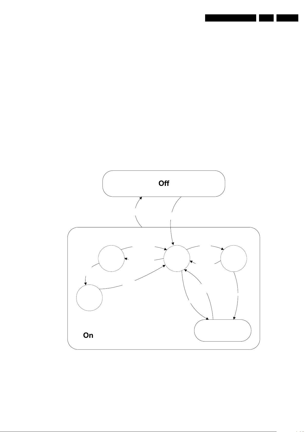
Semi
St by
St by
Mains
on
Mains
off
GoToProtection
-WakeUp requested
-Acquisition needed
-No data Acquisition
required
-tact SW pushed
-last status is hibernate
after mains ON
- St by requested
-tact SW pushed
WakeUp
requested
Protection
WakeUp
requested
(SDM)
GoToProtection
Hibernate
-Tact switch Pushed
-last status is hibernate
after mains ON
Tact switch
pushed
I_17660_124.eps
140308
EN 27Q529.1E LC 5.
Additional Info
• 12NC LVDS2DP board. Displays the 12NC of the built-in
LVDS-to-DisplayPort software.
• 12NC monitor board. Displays the 12NC of the monitor
board.
• SW version DPTX. Displays the built-in DisplayPort TX
software version.
• SW version DPRX. Displays the built-in DisplayPort RX
software version.
• SW version FPGA e-box. Displays the built-in FPGA ebox (HUB) software version.
• SW version FPGA monitor. Displays the built-in FPGA
monitor software version.
• SW version microP monitor. Displays the built-in monitor
microprocessor software version.
• SW version NVM monitor. Displays the built-in monitor
NVM software version.
How to Exit CSM
Press “MENU” on the RC-transmitter.
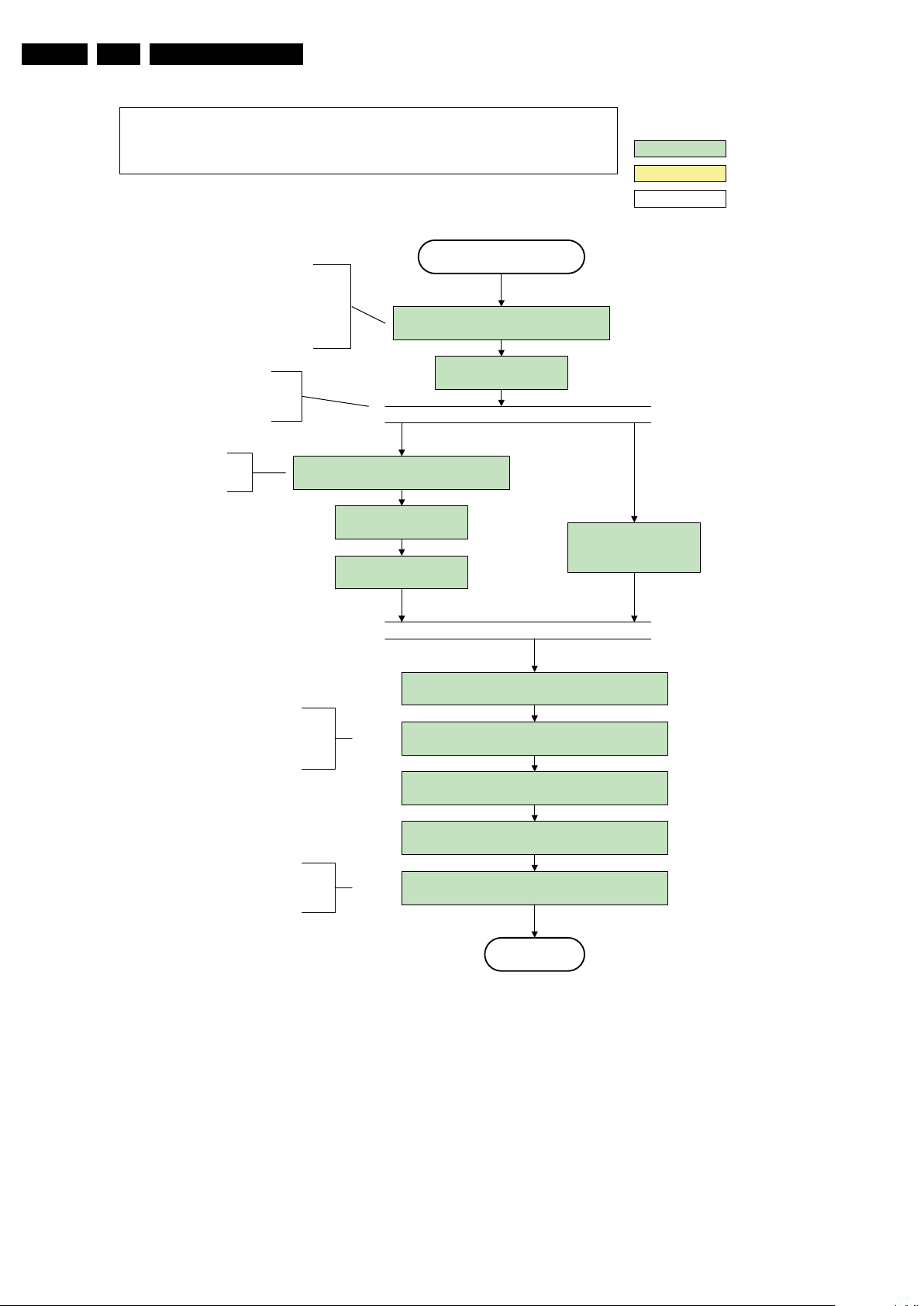
5.3 Stepwise Start-up
When the TV is in a protection state due to an error detected by
stand-by software (error blinking is displayed) and SDM is
activated via shortcutting the pins on the SSB, the TV starts up
until it reaches the situation just before protection. So, this is a
kind of automatic stepwise start-up. In combination with the
start-up diagrams below, you can see which supplies are
present at a certain moment. Important to know is, that if e.g.
the 3V3 detection fails and thus error layer 2 = 18 is blinking
while the TV is restarted via SDM, the Stand-by Processor will
enable the 3V3, but the TV set will not go to protection now.
The TV will stay in this situation until it is reset (Mains/AC
Power supply interrupted). Caution: in case the start up in this
mode with a faulty FET 7U08 is done, you can destroy all IC’s
supplied by the +3V3, due to overvoltage (12V on 3V3-line). It
is recommended to measure first the FET 7U08 or other FET’s
on shortcircuit before activating SDM via the service pads.
The abbreviations “SP” and “MP” in the figures stand for:
• SP: protection or error detected by the Stand-by
Processor.
• MP: protection or error detected by the MIPS Main
Processor.
Figure 5-3 Transition diagram
Page 28
EN 28 Q529.1E LC5.
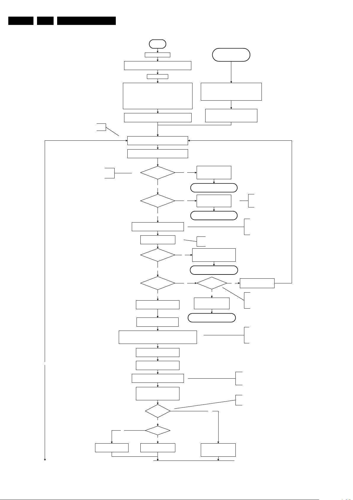
No
EJTAG probe
connected ?
No
Yes
Release AVC system r eset
Feed warm boot script
To I_17660_125b.eps To I_17660_125b.eps
Cold boot?
Yes
No
Set I²C slave address
of Standby µP to (A0h)
An EJTAG probe (e.g. WindPower ICE probe) can
be connected for Linux Kernel debugging
purposes.
This will a llow access to NVM a nd
NAND FLASH and can not be done
earlier because the FLASH needs to
be in Write Protect as long as the
supplies are not available.
Detect EJTAG debug probe
(pulling pin of the probe interface to
ground by inserting EJTAG probe)
Relea se AVC system r eset
Feed cold boot script
Release AVC system r eset
Feed initializing boot script
disable alive mechanism
Initialise I/O pins of the st-by µP:
- Switch reset-AVCLOW (reset state)
- Switch WP-NandFlash LOW (protected)
- Switch reset-system LOW (reset state)
- Switch reset-5100 LOW (reset state)
- Switch reset-Ethernet LOW (reset state)
- Switch reset-ST7100 LOW (reset state)
- keep reset-NVM high, Audio-reset and Audio-Mute-Up HIGH
Off
Standby Supply starts running.
All standby supply voltages become available .
st-by µ P resets
Stand by or
Protection
Mains is app lied
- Switch Audio-Reset high.
It is low in the standby mode if the standby
mode lasted longer than 10s.
start keyboard scanning, RC detection. Wake up reasons are
off.
If the protection state was left by short circuiting the
SDM pins, detection of a protection condition during
startup will stall the startup. Protection conditions in a
playing set will be ignored. The protection mode will
not be entered.
Switch LOW the RESET-NVM line to allow access to NVM. (Add a
2ms delay before trying to address the NVM to allow correct NVM
initialization, this is not issue in this setup, the delay is automatically
covered by the architectural setup)
Release Reset-PNX5100.
PNX5100 will start b ooting.
Wait 10ms (minimum) to allow the bootscript
of the PNX5100 to configure the PCI arbiter
Before PNX8541 boots, the PNX5100 should have
set its PCI arbiter (bootscript command). To allow
this, approx. 1ms is needed. This 1ms is extended
to 10ms to also give some relaxation to the supplies.
Switch HIGH the WP-NandFlash to
allow access to NAND Flash
+12V, +/-12Vs, AL and Bolt-on power
is switched on, followed by the +1V2 DCDC converter
Enable the supply fault detection
algorithm
No
Yes
Detect-1 I/O line
High?
Switch ON Platform and display supply by switching
LOW the Standby line.
This enables the +3V3 and
+5V converter. As a result,
also +5V-tuner, +2V5, +1V8PNX8541 and +1V8-PNX5100
become available.
yes
Enable the DCDC converter for +3V3 and
+5V. (EN ABLE-3V3)
Voltage output error:
Layer1: 2
Layer2: 18
Important remark; the appearance of the +12V
will start the +1V2 DCDC converter automatically
No
Yes
Supply-fault I/O
High?
The supply-fault line is a
combination of the DCDC
converters and the audio
protection line.
1V2 DCDC or class D error:
Layer1: 2
Layer2: 19
Enter protection
No
Detect2 high received
within 1 second?
Power-OK er ror:
Layer1: 3
Layer2: 16
Enter protection
Yes
No
Supply-fault I/O
High?
3V3 / 5V DCDC or class D error:
Layer1: 2
Layer2: 11
Enter protection
Wait 50ms
Enter protection
Delay of 50ms needed because of the latency of the detect-1 circuit.
This delay is also needed for the PNX5100. The reset of the
PNX5100 should only be released 10ms after powering the IC.
Detect2 should be polled on the standard 40ms
interval and startup should be continued when
detect2 becomes high.
Yes
No
Detect -2 I/ O line
High?
Disable 3V3, switch standby
line high and wait 4 seconds
Added to make the system more robust to
power dips during startup. At this point the
regular supply fault detection algorithm which
normally detects power dips is not up and
running yet.
I_17660_125a.eps
140308
Service Modes, Error Codes, and Fault Finding
Figure 5-4 “Off” to “Semi Stand-by” flowchart (part 1)
Page 29
Service Modes, Error Codes, and Fault Finding
Yes
MIPS reads the wake up reason
from standby µP.
Semi-Standby
initialize tuner, Master IF and channel
decoder
Initialize video processing IC's
Initiali ze source sele ction
initialize AutoTV by triggering CHS AutoTV Init interface
3-th try?
No
Blink Code as
error code
Bootscript ready
in 1250 ms?
Yes
No
Enable Alive check mechanism
Wait until AVC starts to
communicate
SW initializatio n
succeeded
within 20s?
No
Switch Standby
I/O line high.
RPC start (comm. protocol)
Set I²C slave address
of Standby µP to (60h)
Yes
Disable all supply related protections and
switch off the +3V3 +5V DC/DC converter.
switch off the remaining DC/DC
converters
Wait 5ms
Switch AVC PNX85 41
in reset (active low )
Wait 10ms
Switch the NVM reset
line HIGH.
Flash to Ram
image transfer succeeded
within 30s?
No
Yes
Code =
Layer1: 2
Layer2: 53
Code =
Layer1: 2
Layer2: 15
Initialize Ambilight with Lights off.
Timing need to be updated if
more mature info is available.
Timing needs to
be updated if more
mature info is
available.
Timing needs to be
updated if more
matur e info is
available.
Downloaded
successfully ?
Download firmware into the channel
decoder
Third try? No
No
Yes
Log channel decoder error:
Layer1: 2
Layer2: 37
Yes
Initialize audio
Enter protection
Release reset MPEG4 module:
BOLT-ON-IO: High
MPEG4 module will start booting
autonomously.
Wait 3000 ms
Start alive IIC polling
mechanism
POR polling positive?
yes
No
Log SW event:
STi7100PorFailure
Wait 200 ms
POR polling positive?yes
No
bootSTi7100PorFailure:
Log HW error
Layer1: 2
Layer2: 38
and generate cold boot
Alive
polling
Log SW event
STi7100AliveFailedError
and generate fast cold reboot
eventually followed by a cold
reboot.
NOK
Reset-system is switched HIGH by the
AVC at the end of the bootscript
AVC releases Reset-Ethernet when the
end of the AVC boot-script is detected
This cannot be done through the bootscript,
the I/O is on the standby µP
Reset- system is connected to USB
From I_17660_125a.eps From I_17660_125a.eps
-reset,
4to1HDMI Mux and channel decoder.
Reset-Audio and Audio-Mute-Up are
switched by MIPS code later on in the
startup process
Reset-syst em is switched HIGH by the
AVC at the end of the bootscript
AVC releases Reset-Ethernet when the
end of the AVC boot-script is detected
Reset-Audio and Audio-Mute-Up are
switched by MIPS code later on in the
startup process
Switch on the display in case of a LED backlight
display by sending the TurnOnDisplay(1) (I²C)
command to the PNX5100
In case of a LED backlight display, a LED DIM panel is
present which is fed by the Vdisplay. To power the LED DIM
Panel, the Vdisplay switch driven by the PNX5100 must be
closed. The display startup sequence is taken care of by the
LED DIM panel.
I_17660_125b.eps
140308
EN 29Q529.1E LC 5.
Figure 5-5 “Off” to “Semi Stand-by” flowchart (part 2)
Page 30
EN 30 Q529.1E LC5.
Service Modes, Error Codes, and Fault Finding
Constraints taken into account:
- Display may only be started when valid LVDS output clock can be delivered by the AVC .
- Between 5 and 50 ms after power is supplied, display should receive valid lvds clock .
- minimum wait time to switch on the lamp after power up is 200ms.
action holder: AVC
action holder: St-by
autonomous action
The assumption here is that a f ast toggle (<2s)
can only happen during ON-> SEMI -> ON. In
these states, the AVC is still act ive and can
provide the 2s delay. If the transitio n ON-> SEMI-
>STBY -> SEMI -> ON can be made in less than 2s,
the semi -> stby transition has to be delayed
CPipe already generates a valid output
clock in t he semi -standb y state : display
startup can start immediately when leaving
The timings to be used in
combination with the PanelON
comman d for t his specific display
The higher level requirement is that audio and
video should be demuted without transient
effects and that the audio should be demuted
maximum 1s before or at the same time as the
until the requirement is met.
the semi-standby state.
TurnOnDisplay(1) (I²C) command to the PNX5100
unblanking of the video.
Semi Standby
Wait until previous on-state is left more than 2
seconds ago. (to prevent LCD display problems)
Assert RGB video blanking
Switch on the display by sending the
wait 250ms (min. = 200ms)
Switch on LCD backlight
(Lamp-ON)
Wait until valid and stable audio and video , corresponding to
the requested output is delivered by the AVC.
Switch Audio -Reset low and wait 5ms
Release audio mute and wait 100ms before any other audio
handling is done (e.g. volume change)
and audio mute
Initialize audio and video
processing IC's and functions
according needed use case.
The higher level requirement is that the
ambilig ht functionality may not be switched on
before the backlight is turned on in case the
set contains a CE IPB inverter supply.
Figure 5-6 “Semi Stand-by” to “Active” flowchart
unblank the video.
Switch on the Ambilight functionality according the last status
settings.
Active
I_17660_126.eps
140308
Page 31

Service Modes, Error Codes, and Fault Finding
Active
Semi Standby
action holder: AVC
autonomous action
action holder: St-by
Initialize audio and video
processing IC's and functions
according needed use case.
Assert RGB video blanking
and audio mute
Wait until previous on-state is left more than 2
seconds ago. (to prevent LCD display problems)
The assumption here is that a f ast toggle (<2s)
can only happen during ON->SEMI ->ON. In
these states, the AVC is still act ive and can
provide t he 2s delay. If the t ransition ON -> SEMI-
->STBY-> SEMI -> ON can be made in less than 2s,
the semi - > stby transition has to be delayed
until the requirement is met.
Switch Audio-Reset low and wait 5ms
Constraints taken into account:
- Display may only be started when valid LVDS output clock can be delivered by the AVC .
- Between 5 and 50 ms after power is supplied, display should receive valid lvds clock .
- minimum wait time to switch on the lamp after power up is 200ms.
- To have a reliable operation of the backlight, the backlight should be driven with a PWM duty cycle of 100%
during the first second. Only after this first one or two seconds, the PWM may be set to the required output level
(Note that the PWM output should be present before the backlight is switched on). To minimize the artefacts, the
picture should only be unblanked after these first seconds.
Restore dimming backlight feature, PWM and BOOST output
and unblank the video.
Wait until valid and stable audio and video, corresponding to the requested
output is delivered by the AVC
AND
[the backlight PWM has been on for 1s (internal inverter LPL displays
OR the backlight PWM has been on for 2s (external inverter LPL displays)] .
The higher level requirement is that audio and
video should be demuted without transient
effects and that the audio should be demuted
maximum 1s before or at the same time as the
unblanking of the video.
Release audio mute and wait 100ms before any other audio
handling is done (e.g. volume change)
CPipe already generates a valid output
clock in t he semi -standby state: d isplay
startup can start immediately when leaving
the semi-standby state.
wait 250ms (min. = 200ms)
Switch on LCD backlight
(Lamp-ON)
Switch off the dimming backlight feature, set
the BOOST control to nominal and make sure
PWM output is set to 100%
Switch on the display by sending the
TurnOnDisplay(1) (I²C) command to the PNX5100
Switch on the Ambilight functionality according the last status
settings.
The higher level requirement is that the
ambilig ht functionality may n ot be swit ched on
before the backlight is turned on in case the
set contains a CE IPB inverter supply.
I_17660_127.eps
140308
EN 31Q529.1E LC 5.
Figure 5-7 “Semi Stand-by” to “Active” flowchart LCD with preheat
Page 32

EN 32 Q529.1E LC5.
Active
Semi Standby
action holder: AVC
autonomous action
action holder: St-by
Initialize audio and video
processing IC's and functions
according needed use case.
Assert RGB video blanking
and audio mute
Wait until previous on-state is left more than 2
seconds ago. (to prevent LCD display problems)
The assumption here is that a f ast toggle (<2s)
can only happen during ON-> SEMI -> ON. In
these states, the AVC is still active an d can
provide the 2s delay. If the transition ON -> SEMI-
>STBY->SEMI->ON can be made in less than 2s,
the semi -> stby transition has to be delayed
until the requirement is met.
Switch Audio -Reset low and wait 5ms
Constraints taken into account:
- Display may only be started when valid LVDS output clock can be delivered by the AVC.
- Between 5 and 50 ms after power is supplied, display should receive valid lvds clock .
- minimum wait time to switch on the lamp after power up is 200ms.
unblank the video.
Wait until valid and stable audio and video , corresponding to
the requested output is delivered by the AVC.
The higher level requirement is that audio and
video should be demuted without transient
effects and that the audio should be demuted
maximum 1s before or at the same time as the
unblanking of the video.
Release audio mute and wait 100ms before any other audio
handling is done (e.g. volume change)
CPipe already generates a valid output
clock in t he semi -standby state : display
startup can start immediately when leaving
the semi-standby state.
wait 250ms (min. = 200ms)
TBC in def. spec
Switch on LCD backlight
(Lamp-ON)
Switch on the display by sending the OUTPUTENABLE (I²C) command to the LED DIM panel
Switch on the Ambilight functionality according the last status
settings.
The higher level requirement is that the
ambilig ht functionality may n ot be swit ched on
before the backlight is turned on in case the
set contains a CE IPB inverter supply.
I_17660_128.eps
140308
Service Modes, Error Codes, and Fault Finding
Figure 5-8 “Semi Stand-by” to “Active” flowchart (LED backlight)
Page 33

Service Modes, Error Codes, and Fault Finding
Semi Standby
Active
action holder: AVC
autonomous action
action holder: St-by
Wait 25 0ms (min. = 200ms)
Mute all sound outputs via softmute
Mute all video outputs
switch off LCD backlight
Force ext audio outputs to ground
(I/O: audio reset)
And wait 5ms
Switch off the display by sending the
TurnOnDisplay(0) (I²C) command to the PNX5100
switch o ff Ambilight
Set main amplifier mute (I/O: audio-mute)
Wait 100ms
Wait until Ambilight has faded out
(fixed wait time of x s)
The higher level requirement is that the
backlight may not be switched off before the
ambilight functionality is turned off in case the
set contains a CE IPB inverter supply.
I_17660_129.eps
140308
EN 33Q529.1E LC 5.
Figure 5-9 “Active” to “Semi Stand-by” flowchart (LCD non DFI)
Page 34

EN 34 Q529.1E LC5.
transfer Wake up reasons to the Stand by µP.
Stand by
Semi Stand by
action holder: MIPS
autonomous action
action holder: St-by
Disable all supply related protections and switch off
the DC/DC converters (ENABLE-3V3)
Switch OFF all supplies by switching HIGH the
Standby I/O line
Switch AVC system in reset state
Switch reset-PNX5100 LOW
Switch reset-ST7100 LOW
Switch Reset-Ethernet LOW
Important remark:
release reset audio 10 sec after
entering st andby to save pow er
Wait 5ms
Wait 10ms
Switch the NVM reset line HIGH
Switch het WP-Nandflash LOW
Delay transition until ramping down of ambient light is
finished. *)
If ambientlight functionality was used in semi -standby
(lampadaire mode), switch off ambient light
*) If this is not performed and the set is
switched to standby when the switch off of
the ambilights is still ongoing , the lights will
switch off abruptly when the supply is cut.
Switch Memories to self-refresh (this creates a more
stable condition when switching off the power).
I_17660_130.eps
140308
Service Modes, Error Codes, and Fault Finding
Figure 5-10 “Semi Stand-by” to “Stand-by” flowchart
Page 35

Service Modes, Error Codes, and Fault Finding
Protection
action holder: MIPS
autonomous action
action holder: St-by
Redefine wake up reasons for protection
state and transfer to stand-by µP.
Log the appropriate err or and
set stand-by flag in NVM
MP
Ask stand-by µP to enter protection state
Flash the Protection-LED in order to indicate
protection state* (*): This can be the standby LED or the ON LED
depending on the availability in the set
SP
Switch off LCD lamp supply
Wait 250ms (min. = 200ms)
Switch off LVDS signal
Switch off 12V LCD supply within a time frame of
min. 0.5ms to max. 50ms after LVDS switch off.
If needed to speed up this transition,
this block could be omitted . This is
depending on the outcome of the
safety investiga tions .
Disable all supply related protections and switch off
the +1V8 and the +3V3 DC/DC converter.
Switch OFF all supplies by switching HIGH the
Standby I/O line.
Switch AVC in r eset state
Wait 5ms
Wait 10ms
Switch the NVM r eset line H IGH.
I_17660_131.eps
140308
EN 35Q529.1E LC 5.
Figure 5-11 “To Protection State” flowchart
5.4 Service Tools
5.4.1 ComPair
Introduction
ComPair (Computer Aided Repair) is a Service tool for Philips
Consumer Electronics products. and offers the following:
1. ComPair helps to quickly get an understanding on how to
repair the chassis in a short and effective way.
2. ComPair allows very detailed diagnostics and is therefore
capable of accurately indicating problem areas. No
knowledge on I
because ComPair takes care of this.
2
C or UART commands is necessary,
3. ComPair speeds up the repair time since it can
automatically communicate with the chassis (when the uP
is working) and all repair information is directly available.
4. ComPair features TV software up possibilities.
Specifications
ComPair consists of a Windows based fault finding program
and an interface box between PC and the (defective) product.
The ComPair II interface box is connected to the PC via an
USB cable. For the TV chassis, the ComPair interface box and
the TV communicate via a bi-directional cable via the service
connector(s).
The ComPair fault finding program is able to determine the
problem of the defective television, by a combination of
automatic diagnostics and an interactive question/answer
procedure.
Page 36

EN 36 Q529.1E LC5.
E_06532_036.eps
150208
TO
UART SERVICE
CONNECTOR
TO
UART SERVICE
CONNECTOR
TO
I2C SERVICE
CONNECTOR
TO TV
PC
HDMI
I
2
C only
Optional power
5V DC
ComPair II Developed by Philips Brugge
RC out
RC in
Optional
Switch
Power ModeLink/
Activity
I
2
C
ComPair II
Multi
function
RS232 /UART
Service Modes, Error Codes, and Fault Finding
How to Connect
This is described in the chassis fault finding database in
ComPair.
Figure 5-12 ComPair II interface connection
Caution: It is compulsory to connect the TV to the PC as
shown in the picture above (with the ComPair interface in
between), as the ComPair interface acts as a level shifter. If
one connects the TV directly to the PC (via UART), ICs will be
blown!
How to Order
ComPair II order codes:
• ComPair II interface: 3122 785 91020.
• Software is available via internet:
http://www.atyourservice.ce.philips.com
• ComPair UART interface cable for Q52x.x.
(using 3.5 mm Mini Jack connector): 3104 311 12742.
Note: While encounting problems, contact the local support
desk.
5.4.2 Memory and Audio Test
With this tool you can test the memory of the PNX8541, as well if the PNX5100 is enabled and audio-testing.
What is needed?
– An USB-stick.
– “TESTSCRIPT Q529” (3104 337 05021). Downloadable
from the Philips Service website from the section “Software
for Service only”.
– A ComPair/service cable (3104 311 12742)
Procedure
Create a directory “JETTFILES” under the root of the USB-stick
– Place “MemoryTestPNX8635.bin” and “autojett.bin”
(available in “TESTSCRIPT Q529”) under the directory
“JETTFILES”
– Install the computer program “BOARDTESTLOGGER”
(available in “TESTSCRIPT Q529”) on the PC
– Connect a “ComPair/service”-cable from the service-
connector in the set to the COM1-port of the PC
– Start-up the program “BOARDTESTLOGGER” and select
“COM1”
– Put the USB stick into the TV and startup the TV while
pressing the “i+”-button on a Philips DVD RC6 remote
control (it’s also possible to use a TV remote in “DVD”mode)
– On the PC the memory test is shown now. This is also
visible on the TV screen.
– In “BOARDTESTLOGGER” an option “Send extra UART
command” can be found where you can select “AUD1”.
This command generates hear test tones of 200, 400,
1000, 2000, 3000, 5000, 8000 and 12500Hz.
5.4.3 LVDS Tool
Support of this LVDS Tool has been discontinued.
5.5 Error Codes
5.5.1 Introduction
The error code buffer contains all detected errors since the last
time the buffer was erased. The buffer is written from left to
right, new errors are logged at the left side, and all other errors
shift one position to the right.
When an error occurs, it is added to the list of errors, provided
the list is not full. When an error occurs and the error buffer is
full, then the new error is not added, and the error buffer stays
intact (history is maintained).
To prevent that an occasional error stays in the list forever, the
error is removed from the list after more than 50 hrs. of
operation.
When multiple errors occur (errors occurred within a short time
span), there is a high probability that there is some relation
between them.
Below the way errors will be displayed on the HUB:
• There is a simple blinking LED procedure for board level
repair (home repair) so called LAYER 1 errors next to the
existing errors which are LAYER 2 errors.(see table 5-2
error code overview).
– LAYER 1 errors are one digit errors.
– LAYER 2 errors are 2 digit errors.
• In protection mode.
– From consumer mode: LAYER 1.
– From SDM mode: LAYER 2.
• Fatal errors, if I2C bus is blocked and the set reboots,
CSM and SAM are not selectable.
– From consumer mode: LAYER 1.
– From SDM mode: LAYER 2.
Important remark:
For all errors detected by MIPS which are fatal =>
rebooting of the TV set (reboot starts after LAYER error
1 blinking), one should short the solder paths at startup from the power OFF state by mains interruption and
not via the power button to trigger the SDM via the
hardware pins.
• In CSM mode
– When entering CSM: error LAYER 1 will be displayed
by blinking LED. Only the latest error is shown.
• In SDM mode
– When SDM is entered via Remote Control code or the
hardware pins, LAYER 2 is displayed via blinking LED
on the HUB.
• In the ON state
– In “Display error mode”, set with the RC commands
“mute_06250X _OK” LAYER 2 errors are displayed via
blinking LED on the HUB.
• Error display on screen.
– In CSM no error codes are displayed on screen.
– In SAM the complete error list from the HUB only is
shown!
Basically there are three kinds of errors:
• Errors detected by the Stand-by software which lead to
protection. These errors will always lead to protection and
an automatic start of the blinking LED (HUB) LAYER error
1.(see section “5.6 The Blinking LED Procedure”).
• Errors detected by the Stand-by software which not
lead to protection. In this case the LED from the HUB
should blink the involved error. See also section “5.5 Error
Codes, 5.5.4 Error Buffer, Extra Info”. Note that it can take
Page 37

Service Modes, Error Codes, and Fault Finding
up several minutes before the TV starts blinking the error
(e.g. LAYER error 1 = 2, LAYER error 2 = 15 or 53).
• Errors detected by main software (MIPS). In this case
the error will be logged into the error buffer and can be read
out via ComPair, via blinking LED method LAYER error 12, or in case picture is visible, via SAM.
Important remark :
Errors on the monitor are displayed by blinking LED only during
the start up.They will be displayed only once or twice.
5.5.2 How to Read the Error Buffer
Use one of the following methods:
• On screen via the SAM (only when a picture is visible).
E.g.:
– 00 00 00 00 00: No errors detected
– 23 00 00 00 00: Error code 23 is the last and only
detected error.
– 37 23 00 00 00: Error code 23 was first detected and
error code 37 is the last detected error.
– Note that no protection errors can be logged in the
error buffer.
• Via the blinking LED procedure. See section 5.5.3 How to
Clear the Error Buffer.
•Via ComPair.
EN 37Q529.1E LC 5.
5.5.3 How to Clear the Error Buffer
Use one of the following methods:
• By activation of the “RESET ERROR BUFFER” command
in the SAM menu.
• With a normal RC, key in sequence “MUTE” followed by
“062599” and “OK”.
• If the content of the error buffer has not changed for 50+
hours, it resets automatically.
5.5.4 Error Buffer
In case of non-intermittent faults, clear the error buffer before
starting to repair (before clearing the buffer, write down the
content, as this history can give significant information). This to
ensure that old error codes are no longer present.
If possible, check the entire contents of the error buffer. In
some situations, an error code is only the result of another error
code and not the actual cause (e.g. a fault in the protection
detection circuitry can also lead to a protection).
There are several mechanisms of error detection:
• Via error bits in the status registers of ICs.
• Via polling on I/O pins going to the stand-by processor.
• Via sensing of analog values on the stand-by processor or
the PNX8541.
• Via a “not acknowledge” of an I
Take notice that some errors need several minutes before they
start blinking or before they will be logged. So in case of
problems wait 2 minutes from start-up onwards, and then
check if the front LED is blinking or if an error is logged.
2
C communication.
Page 38

EN 38 Q529.1E LC5.
Table 5-2 Error code overview
Service Modes, Error Codes, and Fault Finding
Description Layer 1 Layer 2
2
I
C3 2 13 MIPS E BL / EB SCL/D-SSB SSB
2
C4 5 14 MIPS E BL / EB SCL/D-DISP Display (LED back light only)
I
by
PNX doesn’t boot (HW cause) 2 15 Stby µP E BL PNX8541 I
Monitored
Error/
Error Buffer/
Prot
Blinking LED Device Defective Board
2
C blocked SSB
12V 3 16 Stby µP P BL / Supply
1V2, 3V3, 5V to low 2 18 Stby µP P BL / SSB
1V2 or Class D 2 19 Stby µP P BL / SSB
3V3/5V DCDC to high 2 11 Stby µP P BL / SSB
Temp protection 3 12 MIPS P BL/EB / SSB
PNX 5100 2 21 MIPS E EB PNX5100 SSB
HDMI mux 2 23 MIPS E EB AD8197A SSB
2
C switch 2 24 MIPS E EB PCA9540 SSB
I
Master IF 2 26 MIPS E EB TDA9898 SSB
FPGA Ambilight 2 28 MIPS E EB / SSB
Tuner 2 34 MIPS E EB UV1783S/TD1716 SSB
Channel Decoder DVB-T 2 37 MIPS E EB TDA10048 SSB
ST7100 2 38 MIPS E EB ST7100 SSB
FAN I2C expander 7 41 MIPS E EB PCA 9533 SSB
T° sensor 7 42 MIPS E EB LM 75 SSB
FAN 7 43/44 MIPS E EB / FAN
main NVM 2 / MIPS E X STM24C128 SSB
Channel decoder DVB-C 2 48 MIPS E EB TDA 10023 SSB
PNX doesn’t boot (SW cause) 2 53 Stby µP E BL PNX8541 SSB
DP Tx 6 54 MIPS E EB GM60028 LVDS2DP
FPGA LVDS Rx 6 55 MIPS E EB
DP port not connected 5 56 MIPS E EB DP cable/monitor /
Extra Info
• Rebooting. When a TV is constantly rebooting due to
internal problems, most of the time no errors will be logged
or blinked. This rebooting can be recognized via a ComPair
interface and Hyperterminal (for Hyperterminal settings,
see section “5.8 Fault Finding and Repair Tips, 5.8.6
Logging). It’s shown that the loggings which are generated
by the main software keep continuing. In this case
diagnose has to be done via ComPair.
• Error 11 (3V3/5V too high). This protection can occur
during start up (LAYER error 1 = 2). Be careful to overrule
this protection via SDM for the reason supply related
devices can be possibly destroyed here.
• Error 12 (Temp protection). Current situation: when
temperature rises above limit inside the HUB, the
protection is triggered and the TV set is switched “OFF”. No
indication will be displayed on the LED of the HUB, yet
error layer = 12 is logged and will be displayed when SDM
is active.
• Error 13 (I
2
C bus 3 blocked). At the time of release of this
manual, this error was not working as expected. Current
situation: when this error occurs, the TV will constantly
reboot due to the blocked bus. The best way for further
diagnosis here, is to use ComPair.
• Error 15 (PNX8541 doesn’t boot). Indicates that the main
processor was not able to read his bootscript. This error will
point to a hardware problem around the PNX8541
(supplies not OK, PNX 8541 completely dead, I
between PNX and Stand-by Processor broken, etc...).
When error 15 occurs it is also possible that I
blocked (NVM). I
2
C2 can be indicated in the schematics as
2
C link
2
C2 bus is
follows: SCL-UP-MIPS, SDA-UP-MIPS, SCL-2 or SDA-2.
Other root causes for this error can be due to hardware
problems with : NVM PNX5100, PNX5100 itself, DDR’s.
• Error 16 (12V). This voltage is made in the power supply
of the HUB and results in protection (LAYER error 1 = 3) in
case of absence. When SDM is activated we see blinking
LED LAYER error 2 = 16.
• Error 18 (1V2-3V3-5V too low). All these supplies are
generated by the DC/DC supply on the SSB. If one of these
supplies is too low, protection occurs and blinking LED
LAYER error 1 = 2 will be displayed automatically. In SDM
this gives LAYER error 2 = 18.
• Error 19 (1V2 or class D). If one of the 1V2 supplies is too
high or too low in the start up procedure the supply fault
becomes low.
• Error 21 (PNX 5100). At the time of release of this manual,
this error was not working as expected. Current situation:
when there is no I
2
C communication towards the PNX5100
after startup (power off by disconnection of the mains
cord), LAYER error 2 will blink continuously via the blinking
LED procedure in SDM. (startup the TV with the solder
paths short to activate SDM).
• Error 23 (HDMI). When there is no I
2
C communication
towards the HDMI mux after start up, LAYER error 2 = 23
will be logged and displayed via the blinking LED
procedure if SDM is switched on.
• Error 26 (Master IF). When there is no I
2
C communication
towards the Master IF after start up, LAYER error 2 = 26
will be logged and displayed via the blinking LED
procedure when SDM is switched on.
• Error 28 (FPGA ambilight). When there is no I
2
C
communication towards the FPGA ambilight after start up,
LAYER error 2 = 28 will be logged and displayed via the
blinking LED procedure if SDM is switched on. Note that it
can take up several minutes before the TV starts blinking
LAYER error 1 = 2 in CSM or in SDM, LAYER error 2 = 28.
• Error 34 (Tuner). When there is no I
2
C communication
towards the tuner after start up, LAYER error 2 = 34 will be
logged and displayed via the blinking LED procedure when
SDM is switched on.
• Error 37 (Channel decoder DVBT). When there is no I
2
communication towards the DVBT channel decoder after
start up, LAYER error 2 = 37 will be logged and displayed
via the blinking LED procedure if SDM is switched on.
• Error 38 (STI7100). When there is no I
2
C communication
towards the STI7100 after startup (power off by
C
Page 39

Service Modes, Error Codes, and Fault Finding
EN 39Q529.1E LC 5.
disconnection of the mains cord), LAYER error 2 = 38 will
be logged and displayed via the blinking LED procedure in
SDM (startup the TV with the solder paths short to activate
SDM). Remark : if the error occurs during the ON state, the
TV will constantly reboot and no LED blinking will be
displayed. This rebooting can be recognized via a ComPair
interface and Hyperterminal (for Hyperterminal settings,
see section “5.8 Fault Finding and Repair Tips, 5.8.6
Logging”). It is shown that the loggings which are
generated by the main software keep continuing. Check in
the logging for keywords like e.g. “Device error 38”.
• Main NVM HUB. When there is no I
2
C communication
towards the main NVM, LAYER error 1 = 2 will be
displayed via the blinking LED procedure. In SDM, LAYER
error 2 can be 19 here. Check the logging for keywords like
2
“I
C bus blocked”.
• Error 42 (Temperature sensor). At the time of release of
this manual, this error was not working as expected.
Current situation: when this error occurs, the TV will
endlessly reboot due to the blocked bus. The best way for
further diagnosis here, is to use ComPair or check the
logging.
• Error 48 (Channel decoder DVBC). When there is no I
2
communication towards the DVBC channel decoder after
start up, LAYER error 2 = 48 will be logged and displayed
via the blinking LED procedure while SDM is active.
• Error 53. This error will indicate that the PNX8541 has
read his bootscript (when this would have failed, error 15
would blink) but initialization was never completed because
of hardware problems (NAND flash, ...) or software
initialization problems. Possible cause could be that there
is no valid software loaded (try to upgrade to the latest main
software version). Note that it can take up to 2 minutes
before the TV starts blinking LAYER error 1 = 2 or in SDM,
LAYER error 2 = 53.
• Error 55 (FPGA LVDS Rx). At the time of release of this
manual, this error was not working as expected. Current
situation: When there is no I2C communication towards the
LVDS2DP panel, the TV set will start rebooting and no
blinking on the hub will be displayed. The reset-start spacer
is displayed on the monitor LED once in a while as start of
the error blinking but none are logged. Because no picture
is available, the only way to detect failure on the FPGA
device is to check in the logging from the hub (via service
connector hub) prints as: “setting lvdsrx output enable to 1,
was 0”. This betrays the failure of the FPGA LVDS Rx.
5.5.5 Monitor Errors for Essence
When an error of the monitor appears, it is displayed by a
blinking LED on the monitor triggered via the acknowledge of
C
the failing device. This is only once or twice. When the error
dissappears or when the I2C command is not repeated, the
blinking LED stops. Resetting the errors of the monitor is not
possible via the item “clear errors” in SAM and can not be read
out either in the error buffer, they only will be displayed via
blinking LED during start-up.
Table 5-3 Start-up errors Essence
Defect Action Error on E-box Error on monitor
Supply cable and DP cable
unplugged
Supply cable and DP cable
unplugged
Supply cable unplugged Start up with mains cord
Supply cable unplugged Start up from Standby
DP cable unplugged Start up with mains cord
DP cable unplugged Start up from Standby
E-box defect Supply fault Blinking LED error 3
E-box defect SSB defect, DP initialized Blinking LED error 2
Start up with mains cord
or tact switch (HUB)
Start up from Standby
with RC6 (monitor)
or tact switch (HUB)
with RC6 (monitor)
or tact switch (HUB)
with RC6 (monitor)
Blinking LED error 5
No LED
Logging error 56 (layer 2)
No reaction No LED and no RC6
blinking
Blinking LED error 5
Standby
Logging error 56 (layer 2)
Blinking LED error 5
Logging error 56 (layer 2)
Blinking LED error 5
RC6 blinking, Standby
LED, no error
No picture, no error
Logging error 56 (layer 2)
No RC 6 blinking
No picture, no error
Standby
if no 24V : Standby
Logging error layer 2 if
possible
24V=OK : no picture, no
error
No error
Logging error layer 2
E-box defect SSB defect, DP not
initialized
E-box defect DP boar defect Blinking LED error 6
Blinking LED error 2
Logging error layer 2
No picture, no error
No picture, no error
Logging error layer 2
Monitor defect FPGA No error Blinking LED error 2
Logging error 2
Monitor defect 3V3 monitor Blinking LED error 5
Logging error 56 (layer 2)
Monitor defect 12V monitor Blinking LED error 5
Logging error 56 (layer 2)
Monitor defect DP port defect Blinking LED error 5
Blinking LED error 3
Logging error 3
Blinking LED error 4
Logging error 4
No picture, no error
Logging error 56 (layer 2)
Monitor defect DP RX Blinking LED error 5
Logging error 56 (layer 2)
Blinking LED error 6
Logging error 6
Monitor defect NVM No error Blinking LED error 7, No
logging possible
Extra Info
• At the time of release of this manual, errors as mentioned
above in table 5-3 can possibly not fully work as expected
due to unresolved software bugs.
Page 40

EN 40 Q529.1E LC5.
Service Modes, Error Codes, and Fault Finding
5.6 The Blinking LED Procedure
5.6.1 Introduction
The blinking LED procedure can be split up into two situations:
• Blinking LED procedure LAYER error 1. In this case the
error is automatically blinked when the TV is put in CSM.
This will be only one digit error, namely the one that is
referring to the defective board (see table “Table 5-2 Error
code overview”) which causes the failure of the TV. This
approach will especially be used for home repair and call
centres. The aim here is to have service diagnosis from a
distance.
• Blinking LED procedure LAYER error 2. Via this procedure,
the content of the error buffer can be made visible via the
front LED of the HUB. In this case the error contains
2 digits (see table “Table 5-2 Error code overview”) and will
be displayed when SDM (hardware pins) is activated. This
is especially useful for fault finding and gives more details
regarding the failure of the defective board.
Important remark:
For all errors detected by MIPS which are fatal =>
rebooting of the TV set (reboot starts after LAYER error 1
blinking), one should short the solder paths at start-up from
the power OFF state by mains interruption and not via the
power button to trigger the SDM via the hardware pins.
When one of the blinking LED procedures is activated, the front
LED of the HUB will show (blink) the content of the error buffer.
Error codes greater then 10 are shown as follows:
1. “n” long blinks (where “n” = 1 to 9) indicating decimal digit
2. A pause of 1.5 s
3. “n” short blinks (where “n”= 1 to 9)
4. A pause of approximately 3 s,
5. When all the error codes are displayed, the sequence
finishes with a LED blink of 3 s
6. The sequence starts again.
Example: Error 12 8 6 0 0.
After activation of the SDM, the front LED will show:
1. One long blink of 750 ms (which is an indication of the
decimal digit) followed by a pause of 1.5 s
2. Two short blinks of 250 ms followed by a pause of 3 s
3. Eight short blinks followed by a pause of 3 s
4. Six short blinks followed by a pause of 3 s
5. One long blink of 3 s to finish the sequence
6. The sequence starts again.
5.6.2 How to Activate
Use one of the following methods:
• Activate the CSM. The blinking front LED of the HUB will
show only the latest layer error 1, this works in “normal
operation” mode or automatically when the error/protection
is monitored by the standby processor. At the time of this
release, this layer error 1 blinking was not working as
expected.
In case no picture is shown and there is no LED blinking,
read the logging to detect whether “error devices” are
mentioned. (see section “5.8 Fault Finding and Repair
Tips, 5.8.6 Logging”).
• Activate the SDM. The blinking front LED of the HUB will
show the entire contents of the layer error 2 buffer, this
works in “normal operation” mode or when SDM (via
hardware pins) is activated when the tv set is in protection.
Important remark:
For all errors detected by MIPS which are fatal =>
rebooting of the TV set (reboot starts after LAYER error 1
blinking), one should short the solder paths at start up from
the power OFF state by mains interruption and not via the
power button to trigger the SDM via the hardware pins.
• Transmit the commands “MUTE” - “062500” - “OK”
with a normal RC. The complete error buffer is shown.
Take notice that it takes some seconds before the blinking
LED starts.
• Transmit the commands “MUTE” - “06250x” - “OK”
with a normal RC (where “x” is a number between 1
and 5). When x = 1 the last detected error is shown, x = 2
the second last error, etc.... Take notice that it takes some
seconds before the blinking LED starts.
5.7 Protections
5.7.1 Software Protections
Most of the protections and errors use either the stand-by
microprocessor or the MIPS controller as detection device.
Since in these cases, checking of observers, polling of ADCs,
and filtering of input values are all heavily software based,
these protections are referred to as software protections.
There are several types of software related protections, solving
a variety of fault conditions:
• Protections related to supplies: check of the 12V, +5V,
+3V3 and 1V2.
• Protections related to breakdown of the safety check
mechanism. E.g. since the protection detections are done
by means of software, failing of the software will have to
initiate a protection mode since safety cannot be
guaranteed any more.
Remark on the Supply Errors
The detection of a supply dip or supply loss during the normal
playing of the set does not lead to a protection, but to a cold
reboot of the set. If the supply is still missing after the reboot,
the TV will go to protection.
Protections during Start-up
During TV start-up, some voltages and IC observers are
actively monitored to be able to optimize the start up speed,
and to assure good operation of all components. If these
monitors do not respond in a defined way, this indicates a
malfunction of the system and leads to a protection. As the
observers are only used during start up, they are described in
the start up flow in detail (see section “5.3 Stepwise Start-up”).
5.7.2 Hardware Protections
The only real hardware protection in this chassis appears in
case of an audio problem e.g. DC voltage on the speakers. The
DC check circuit pulls the “A-STBY” line low and will paralize
the Class-D audio.
5.7.3 Important remark regarding the blinking LED indication
As for the blinking LED indication, the blinking of error layer 1
can be switched off by pushing the power button on the
keyboard.
This condition is not valid after the set was unpowered (via
mains interruption). The blinking LED starts again and can only
be switched off by unplugging the mains connection.
This can be explained by the fact that the MIPS can not load
the keyboard functionality from software during the start up and
doesn’t recognizes the keyboard commands at this time.
Page 41

Service Modes, Error Codes, and Fault Finding
EN 41Q529.1E LC 5.
5.8 Fault Finding and Repair Tips
Read also section “5.5 Error Codes, 5.5.4 Error Buffer, Extra
Info”.
5.8.1 Audio Amplifier
The Class D-IC 7D10 has a powerpad for cooling. When the IC
is replaced it must be ensured that the powerpad is very well
pushed to the PCB while the solder is still liquid. This is needed
to insure that the cooling is guaranteed, otherwise the Class DIC could break down in short time.
5.8.2 CSM
When CSM is activated and there is a USB stick connected to
the TV, the software will dump the complete CSM content to the
USB stick. The file (CSM.txt) will be saved in the root of the
USB stick. If this mechanism works it can be concluded that a
large part of the operating system is already working (MIPS,
USB...)
5.8.3 DC/DC Converter
Introduction
The onboard supply consists of 5 DC/DC converters and 7
linear stabilizers. The DC/DC converters have all +12V input
voltage and deliver:
1. +1V2-PNX8541 supply voltage, stabilised close to
PNX8541 chip.
2. +1V2-PNX5100 supply voltage, stabilised close to
PNX5100 chip.
3. +3V3 (overall 3.3 V for onboard IC’s).
4. +5V for USB and Conditional Access Interface and +5V5TUN tuner stabilizer.
5. +33VTUN for analogue only tuners (AP diversity).
The linear stabilizers are providing:
1. +1V supply voltage (out of +1V2-PNX8541), stabilized
close to ST7101 chip (MPEG4 diversity).
2. +1V8-PNX5100.
3. +1V8-PNX8541 (reserved because +1V8-PNX5100 used
also for DDR2 interface of PNX8541 via 5FB0).
4. +2V5 (MPEG4 diversity).
5. +1V2-STANDBY (out of +3V3-STANDBY).
6. +5V-TUN (out of +5V5-TUN).
7. +3V3-STANDBY (out of +12V, reserved).
+3V3-STANDY and +1V2-STANDBY are permanent voltages.
Supply voltages +1V2-PNX8541, +1V2-PNX5100 and +1V are
started immediately when +12V incoming voltage is available
(+12V is enabled by STANDBY signal, active low). Supply
voltages +3V3, 2V5, +1V8-PNX5100, +1V8-PNX8541, +5V
and +5V-TUN are switched-on directly by signal ENABLE-3V3
(active low) when +12V and previous mentioned voltages are
all available.
Debugging
The best way to find a failure in the DC/DC converters is to
check their starting-up sequence at power-on via the mains
cord, presuming that the standby microprocessor and the
external supply are operational. Take STANDBY signal highto-low transition as reference.
When +12V rises above 10V then +1V2-PNX8541, +1V2PNX5100 and +1V are started immediately. Then, after
ENABLE-3V3 goes low, all the other supply voltages should
rise within 10 ms. Boost voltages should be OK when +1V2PNX8541, +1V2-PNX5100 are available (FU07 and FU8A,
around 19V).
SUPPLY-FAULT signal should be high when all supply
voltages are started-up.
Tips
• Usually, when supply voltage is short-circuited to GND, the
corresponding DC/DC converter is making audible noise.
• The drop voltage across resistors 3U70 and 3U3T is
100 mV to 2000 mV.
• Defective (in short-circuit) power MOS-FET’s lead usually
to their controller IC broken; if one or more high-side MOSFET’s (7U05, 7U08, 7U0D-1 or 7U0H-1) is broken then the
platform can be heavily damaged if started in SDM-mode
(SUPPLY-FAULT signal is then ignored, while higher than
normal supplies will be generated).
• The +33VTUN generator circuit (7U0P + 7U0Q +
surrounding components) has low output current
capability. In case of too low or no output voltage check
transistor 7U0P (gate voltage pulses of about 10 V
amplitude and drain voltage pulses of about 35 V
amplitude) and the load (not more than 4.5 mA).
• High output ripple voltage of DC/DC converters can be
caused by defective (cracked or bad soldered) ceramic
capacitors in the feedback (DC or AC) input or output
filtering.
5.8.4 Exit “Factory Mode”
When an “F” is displayed in the screen's right corner, this
means that the set is in “Factory” mode, and it normally
happens after a new SSB has been mounted.
To exit this mode, push the “VOLUME minus” button on the
TV's local keyboard control for 10 seconds (this disables the
continuous mode).
Now push the “MENU” button for 10 seconds untill the “F”
disappears from the screen.
5.8.5 FAN selftest
A FAN-selftest can be done by pushing the red coloured button
on the remote control while the TV set is in CSM. Fore further
details, exit CSM and check the status of the FAN in the error
buffer via SAM (062596 + info button on the remote control). In
case of failure, the corresponding errors are displayed in the
error buffer (error 41,42,43, 44).
5.8.6 Logging
When something is wrong with the TV set (f.i.the set is
rebooting) you can check for more information via the logging
in Hyperterminal. The Hyperterminal is available in every
Windows application via Programs, Accessories,
Communications, Hyperterminal. Connect a “ComPair UART”cable (3104 311 12742) from the service connector in the TV
set to the “COM1”-port of the PC. After start-up of the
Hyperterminal, fill in a name (f.i. “logging”) in the “Connection
Description” box, then apply the following settings:
1. COM1
2. Bits per second = 38400
3. Data bits = 8
4. Parity = none
5. Stop bits = 1
6. Flow control = none
During the start-up of the TV set, the logging will be displayed.
This is also the case during rebooting of the TV set (the same
logging appears time after time). Also available in the logging
is the “Display Option Code” (useful when there is no picture),
look for item “DisplayRawNumber” in the beginning of the
logging. Tip: when there is no picture available during rebooting
you are able to check for “error devices” in the logging (LAYER
2 error) which can be very helpful to determine the failure cause
of the reboot. For protection state, there is no logging.
Page 42

EN 42 Q529.1E LC5.
I_18020_145.eps
190908
X530EDID1
X530EDID2
X530EDID3
5.8.7 Loudspeakers
Make sure that the volume is set to minimum during
disconnecting the speakers in the ON-state of the TV. The
audio amplifier can be damaged by disconnecting the speakers
during ON-state of the set! Sometimes the set can go into
protection, but that is not always the case.
5.8.8 Tuner
Attention: In case the tuner is replaced, always check the tuner
options!
5.8.9 UI over PCI bus
The UI is not integrated in the RGB signal but is sent from
PNX8541 to PNX5100 via the PCI bus. TXT and MHEG are
integrated in the RGB signal. So when TXT signal is available
but no UI, check the PCI bus.
5.8.10 Display option code
Attention: In case the SSB is replaced, always check the
display option code in SAM, even when picture is available.
Performance with the incorrect display option code can lead to
unwanted side-effects for certain conditions.
Service Modes, Error Codes, and Fault Finding
5.8.11 Upgrade EDID NVM
To upgrade the EDID NVM pin 7 of the EDID NVM has to be
short circuited to ground. Therefore some test points are
foreseen (figure “EDID-NVM pins”). See ComPair for further
instructions.
Figure 5-13 EDID-NVM pins
5.8.12 SSB Replacement
Follow the instructions in the flowchart in case a SSB has to be
exchanged. See figure “SSB replacement flowchart”.
Page 43

Service Modes, Error Codes, and Fault Finding
START
Create “r epair” directory on USB stick and
connect USB stick to TV-set
Go to SAM mode and save the TV settings
via “Upload to USB”.
Set is still
operating?
- Replace SSB board by a Service SSB.
- Make the SSB fit mechanically to the set.
Go to SAM mode, and reload settings
via “Download from USB”.
Saved settings
on USB stick?
Program “Display Option” code via 062598
MENU, followed by 3 digits code (this code
can be found on a sticker inside the set).
Check and perform alignments in SAM
according to the Service Manual.
E.g. option codes, colour temperature...
Connect PC via ComPair interface to Service
connector.
END
Yes
After entering “Display Option” code, set is
going to Standby (= validation of code).
Restart the set.
In case of settings reloaded from USB , the set type ,
serial number , Di splay 12 NC, are automaticall y stored
when enter ing dis play opti ons .
No
- C heck if corr ect “D ispl ay Option” code is pr ogram med .
- Ver ify “ Option C odes” ac cordi ng stick er ins ide the set .
- D efault set tings for Whi te driv e ... see Servi ce Manual
No
Set is sta rting up & displa y is OK .
If not already done;
Check latest software on Service website.
Update Main and Standby software via USB.
Q52xE SSB Board swap – v3
VDS/JA Updated 17-10-2008
Set is sta rting up but no dis play .
Final check of all menus in CSM.
Special attention for HDMI Keys.
Program “set type number”, “serial number”,
and “display 12NC”.
Update main software in this step, by using
“autorun.upg” file.
Start TV in Jett mode (DVD i+ (OSD))
Open ComPair browser Q52x.
Noisy picture with bands/lines is visible and the
red LED is continuous “on”
(sometimes also the letter “F” is visible).
Press 5 s. the “Volume minus” button on the local
cntrl until the red LED switches “off”, and then
press 5 s. the MENU button of the local cntrl.
The picture noise is replaced by blue mute!
Unplug the mainscord to verify the correct
disabling of the factory-mode.
Program “Display Option” code via 062598 MENU,
followed by 3 digits code (this code can be found
on a sticker inside the set ).
After entering “Display Option” code, set is going
to Standby (= validation of code).
Restart the set.
Set is sta rting up in “Fa ctory” mode .
Start-up set.
Set behaviour?
H_16771_007.eps
171008
EN 43Q529.1E LC 5.
Figure 5-14 SSB replacement flowchart
Page 44

EN 44 Q529.1E LC5.
Service Modes, Error Codes, and Fault Finding
5.9 Software Upgrading
5.9.1 Introduction
The set software and security keys are stored in a NANDFlash, which is connected to the PNX8541 via the PCI bus.
It is possible for the user to upgrade the main software via the
USB port. This allows replacement of a software image in a
stand alone set, without the need of an E-JTAG debugger. A
description on how to upgrade the main software can be found
in the DFU.
Important: When the NAND-Flash must be replaced, a new
SSB must be ordered, due to the presence of the security keys!
(copy protection keys, MAC address, ...). It is however also
possible to replace the NAND-Flash with a good one from a
scrap-board.
Perform the following actions after SSB replacement:
1. Set the correct option codes (see sticker inside the TV).
2. Update the TV software (see the DFU for instructions).
3. Perform the alignments as described in chapter 8 (section
“Reset of Repaired SSB”).
4. Check in CSM if the HDMI keys are valid.
For the correct order number of a new SSB, always refer to the
Spare Parts list!
5.9.2 Main Software Upgrade
• The “UpgradeAll.upg” file is only used in the factory.
• The “FlashUtils.upg” file is only used by service centra
which are allowed to do component level repair on the
SSB.
Automatic Software Upgrade
In “normal” conditions, so when there is no major problem with
the TV, the main software and the default software upgrade
application can be upgraded with the “AUTORUN.UPG”
(FUS part of the one-zip file: e.g. 3104 337 04731 _FUS
_Q591E_ 1.25.5.0_commercial.zip). This can also be done by
the consumers themselves, but they will have to get their
software from the commercial Philips website or via the
Software Update Assistant in the user menu (see DFU). The
“autorun.upg” file must be placed in the root of the USB stick.
How to upgrade:
1. Copy “AUTORUN.UPG” to the root of the USB stick.
2. Insert USB stick in the set while the set is in ON MODE.
The set will restart and the upgrading will start
automatically. As soon as the programming is finished, a
message is shown to remove the USB stick and restart the
set.
Manual Software Upgrade
In case that the software upgrade application does not start
automatically, it can also be started manually.
How to start the software upgrade application manually:
1. Disconnect the TV from the Mains/AC Power.
2. Press the “OK” button on a Philips TV remote control or a
Philips DVD RC-6 remote control (it is also possible to use
a TV remote in “DVD” mode). Keep the “OK” button
pressed while reconnecting the TV to the Mains/AC Power.
3. The software upgrade application will start.
Attention!
In case the download application has been started manually,
the “autorun.upg” will maybe not be recognized.
What to do in this case:
1. Create a directory “UPGRADES” on the USB stick.
2. Rename the “autorun.upg” to something else, e.g. to
“software.upg”. Do not use long or complicated names,
keep it simple. Make sure that “AUTORUN.UPG” is no
longer present in the root of the USB stick.
3. Copy the renamed “upg” file into this directory.
4. Insert USB stick into the TV.
5. The renamed “upg” file will be visible and selectable in the
upgrade application.
Back-up Software Upgrade Application
If the default software upgrade application does not start (could
be due to a corrupted boot 2 sector) via the above described
method, try activating the “back-up software upgrade
application”.
How to start the “back-up software upgrade application”
manually:
1. Disconnect the TV from the Mains/AC Power.
2. Press the “INFO”-button on a Philips remote control or
“CURSOR DOWN” button on a Philips DVD RC-6 remote
control (it is also possible to use a TV remote in “DVD”
mode). Keep the “INFO”-button (or “cursor down” button)
pressed while reconnecting the TV to the Mains/AC Power.
3. The software upgrade application will start.
5.9.3 Stand-by Software Upgrade via USB
In this chassis it is possible to upgrade the Stand-by software
via a USB stick. The method is similar to upgrading the main
software via USB.
Use the following steps:
1. Create a directory “UPGRADES” on the USB stick.
2. Copy the Stand-by software (part of the one-zip file, e.g.
StandbySW_CFT55_35.0.0.0.upg) into this directory.
3. Insert the USB stick into the TV.
4. Start the download application manually (see section “
Manual Software Upgrade”.
5. Select the appropriate file and press the “red” button to
upgrade.
5.9.4 Content and Usage of the One-Zip Software File
Below the content of the One-Zip file is explained, and
instructions on how and when to use it.
• 1.1 Ambilight_PRFAM_x.x.x.x.zip. Not to be used for
Q529.1E LC sets.
• 1.2 bootProm_PNX5100_Q591X_x.x.x.x.zip. A
programmed device can be ordered via the regional
Service organization.
• 1.3 Cabinet_ACOUS_x.x.x.x.zip. Not to be used by
Service technicians.
• 1.4 Ceisp2padll_P2PAD_x.x.x.x.zip. Not to be used by
Service technicians. For ComPair development only.
• 1.5 DDC_Q591X_x.x.x.x.zip. Contains the content of the
VGA NVM. See ComPair for further instruction.
• 1.6 Display_DISPT_x.x.x.x.zip. Not to be used by Service
technicians.
• 1.7 EDID_Q591X_x.x.x.x.zip. Contains the EDID content
of the different EDID NVM’s. See ComPair for further
instructions.
For sets with four HDMI connectors.
–For HDMI 1 NVM, use “*port 1*.bin”
–For HDMI 2 NVM, use “*port 2*.bin”
–For HDMI 3 NVM, use “*port 3*.bin”
• 1.8 EJTAGDownload_Q591X_x.x.x.x.zip. Only used by
service centra which are allowed to do component level
repair.
• 1.9 Factory_Q591X_x.x.x.x_commercial.zip. Only for
production purposes, not to be used by Service
technicians.
• 2.0 FlashUtils_Q591X_x.x.x.x_commercial.zip. Not to
be used by Service technicians.
• 2.1 LightGuide_TV522_x.x.x.x_.zip. Not to be used by
Service Technicians.
• 2.2 FUS_Q591X_x.x.x.x_commercial.zip. Contains the
“autorun.upg” which is needed to upgrade the TV main
software and the software download application.
• 2.3 MOP_RXSXX_x.x.x.x.zip. Not to be used for Q529.1E
LC sets.
Page 45

Service Modes, Error Codes, and Fault Finding
-JBL
- version.txt
- boot batch file #1
µBTM
partition table
Backup
- boot batch file #2
- Linux Kernel including
Ramdisk image with
-minimal RFS
- SW dow nload app #1
-JETT
Block 0
- boot batch file #3
- TM application
- Linux Kernel including
Ramdisk image with
-minimal RFS
- SW dow nload app #2
Application R/W data
Application 'data' partition
Root File System
- minimal R FS
- MIPS user-space TV app
- Application R/O rrfs data
Application R/O upgradable data
Application 'B oot' partition
SQUASHFS partition
JFFS2 partition #1
JFFS2 partition #0
(split in 2 virtual partitions on
ceinfra level, based on path)
BFFS partition #0
BFFS partition #1
BFFS partition #2
Application R/O once data
- PNX5100 image
BFFS partition #3
I_17662_001.eps
110608
EN 45Q529.1E LC 5.
• 2.4 OAD_Q591X_x.x.x.x.zip. Not to be used by Service
• 2.5OpenSourceFile_Q591X_x.x.x.x.zip. Not to be used
• 2.6 PQPrivate_U5228_x.x.x.x.zip. Not to be used by
• 2.7 PQPublic_U5228_x.x.x.x.zip. Not to be used by
• 2.8 ProcessNVM_Q591X_x.x.x.x.zip. Default NVM
• 2.9 StandbySW_CFTxx_x.x.x.x_commercial.zip.
• 3.0 stmp4_xxxx.xxxx.xxxx.zip. This is a separate
• 3.1 UpgradeAll_Q591X_x.x.x.x_commercial.zip. Only
• 3.2 UpgradeExe_Q591X_x.x.x.x.zip. Not to be used by
5.9.5 Explanation UART log
How to log and change settings: see section 5.8.5 Logging.
What's inside the flash of a TV set
Technicians.
by Service technicians.
Service technicians.
Service technicians.
content. Must be programmed via ComPair.
Contains the Stand-by software in “upg” and “hex” format.
– The “StandbySW_xxxxx_prod.upg” file can be used to
upgrade the Stand-by software via USB.
– The “StandbySW_xxxxx.hex” file can be used to
upgrade the Stand-by software via ComPair.
– The files “StandbySW_xxxxx_exhex.hex” and
“StandbySW_xxxxx_dev.upg” may not be used by
Service technicians (only for development purposes).
MPEG4 SW (is also part of the FUS autorun.upg). Not to
be used by Service Technicians.
for production purposes, not to be used by Service
technicians.
Caution: Never try to use this file, because it will
overwrite the HDCP keys ! ! !
Service Technicians.
Figure 5-15 Sections in a flash device
Explanation of the sections
The flash of TV520 sets consists of a boot-block (block 0), a
number of BFFS (Boot Flash File System) partitions, one
SquashFS (compressed read-only filesystem for Linux.
SquashFS is intended for general read-only filesystem use, for
archival use) partition and a number of JFFS (Journaling Flash
File System) partitions. The BFFS partitions contain the
program code and compile-time data. The SquashFS partition
contains the Linux rootfs including the standard RFS (Root File
System) directory structures (dev,lib, modules, … ) and MIPS
executables (elf).
For the purpose of SWUPG (SoftWare UPGrade application)
the following points are important:
• The boot-block (block 0) contains also the partition table.
This table indicates which partitions there are on this
system and where they are located on the flash. All
programs that want to access the flash contents should use
this table.
• At system start-up the BTM (Boot Manager) loads the JBL
(Jaguar Boot Loader) from /bffs0. The JBL then starts
interpreting the boot.bat file from the highest available
BFFS partition. If no boot.bat is found there, the next lower
partition is tried.
• /bffs1 partition contains:
1. kernel image.
2. ramdisk image of RFS holding bare minimum (no
debug tooling), including mod/libs , the SW backup
upgrade executable, the Jett executable and the helper
executable (init + MTD utils used to flash).
3. boot batch file.
• The backup SWUPG is stored in the /boot1 BFFS partition
in the factory, together with a boot.bat that by defaults
loads this SWUPG. This way the set will always load this
SWUPG if nothing is in /bffs2.
• /bffs2 partition contains:
1. kernel image.
2. ramdisk image of RFS holding bare minimum (no
debug tooling), including mod/libs , the SW backup
upgrade executable and the helper executable (init +
MTD utils used to flash).
3. TM image.
4. boot batch file.
• In /boot2 an additional SWUPG shall always be written,
either in the factory or by the end-user through an upgrade,
which will overrule the one in /boot1. Here also the TM
image is stored and a boot.bat which by default loads the
main TV application, but falls back on the /boot2/SWUPG
if that fails.
• /bffs3 partition contains PNX5100 images.
• In SquashFS, the TV application RFS flashed as a partition
image. Content identical to the RAMDISK RFS at the
exception that it includes the TV application in stead of
SWUPG.
• JFFS2 partition0 contains the R/O once data, which can
only written be written in the factory.
• JFFS2 partition1 contains the R/W data.
Startup sequence TV
The UART doesn't show the standby output.
Page 46

EN 46 Q529.1E LC5.
UªUretail Jan 16 2008 12:03:04 _____> µµBTM startup
Boot deviceST NAND512W3A
BFFS init
OK
Searching BootLoader.tdfLoad /bffs0/BootLoader.tdf- Done _____> Bootloader sta rtup
Start /bffs0/BootLoader.tdf
JBL (boottime improvement
BootLoader OS_R0.7.2assert Feb 25 2008 12:49:28Searching boot.bat
Execute /bffs2/boot.bat from label [4] _____> Application selection startup (SWUPG on bffs2)
* SR4->USB SW DL boot2
* On error goto 6
* Load /bffs2/Kernel.tdf - ok
* Load /bffs2/RFSBoot2.tdf - ok
* MemFill 0x87fff000 0x1000 0xff
* Signal 30
* Cmd Line
CMD_LINE arguments passed by JBL : console=ttyS0,38400n8 mem=60M kgdb=ttyS1 l
oglevel=3 init=/init ip=none jffs2_gc_delay=0 root=/dev/ram lpj=1196032 rd_sta
rt=0x80500000 rd_size=1568768* Start /bffs2/Kernel.tdf"htv520EU/92 startup script ..."
"Mounting file systems"
Total usertime mount for /proc: 0,000000 [Sec]
Total systemtime mount for /proc: 0,000000 [Sec]
Total usertime mount for /sys: 0,000000 [Sec]
Total systemtime mount for /sys: 0,010000 [Sec]
Total usertime mount for /dev/shm: 0,000000 [Sec]
Total systemtime mount for /dev/shm: 0,000000 [Sec]
Total usertime mount for /dev/pts: 0,000000 [Sec]
Total systemtime mount for /dev/pts: 0,000000 [Sec]
"Loading PNX5100 Image"
"Launching SW Download Application From Boot2" ______> extra information telling which application is started up
checking hotboot: NO
Standby version 40.x.0.0
start_Init clearing m_InitDoneBlunk
Using errlib version 0.9
Errlib 0.9 registered from process 147
3533 - ReferenRW partition: 4
mounting partition 4 to jffs2 file system passed RW partition: 5
mounting partition 5 to jffs2 file system passed
mounted: </dev/mtdblock6>
Mount check passes, 0 iterations
mounted: </dev/mtdblock7>
Mount check passes, 0 iterations
pffsN_OnMounted sets m_InitDoneBlunk to true
InitCehtvData done
ReadCehtvData ConfigVersion: [0.01] OK
ReadCehtvData ProductID: [Q591E] OK
ReadCehtvData OUI: [0000903E] OK
ReadCehtvData HardwareModel: [0203] OK
ReadCehtvData HardwareVersion: [0100] OK
ConvertAscii2Bin started
ConvertAscii2Bin done
ConvertAscii2Bin started
ConvertAscii2Bin done
ReadCehtvData PublicKey: OK
ReadCehtvData done, ConfigOK: TRUE
Could allocate 36701184. _____>The amount of memory free to load the upg into. If upg size >
free memory, upg will not be programmed
redirecting 1 to 20
00 005.151 Startup m_InitDoneBlunk: 1, m_InitDoneMain: 1
00 005.151 /mnt/jffs0/rupg/tvplf/cetv/display found - Layoutcheck OK
00 005.151 Display flash file : Layout version = 8 ; Content version = 17
00 005.151 Display flash file : Project Id = 1 ; Branch Id = 0
00 005.151 version string: DISPT_001.000.008.017
00 005.151 Using screen option 142, name LCD LGD WUF SAA1 42"
00 005.151 MMIO address obtained from pnx5xxx drv = 0x28000000
00 005.151 redirecting 2 to 23
00 005.164 ***GVC: T2 - ceisusb_m.c (951): "usbdevspN_OnDeviceError( DeviceUnk
nownAttachedError, -1 )" notification given
00 005.165 ***GVC: T2 - ceisusb_m.c (951): "usbdevspN_OnDeviceError( DeviceUnk
nownAttachedError, -1 )" notification given
00 005.167 ***GVC: T2 - ceisusb_m.c (951): "usbdevspN_OnDeviceError( DeviceUnk
nownAttachedError, -1 )" notification given
00 005.169 ***GVC: T2 - ceisusb_m.c (951): "usbdevspN_OnDeviceError( DeviceUnk
nownAttachedError, -1 )" notification given
00 005.171 ***GVC: T2 - ceisusb_m.c (817): "usbdevspN_OnPhysicalDeviceConnecte
d( 0 )" notification given...
00 005.310 startr_init
00 005.310 Startup m_InitDoneBlunk: 1, m_InitDoneMain: 1
00 005.413 gfxptr: 2dea0000
00 005.413 malloc 776605704
00 005.413 Starting STi710x device with i2c protocol version v0.5 !
00 005.413 ST TurnOn first attemptS18,0,Q591E_0.39.0.0
00 005.751 Go!!!!!!!
00 005.850 Por: 1
00 005.860 ST start up OKST SW Version: MPEG4.001.000.000.029
00 005.870 ST HW Version: MP4HW.000.000.012.002
00 005.872 Amount of upgs on usb 0
00 005.874 No upg files found!
00 009.182 ***GVC: T2 - ceisusb_m.c (1199): "usbdevspN_OnNewDevice( 0 )" notification given.
00 009.271 ***GVC: T2 - ceisusb_m.c (1408): "usbdevspN_OnDriveMounted( 0 )" notification given
00 009.273 OnDriveMounted : 0
00 009.559 ceapps OnUpgradesChanged : 0
00 009.567 Amount of upgs on usb 20
--------------------------------- Here Application is started up ------------------------------------------------
00 009.772 20 upgs found on USB. Press right to enter the list. _____>Amount of upgs found.
I_17662_002.eps
110608
Service Modes, Error Codes, and Fault Finding
Figure 5-16 Example UART log during SWUPG startup (DVD OK).
Page 47

Service Modes, Error Codes, and Fault Finding
UªUretail Jan 16 2008 12:03:04
Boot deviceST NAND512W3A
BFFS init
OK
Searching BootLoader.tdfLoad /bffs0/BootLoader.tdf- Done
Start /bffs0/BootLoader.tdf
JBL (boottime improvement
BootLoader OS_R0.7.2assert Feb 25 2008 12:49:28Searching boot.bat
Execute /bffs2/boot.bat from label [6]
unknown command, line 302
Execute /bffs1/boot.bat from label [6]
* boot1: SR6->USB SW DL boot1
* On error goto 70
* Load /bffs1/Kernel.tdf - ok
* Load /bffs1/RFSBoot1.tdf - ok
* MemFill 0x87fff000 0x1000 0xff
* Signal 30
* Cmd Line
CMD_LINE arguments passed by JBL : console=ttyS0,38400n8 mem=60M kgdb=ttyS1 loglevel=3 init=/init ip=none root=/dev/ram lpj=1196032 rd_start=0x80500000 rd_
size=1818624* Start /bffs1/Kernel.tdf"htv520EU/92 startup script ..."
"Mounting file systems"
Total usertime mount for /proc: 0,000000 [Sec]
Total systemtime mount for /proc: 0,000000 [Sec]
Total usertime mount for /sys: 0,000000 [Sec]
Total systemtime mount for /sys: 0,000000 [Sec]
Total usertime mount for /dev/shm: 0,000000 [Sec]
Total systemtime mount for /dev/shm: 0,000000 [Sec]
Total usertime mount for /dev/pts: 0,000000 [Sec]
Total systemtime mount for /dev/pts: 0,000000 [Sec]
"Loading PNX5100 Image"
"Launching SW Download Application From Boot1"
checking hotboot: NO
Standby version 40.x.0.0
start_Init clearing m_InitDoneBlunk
Using errlib version 0.9
Errlib 0.9 registered from process 147
3562 - ReferenRW partition: 4
mounting partition 4 to jffs2 file system passed
RW partition: 5
mounting partition 5 to jffs2 file system passed
mounted: </dev/mtdblock6>
Mount check passes, 0 iterations
mounted: </dev/mtdblock7>
Mount check passes, 0 iterations
pffsN_OnMounted sets m_InitDoneBlunk to true
InitCehtvData done
ReadCehtvData ConfigVersion: [0.01] OK
ReadCehtvData ProductID: [Q591E] OK
ReadCehtvData OUI: [0000903E] OK
ReadCehtvData HardwareModel: [0203] OK
ReadCehtvData HardwareVersion: [0100] OK
ConvertAscii2Bin started
ConvertAscii2Bin done
ConvertAscii2Bin started
ConvertAscii2Bin done
ReadCehtvData PublicKey: OK
ReadCehtvData done, ConfigOK: TRUE
Could allocate 36701184.
Startup m_InitDoneBlunk: 1, m_InitDoneMain: 1
/mnt/jffs0/rupg/tvplf/cetv/display found - Layoutcheck OK
Display flash file : Layout version = 8 ; Contentversion = 17
Display flash file : Project Id = 1 ; Branch Id = 0
version string: DISPT_001.000.008.017
Using screen option 142, name LCD LGD WUF SAA1 42"
MMIO address obtained from pnx5xxx drv = 0x28000000
redirecting 1 to 22
00 005.181 redirecting 2 to 23
00 005.185 ***GVC: T2 - ceisusb_m.c (951): "usbdevspN_OnDeviceError( DeviceUnknownAttachedError, -1 )" notification given
00 005.187 ***GVC: T2 - ceisusb_m.c (951): "usbdevspN_OnDeviceError( DeviceUnknownAttachedError, -1 )" notification given
00 005.188 ***GVC: T2 - ceisusb_m.c (951): "usbdevspN_OnDeviceError( DeviceUnknownAttachedError, -1 )" notification given
00 005.190 ***GVC: T2 - ceisusb_m.c (951): "usbdevspN_OnDeviceError( DeviceUnknownAttachedError, -1 )" notification given
00 005.192 ***GVC: T2 - ceisusb_m.c (817): "usbdevspN_OnPhysicalDeviceConnected( 0 )" notification given...
00 005.364 startr_init
00 005.364 Startup m_InitDoneBlunk: 1, m_InitDoneMain: 1
00 005.465 gfxptr: 2dea0000
00 005.465 malloc 776605704
00 005.465 Starting STi710x device with i2c protocol version v0.5 !
00 005.471 ST TurnOn first attemptS18,0,Q591E_0.39.0.0
00 005.806 Go!!!!!!!
00 005.910 Por: 1
00 005.920 ST start up OKST SW Version: MPEG4.001.000.000.029
00 005.930 ST HW Version: MP4HW.000.000.012.002
00 005.932 Amount of upgs on usb 0
00 005.934 No upg files found!
00 009.212 ***GVC: T2 - ceisusb_m.c (1199): "usbdevspN_OnNewDevice( 0 )" notification given.
00 009.297 ***GVC: T2 - ceisusb_m.c (1408): "usbdevspN_OnDriveMounted( 0 )" notification given
00 009.299 OnDriveMounted : 0
00 009.586 ceapps OnUpgradesChanged : 0
00 009.594 Amount of upgs on usb 20
00 009.854 20 upgs found on USB. Press right to enter the list.
I_17662_003.eps
110608
Figure 5-17 Example UART log during SWUPG startup (DVD down).
EN 47Q529.1E LC 5.
Page 48

EN 48 Q529.1E LC5.
UªUretail Jan 16 2008 12:03:04
Boot deviceST NAND512W3A
BFFS init
OK
Searching BootLoader.tdfLoad /bffs0/BootLoader.tdf- Done
Start /bffs0/BootLoader.tdf
JBL (boottime improvement
BootLoader OS_R0.7.2assert Feb 25 2008 12:49:28Searching boot.bat
Execute /bffs2/boot.bat from label [1]
* SR1->Coldboot
* On error goto 60
* Load /bffs2/atvTm0App.tdf - ok
* Load /bffs3/tmpvbPnx51xxApp.tdf - ok
* Load /bffs2/cdDownloadTM0.tdf - ok
* Starting earlyStartTM* Load /bffs3/tmvprPnx51xxCoApp_tm2.tdf - ok
* Load /bffs3/tmvprPnx51xxCoApp_tm3.tdf - ok
* Load /bffs2/Kernel.tdf - ok
* MemFill 0x87fff000 0x1000 0xff
* Signal 30
* Cmd Line
CMD_LINE arguments passed by JBL : console=ttyS0,38400n8 mem=48M kgdb=ttyS1 l
oglevel=3 root=/dev/mtdblock5 lpj=1196032 init=/init ip=none jffs2_gc_delay=30
* Start /bffs2/Kernel.tdf"htv520EU/92 startup script ..."
"Mounting file systems"
Total usertime mount for /proc: 0,000000 [Sec]
Total systemtime mount for /proc: 0,000000 [Sec]
Total usertime mount for /sys: 0,000000 [Sec]
Total systemtime mount for /sys: 0,000000 [Sec]
Total usertime mount for /dev/shm: 0,000000 [Sec]
Total systemtime mount for /dev/shm: 0,000000 [Sec]
Total usertime mount for /dev/pts: 0,000000 [Sec]
Total systemtime mount for /dev/pts: 0,010000 [Sec]
"Mounting the flash file systems"
Total usertime mount for /mnt/jffs0: 0,000000 [Sec] _______> Mount time for JFFS partitions
Total systemtime mount for /mnt/jffs0: 0,080000 [Sec]
"Loading PNX5100 Image"
"Launching TV application"
------------------------------------------ Here TV Application is starting up ---------------------Using errlib version 0.9
Errlib communication with plfapp failed, will retry later
redirecting 1 to 14
00 002.414 128MB memory on board
00 002.414 128MB memory MAP
00 002.414 checking hotboot: NO
00 002.414 Standby version 40.x.0.0
00 002.414 start_Init clearing m_InitDoneBlunk
00 002.414 Using errlib version 0.9
00 002.414 Errlib 0.9 registered from process 118
00 002.414 2343 - Reference timestamp
00 002.414 mounted: </dev/mtdblock6>
00 002.414 Mount check passes, 0 iterations
-1 002.517 (*) FusionDale/Config: Parsing config file '/etc/fusiondalerc'.
-1 002.517 *--------------) FusionDale v0.1.1 (--------------*
-1 002.517 (c) 2006-2007 directfb.org
-1 002.517 -----------------------------------------------
-1 002.517 (*) Fusion/SHM: NOT using MADV_REMOVE (2.6.18.0 < 2.6.19.2)! [0x02061200]
-1 002.517 (*) Direct/Thread: Running 'Fusion Dispatch' (MESSAGING, 119)...
-1 002.527 redirecting 2 to 12
-1 002.527 starting : /philips/apps/ceplfapp
-1 002.527 amApp : InitFusionDale
-1 002.527 Errlib communication with plfapp failed, will retry later
00 002.639 /mnt/jffs0/rupg/tvplf/cetv/display found - Layoutcheck OK
00 002.639 Display flash file : Layout version = 8 ; Content version = 17
00 002.639 Display flash file : Project Id = 1 ; Branch Id = 0
00 002.639 version string: DISPT_001.000.008.017
00 002.639 Using screen option 142, name LCD LGD WUF SAA1 42"Errlib 0.9 registered from process 116
00 002.695 *--------------) FusionDale v0.1.1 (--------------*
00 002.695 (c) 2006-2007 directfb.org
00 002.695 ----------------------------------------------00 002.802 Diversity: BoardType=/92, BoardVersion=3, Detected pnx8535 version=M2
00 002.802 AmbientLightGenerator : Epld
00 002.802 AmbientLightMode : LeftRight
00 002.802 AmbientLightTechnology : Led
00 002.802 CabinetNumber : 3
00 002.802 ChannelDecoderType : Tda10048
00 002.802 ChannelDecoder2Type : Tda10023
00 002.802 ClearLcdSupported : False
00 002.802 DimmingBacklightSupported : True
00 002.802 DisplayDelayCompensation : 36 - 190
00 002.802 DisplayRawNumber : 142
00 002.802 DvbHdSupported : False
00 002.802 EpldPresent : True
00 002.802 HDMIMuxPresent : Mux4
00 002.802 IfDemVersion : V2
00 002.802 LightSensor : Present
00 002.802 LightSensorType : Aura
00 002.802 Sti7100Present : True
00 002.802 PacificPresent : False
00 002.802 Region : Europe
00 002.802 Pnx5050Present : False
00 002.802 Pnx5100Present : True
00 002.802 SawVersion : New
00 002.802 IF Mode (DVB-C) : Direct IF
00 002.802 TunerI2cConfig : ViaChannelDecoder
00 002.802 TunerType : 26 (Phil4MkTd1716F)
-1 002.916 amApp: Platform returned wakeup reason [src: 0, sys: 0, cmd: 0]
-1 002.919 starting : /philips/apps/tveu 4 0 0
00 003.082 RU Flash file not found in /mnt/jffs0/rupg/tvplf/tv520avi/cabinet3
I_17662_004a.eps
110608
Service Modes, Error Codes, and Fault Finding
Figure 5-18 Example UART log during SWUPG startup (Normal startup) part 1.
Page 49

Service Modes, Error Codes, and Fault Finding
00 003.082 RO Flash file not found in /mnt/jffs0/ro/tvplf/tv520avi/cabinet3
00 003.082 Local flash file not found in file/cabinet3
00 003.082 RU Flash file found in /mnt/jffs0/rupg/tvplf/tv520avi/cabinet
00 003.082 Cabinet flash file : Layout version = 4 ; Content version = 16
00 003.082 Cabinet flash file : Project Id = 0 ; Branch Id = 39
00 003.082 version string: ACSTS_000.039.004.016
-1 003.182 amApp : InitDirectFB
-1 003.182 Grabbing keyboard
-1 003.182 amApp : InitSaWMan
-1 003.182 AppMan: Process added (118) [1]!
-1 003.182 AppMan: Process added (116) [2]!
-1 003.182 AppMan: Window added (0,0-1x1) [1] - 1!
00 003.304 Using cabinet option 3, name MS7_speaker_B 2K7
00 003.304 /mnt/jffs0/rupg/tvplf/cetv/pqprivate found
00 003.304 PQ private flash file : Layout version = 8 ; Content version = 0
00 003.304 PQ private flash file : Project Id = 1 ; Branch Id = 0
00 003.304 version string: PRFPV_001.000.008.000
00 003.304 /mnt/jffs0/rupg/tvplf/cetv/ambientlight found
00 003.304 Ambientlight flash file : Layout version = 3 ; Content version = 9
00 003.304 Ambientlight flash file : Project Id = 1 ; Branch Id = 0
00 003.349 version string: PRFAM_001.000.003.009i5100pow_Init
00 003.382
00 003.382 /mnt/jffs0/rupg/tvplf/cetv/pqpublic found
00 003.382 PQ public flash file : Layout version = 4 ; Content version = 2
00 003.382 PQ public flash file : Project Id = 0 ; Branch Id = 0
00 003.406 version string: PRFPB_000.000.004.002plfdmx_mdmx: DEBUG_ERROR_PRINT enabled
00 003.431 Platform Application from Apr 13 2008 22:31:30,
00 003.431 built on PC: BEQBRGBRG1TSS15 by user: beq00908
00 003.431 CCM_build_id:
00 003.431 Startup m_InitDoneBlunk: 0, m_InitDoneMain: 1
00 003.782 Check TM download idrv_DspReady_Ready
01 003.879 tvApp : entered main....
01 003.885 amApp is passing 4 arguments
01 003.890 tvApp : Param 1 = 4 Param 2 = 0
01 003.892 Tvmain: start_Init called
00 003.974 Create Thread with priority 70 (=45)
00 003.974 Create Thread with priority 70 (=45)
00 003.974 Create Thread with priority 70 (=45)
00 003.974 Create Thread with priority 70 (=45)
00 003.974 Create Thread with priority 70 (=45)
00 003.974 Create Thread with priority 70 (=45)
01 003.985 Using errlib version 0.9
00 003.988 Starting STi710x device with i2c protocol version v0.5 !
00 003.995 ST TurnOn first attemptCreate Thread with priority 70 (=45)
00 003.995 Create Thread with priority 70 (=45)
00 003.995 Create Thread with priority 70 (=45)
00 003.995 Create Thread with priority 70 (=45)
00 004.004 PNX5100: Using PCI communication for all i2c write messsages!!
00 004.007 PNX5100: Input Wdw: 1944 1104 Output Freq: 100
00 004.009 PNX5100: Input Wdw: 1944 1104 Output Freq: 120
00 004.013 Create Thread with priority 70 (=45)
00 004.015 PNX5100: Hardware Id [5100hwid]
00 004.017 Software Id [20080408]
00 004.019 BootNvm Id [ 8]
00 004.023 5100 Drv GetBootstatus via PCI : 0
00 004.038 Errlib 0.9 registered from process 164
00 004.064 TM download OK
01 004.067 (*) FusionDale/Config: Parsing config file '/etc/fusiondalerc'.
01 004.072 *--------------) FusionDale v0.1.1 (--------------*
01 004.072 (c) 2006-2007 directfb.org
01 004.072 ----------------------------------------------01 004.078 (*) Fusion/SHM: NOT using MADV_REMOVE (2.6.18.0 < 2.6.19.2)! [0x02061200]
01 004.089 (*) Direct/Thread: Running 'Fusion Dispatch' (MESSAGING, 184)...
00 004.099 Por: 1
00 004.102 ST start up OKST SW Version: MPEG4.001.000.000.029
00 004.105 ST HW Version: MP4HW.000.000.012.002
00 004.107 5100 Drv GetBootstatus via PCI : 0
00 004.112 Firmware version 3.10 for TDA10048 succesfully downloaded
00 004.263 5100 Drv GetBootstatus via PCI : 2
00 004.265 PNX5100&&&&&& Bootstatus on 2 after 2 retries
-1 004.333 AppMan: Process added (164) [3]!
00 004.445 i5100pow_TurnOn
00 004.451 phatvEngine5100Proxy__pow_TurnOn using udma driver for autotv !!gOemRegTbl:0x3292D0
00 004.508 cetvbend_mpowon: iambl_SetState onoff = 0
-1 004.517 icplfapisetup_powN_OnTvPowerChanged for state 2
01 004.702 svspow_m.c:2922::Start Init of svspow called.MsecSinceInit: 1791999581
01 004.707 svspow_m.c:2251::Wakeup Reason is coldboot
01 004.730 svspow_m.c:2954::Quick Turn On Initiated
01 004.730 svspow_m.c:1380::Double call in InitialiseSoftware
-1 004.804 AppMan: Window added (100,100-480x300) [2] - 0!
-1 004.804 Border window attached
-1 004.804 AppMan: Switch focus to 0x5132da00 [2]
-1 004.804 AppMan: Window added (100,100-480x300) [3] - 1!
-1 004.804 Audio node attached
-1 004.813 amApp: dst setup called for 2
-1 004.820 amApp: Enabling keyboard
-1 004.823 amApp: dst setup called for 3
01 004.975 FUNCTION:hsveuins__impow_Init, LINE:216, InsStatus.Medium:255
01 004.987 MAINVIDEOWINDOW=2,sizeof(NoClearData):8,retval:0,retval1:0
00 005.060 UNBLOCK CARD
01 005.203 svspow_m.c:1526::All Subsystems inited
01 005.236 mlock patch inited
-1 005.262 HK_REQUEST_PS received for 5
-1 005.262 Ungrabbing keyboard
01 005.267 svspow_m.c:2854::REQUEST_PS for cmd: 5
00 005.270 cetvbend_mpowon: powon_TurnOn
01 005.289 <5> 5278 ZAP_END - UnBlank GCK****************Hot key received by tvApp
01 005.289 svspow_m.c:4705::HK_PREPARE_PS received for cmd = 5
01 005.289 GCK******************Hot key prepare PS received by psc
01 005.289 svspow_m.c:4049::powctl_SetPowerMode to PscPowOn
-1 005.296 Called icplfapisetup_pow_SetTvPower( 3 )
I_17662_004b.eps
110608
Figure 5-19 Example UART log during SWUPG startup (Normal startup) part 2.
EN 49Q529.1E LC 5.
Page 50

EN 50 Q529.1E LC5.
-1 005.296 Sending HK_PREPARE_PS to application index 1, window 0x5132da00
01 005.315 svspow_m.c:1575::Reached SW Turn On 1
-1 005.327 icplfapisetup_powN_OnTvPowerChanged for state 3
01 005.338 svspow_m.c:1634::Reached HandleTurnOn1Event with Event = 16
01 005.342 svspow_m.c:1634::Reached HandleTurnOn1Event with Event = 1
01 005.432 RB Analog file name /mnt/jffs0/boot/tv/hysvc/HsvAntennaAnalogTable
01 005.435 RB Digts file name /mnt/jffs0/boot/tv/hysvc/HsvAntennaDigPtcTable
01 005.437 RB digsrvc file name /mnt/jffs0/boot/tv/hysvc/HsvAntennaDigSrvcTable
01 005.439 FrequecnyMap file name /mnt/jffs0/boot/tv/hysvc/HsvAntennaFreqMapTable
01 005.443 Analog file::IsImmediateFlashUpdateReqd set to:0
01 005.444 RB Analog file open Sucessfull
01 005.446 Proceed1:1
01 005.448 generating dig tables
01 005.452 digts_Open ::DigTsfp:18157056,tempval2:2
01 005.454 digts::IsImmediateFlashUpdateReqd set to:0
01 005.464 digsrvc_Open::DigSrvcfp:18157424,tempval:2
01 005.466 DigSrvcfp::IsImmediateFlashUpdateReqd set to:0
01 005.469 freqmap_Open::freqMapfp:18157792,tempval:2
01 005.471 freqMapfp::IsImmediateFlashUpdateReqd set to:0
01 005.475 ANTENNA_FLASH_ANALOG_TABLE: records:21
01 005.478 NoOfRecordsInFlash::ANTENNA_FLASH_DIG_PTC_TABLE:12
01 005.512 NoOfRecordsInFlash::ANTENNA_FLASH_DIG_SRVC_TABLE:117
01 005.514 NoOfRecordsInFlash::ANTENNA_FLASH_FREQMAP_TABLE:0
01 005.516 RB Analog file closed
00 005.519 cetvbend_mpowon: cetvambi_ambilight_Disable
01 005.526 CurrentONID = 9018
01 005.528 euins_m:Medium from NVM = 0
01 005.544 svspow_m.c:3586::cesvc powntf received for Ssby
01 005.546 svspow_m.c:1634::Reached HandleTurnOn1Event with Event = 2
01 005.573 svspow_m.c:750::Set has reached Semisby state
00 005.577 cetvbend_mpowon: iambl_SetState onoff = 0
01 005.582 cbmhgoad_mcallisto: mDownloadErrorOccured = FALSE
01 005.584 cbmhgoad_mswupdt: mScanningRequired = FALSE - mMsgArrived = 0, MsgType = 65535
01 005.586 cbmhgpow_mpow: sbyoad_IsPending = FALSE
01 005.590 svspow_m.c:1718::Reached SW Turn On 2
00 005.704 cetvbend_mpowon: iambl_SetState onoff = 0
01 005.784 cbmhgpow_mpow: selrqd_IsProgSelReqd = TRUE
01 005.792 <5> 5792 ZAP_BEGIN - SelectProgram
01 005.794 svspow_m.c:953::First Preset Seln made at 1792000672
01 005.827 svbas pgselN_OnProgramChangeRequested
00 005.844 DVB-T decoder selected
00 005.846 avptda10023_menable.c: ena_Disable()
01 005.896 svspow_m.c:1803::Reached HandleTurnOn2Event with Event = 1
00 006.059 ***Restoring Ad Routing and enable direct control
01 006.162 svspow_m.c:1803::Reached HandleTurnOn2Event with Event = 16
01 006.195 svspow_m.c:3634::cesvc powntf received for ON
01 006.197 svspow_m.c:1803::Reached HandleTurnOn2Event with Event = 2
00 006.211 ***Writing the Ad Routing parameters...
00 006.464 tmtv520avinst__vipN_OnImageFormatChanged
01 006.752 hsvprins: hsvprins__feapiN_OnStationFound
01 006.936 hsveuins_mdig.c: 2178: hsveuins__ictrlN_OnEvent:
01 006.936 sigstr_SetSigStrengthMeasured called with val = 1
00 007.131 ceplfresgate__vid_StopDemux
00 007.131 ceplfresgate__aud_StopDemux
00 007.146 ceplfresgate__pcr_StopDemux
01 007.148 Mohanan: ConvertToSTVideoType : 2
01 007.153 hsvdvbmpl : dmxmed_SetVideoPid pid 600 type 2
00 007.163 ceplfresgate__vid_StartDemux
01 007.172 Mohanan: ConvertToSTAudioType : 0x2000000
01 007.174 hsvdvbmpl : dmxmed_SetAudioPid pid 601 type 5
00 007.182 ceplfresgate__aud_StartDemux
01 007.185 hsvdvbmpl : dmxmed_SetPcrPid pid 600
00 007.191 ceplfresgate__pcr_StartDemux
00 007.191 usecase = 4
00 007.484 tmtv520avinst__vipN_OnVideoPresentChanged
00 007.486 direct ceplfresgate_vipN_OnVideoPresentChanged to 2
00 007.491 m_FieldFreq = 50tmtv520avinst__vipN_OnNumberOfVisibleLinesChanged
00 007.494 direct ceplfresgate_vipN_OnNumberOfVisibleLinesChanged
00 007.507 tmtv520avinst__vipN_OnImageFormatChanged
01 007.571 svspow_m.c:4589::First pgsel completed at 1792002449
00 007.575 cetvbend_mpowon: cetvdisplay_preheatN_OnEvent
00 007.577 cetvbend_mpowon: UpdateAmbientLight => cetvambi_ambl_SetState
01 007.587 <5> 7583 ZAP_END - UnBlank
01 007.589 svbas pgselN_OnProgramChangeCompleted
01 007.960 svspow_m.c:4753::Detected Mute = FALSE in vmtN
01 007.964 <5> 7959 ZAP_END - UnBlank
01 007.966 svspow_m.c:1803::Reached HandleTurnOn2Event with Event = 2048
01 007.968 RFS not found in environment
01 007.977 RFS not found in environment
01 007.979 FLASH system, mount request for partition 2 accepted
00 008.331 Timeout on mountcheck
01 008.692 svspow_m.c:4760::flashopN_OnPartitionMounted::partitionid:2
00 008.769 cetvbend_mpowon: cetvambi_ambilight_Disable
00 009.002 argv[0] is /philips/bin/networkhelper
00 009.002 udhcpc gave me deconfig
00 009.002 HandleUdhcpcNotif : msgq is 32769
01 009.155 svspow_m.c:4772::Sent flashopN_OnPartitionMounted::MOUNT_ON_EVENT
01 009.158 svspow_m.c:1872::gfx setpower ON
01 009.162 svspow_m.c:1875::gfx powntf for ON
01 009.164 cbmhgpow_mpow: SetPower to ON
01 009.166 cbmhgpow_mpow: OnPowerChanged
01 009.168 svspow_m.c:3428::cbmhg powntf received for ON
01 009.171 svspow_m.c:1913::cbmhg setpower On
01 009.267 svspow_m.c:1926::JUICE setpower On
01 009.279 svspow_m.c:1803::Reached HandleTurnOn2Event with Event = 16
01 009.282 svspow_m.c:1803::Reached HandleTurnOn2Event with Event = 256
-1 009.292 AppMan: Window added (0,0-852x480) [4] - 2!
01 009.298 Surface 0, PlaneId 2 in AttachSurface
00 009.989 argv[0] is /philips/bin/networkhelper
00 009.989 udhcpc gave me bound
00 009.989 udhcpc gave me bound
I_17662_004c.eps
110608
Service Modes, Error Codes, and Fault Finding
Figure 5-20 Example UART log during SWUPG startup (Normal startup) part 3.
Page 51

Service Modes, Error Codes, and Fault Finding
00 009.989 IP address is 192.168.1.22
00 009.989 subnet mask is 255.255.255.0
00 009.989 $router is 192.168.1.1
00 009.989 First Gateway is 192.168.1.1
00 009.989 $dns is 192.168.1.1
00 009.989 DNS1 is 192.168.1.1
00 009.989 Interface is eth0
00 009.989 HandleUdhcpcNotif : msgq is 32769
00 010.083 route: SIOC[ADD|DEL]RT: No such process
01 010.623 svspow_m.c:3497::juice powntf received for ON
01 010.626 svspow_m.c:1803::Reached HandleTurnOn2Event with Event = 512
01 010.641 svspow_m.c:1943::ceapps setpower On
-1 010.649 AppMan: Window config - unhiding window
-1 010.649 Relayout of window 4
-1 010.657 AppMan: Switch focus to 0x5132d600 [4]
00 010.702 (!!!) *** WARNING [color keying does not work on UPPER layer] *** [Philips/DirectFB/systems/cetvfb/primary.c:202 in get_color_minmax()]
01 010.868 svspow_m.c:3479::apps powntf received for ON
-1 010.881 AppMan: Window added (0,0-720x576) [5] - 0!
01 010.897 Surface 1, PlaneId 0 in AttachSurface
01 011.083 svspow_m.c:1803::Reached HandleTurnOn2Event with Event = 1024
01 011.086 svspow_m.c:693::Set Reached on state at 1792005965
01 011.088 svspow_m.c:755::Set has reached ON state
01 011.091 InitCehtvData done
01 011.312 ReadCehtvData ConfigVersion: [0.01] OK
01 011.312 ReadCehtvData ProductID: [Q591E] OK
01 011.312 ReadCehtvData OUI: [0000903E] OK
01 011.312 ReadCehtvData HardwareModel: [0203] OK
01 011.312 ReadCehtvData HardwareVersion: [0100] OK
01 011.312 ConvertAscii2Bin started
01 011.312 ConvertAscii2Bin done
01 011.312 ConvertAscii2Bin started
01 011.312 ConvertAscii2Bin done
01 011.312 ReadCehtvData PublicKey: OK
01 011.339 ReadCehtvData done, ConfigOK: TRUE
00 011.666 cetvbend_mpowon: iambl_SetState onoff = 1
00 011.668 cetvbend_mpowon: iambl_SetState onoff => cetvambi_ambl_SetState
00 011.672 cetvbend_mpowon: cetvambi_ambilight_Enable
-1 011.884 HK_PREPARE_PS_DONE received for cmd: 5, src: 1
-1 011.884 Remaining PowerChangeBitmap: 0
-1 011.884 starting : /philips/apps/spettApp
-1 011.884 starting : /philips/apps/media
01 011.905 svspow_m.c:2871::PREPARE_PS_DONE for cmd: 5
01 011.994 cbmhgpow_mpow: mRegisterAlarm - ClockSet
02 012.518 *--------------) FusionDale v0.1.1 (--------------*
02 012.518 (c) 2006-2007 directfb.org
02 012.518 ----------------------------------------------02 012.524 Using errlib version 0.9
02 012.524 ***SPETT*** FusionDale Init done
02 012.524 ***SPETT*** Windows created
00 012.530 Errlib 0.9 registered from process 226
00 012.530 *** DirectFB Surface allocation FALLBACK! Acquiring id 7 with size 376320
-1 012.533 AppMan: Process added (226) [4]!
-1 012.533 AppMan: Window added (0,0-800x600) [6] - 0!
-1 012.533 Border window attached
-1 012.533 AppMan: Window added (100,100-672x280) [7] - 2!
-1 012.533 AppMan: Window config - unhiding window
-1 012.533 AppMan: Switch focus to 0x51334000 [7]
02 012.581 Event class: DFEC_WINDOW
01 012.791 NITParser: Else of sec_SctArrived
01 012.791 cbmhgoad_m: strapi notification on completed
01 012.852 cbmhgoad_m :TARGETNIT = 0, TARGETNID = 513, spid = -1
01 012.854 cbmhgoad:mBarkerOadPumpHandler : mPrefFreqDirFound = 0
01 012.857 cbmhgoad: noofrecords = 0
03 013.196 MediaApp: Initalized and running
03 013.312 (*) FusionDale/Config: Parsing config file '/etc/fusiondalerc'.
03 013.312 *--------------) FusionDale v0.1.1 (--------------*
03 013.312 (c) 2006-2007 directfb.org
03 013.312 ----------------------------------------------03 013.312 (*) Fusion/SHM: NOT using MADV_REMOVE (2.6.18.0 < 2.6.19.2)! [0x020 61200]
03 013.312 (*) Direct/Thread: Running 'Fusion Dispatch' (MESSAGING, 244)...
03 013.334 Using errlib version 0.9
03 013.334 MediaApp: Call back Init from gplib
00 013.338 Errlib 0.9 registered from process 227
03 013.482 arunkp: mplfabsav2_m.c: 209: mplfabsav2__pow_Init:
-1 013.583 AppMan: Process added (227) [5]!
03 013.619 MediaApp: Gfx Init done
03 013.891 mediaApp: fusiondale Init, register called
03 013.891 mlock patch inited
-1 013.895 AppMan: Window added (100,100-480x300) [8] - 0!
-1 013.895 Border window attached
-1 013.895 AppMan: Switch focus to 0x51334e00 [8]
-1 013.895 AppMan: Window added (100,100-480x300) [9] - 1!
-1 013.895 Audio node attached
-1 013.907 AppMan: Switch focus to 0x51334e00 [8]
03 013.955 Network enabled and available - enabling allegro
03 013.958 allegroenb_Enable
02 014.072 ***SPETT*** All inits done
02 014.075 ***SPETT*** gpilib.startr.Init done
01 014.105 ReadCehtvData done, ConfigOK: TRUE
01 014.107 cbmhgoad_mswupdt: chil_test_oui_only OUI = 0xd060, ret = 0
01 014.375 CEAPPS : TARGETNIT = 0, TARGETNID = 8, spid = -1
03 014.555 The address is: 192.168.1.22
03 014.559 arunkp: mplfabsav2_m.c: 219: mplfabsav2__pow_TurnOn:
-1 014.957 AppMan: Window added (0,0-852x480) [10] - 2!
00 015.002 *** DirectFB Surface allocation FALLBACK! Acquiring id 0 with size 410880
03 015.005 Surface 0, PlaneId 2 in AttachSurface
00 015.027 (!!!) *** WARNING [color keying does not work on UPPER layer] *** [Philips/DirectFB/systems/cetvfb/primary.c:202 in get_color_minmax()]
03 015.224 Infrastructure Resource Gained by mediaApp
03 015.226 (resourcechanged && !(ResourceOwned & FULL_STATE) : Setting mappstate_mediaIdle
-1 015.276 AppMan: Window config - unhiding window
00 015.671 ***GVC: T2 - ceisusb_m.c (951): "usbdevspN_OnDeviceError( DeviceUnknownAttachedError, -1 )" notification given
I_17662_004d.eps
110608
Figure 5-21 Example UART log during SWUPG startup (Normal startup) part 4.
EN 51Q529.1E LC 5.
Page 52

EN 52 Q529.1E LC5.
03 015.788 Census Found device uuid: c7a4be7e-547d-11dc-8034-cc1538aeec30
03 015.792 DeviceType: schemas-upnp-org:device:MediaServer:1
-1 016.098 AppMan: Window config - unhiding window
-1 016.098 Relayout of window 5
00 017.948 ***GVC: T2 - ceisusb_m.c (951): "usbdevspN_OnDeviceError( DeviceUnknownAttachedError, -1 )" notification given
00 018.154 ***GVC: T2 - ceisusb_m.c (951): "usbdevspN_OnDeviceError( DeviceUnknownAttachedError, -1 )" notification given
00 018.727 ***GVC: T2 - ceisusb_m.c (951): "usbdevspN_OnDeviceError( DeviceUnknownAttachedError, -1 )" notification given
00 024.079 --- pass 0 --00 024.082 freeMem : 26620
00 024.084 pgmajfault : 0
00 024.086 sectorsread: 11440
01 035.636 Merging eit data
01 035.650 Merging eit data
01 035.656 1419 records after eliminating duplicates
01 035.663 1419 records after eliminating duplicates
I_17662_004e.eps
110608
Service Modes, Error Codes, and Fault Finding
Figure 5-22 Example UART log during SWUPG startup (Normal startup) part 5.
• The “Application selection startup” part in the logs shows
which application is being started up: backup SWUPG,
normal SWUPG, TV application, …
• In the TV application (Normal startup) case, there is no
print on the UART which shows the software has started up
completely. When startup issues arise, the best way to
tackle them is by comparing the bad UART print with a
correct print of the same release.
Upgrade of a TV set.
Following cannot be seen during industrial mode!
• When the Industrial Mode is enabled with command 203,
no prints can be seen anymore on the UART. This is to not
interfere with the P2P protocol.
• When in normal mode, the UART will show what the
actions are during the upgrade.
• At certain periods in time during programming, the total
size currently flashed (Totalsize flashed) and the size
which should be finally flashed (TotalProgramSize) will be
printed.
Page 53

Service Modes, Error Codes, and Fault Finding
13:51:07 Tv520_Eu_0.61_prod <--- Upgrade now
13:51:11
13:51:11
13:51:11 Software is equal or older,
13:51:11 - press OK to stop
13:51:11 - press down + OK to continue
13:51:11
13:51:12 L: 13%
13:51:15 L: 94%
13:51:16 V: 1%
13:51:29 V: 98%
13:51:30 P: 0%
13:51:31 P: 0%
13:51:31 /data/rupg/* is being scanned for size
13:51:31 current flashsize: 7949008:
13:51:31 current flashsize: 8006889:
13:51:31 current flashsize: 8016293:
13:51:31 /data/rw/* is being scanned for size
13:51:31 current flashsize: 8016309:
13:51:31 /squash/* is being scanned for size
13:51:31 current flashsize: 15196597:
13:51:31 /bffs2/* is being scanned for size
13:51:31 current flashsize: 15208584:
13:51:31 current flashsize: 15208658:
13:51:31 current flashsize: 19590958:
13:51:31 current flashsize: 21687842:
13:51:31 current flashsize: 22703738:
13:51:31 current flashsize: 24080366:
13:51:31 m_JffsMounted = 3
13:51:31 Sync called
13:51:31 Sync DONE
13:51:31 CheckUnMount: /mnt/jffs0
13:51:31 /mnt/jffs0 is mounted
13:51:31 Unmount /mnt/jffs0
13:51:31 /mnt/jffs0 is not mounted
13:51:31 umounting /mnt/jffs0 ok
13:51:31 umounting partition 4 from jffs2 file system passed
13:51:31
13:51:31 Sync called
13:51:31 Sync DONE
13:51:31 CheckUnMount: /mnt/jffs1
13:51:31 /mnt/jffs1 is mounted
13:51:31 Unmount /mnt/jffs1
13:51:31 /mnt/jffs1 is not mounted
13:51:31 umounting /mnt/jffs1 ok
13:51:31 umounting partition 5 from jffs2 file system passed
13:51:31 FORMAT 2
13:51:31 Totalsize flashed: 0, TotalProgramSize: 24080366
13:51:31 m_JffsMounted = 0
13:51:31 P: 0%
13:51:32 P: 0%
13:51:32 P: 0%
13:51:33 P: 0%
13:51:33 Format succesfull ____________> Format 2 (bffs2 partition) succesfull
13:51:33 Totalsize flashed: 0, TotalProgramSize: 24080366
13:51:33 m_JffsMounted = 0
13:51:33 P: 0%
13:51:33 FORMAT 3 ____________> Format 3 (Squash partition) succesfull
13:51:33 Totalsize flashed: 0, TotalProgramSize: 24080366
13:51:33 m_JffsMounted = 0
13:51:33 spawning flash_eraseall
13:51:33 param: flash_eraseall
13:51:33 param: -q
13:51:33 param: /dev/mtd5
13:51:33 P: 0%
13:51:34 P: 0%
13:51:34 P: 0%
13:51:34 status: 1 ,erasing partimage partition succesfull
13:51:34 Totalsize flashed: 0, TotalProgramSize: 24080366
13:51:34 m_JffsMounted = 0
13:51:34 P: 0%
13:51:34 /data/rupg/
13:51:34 Totalsize flashed: 0, TotalProgramSize: 24080366
13:51:34 m_JffsMounted = 0
13:51:34 JFFS found to write /data/rupg/ceapps ________> Writing to JFFS
13:51:35 mounting partition 4 to jffs2 file system passed
13:51:35
13:51:35 Totalsize flashed: 0, TotalProgramSize: 24080366
13:51:58 m_JffsMounted = 1
13:51:58 Sync called
13:51:58 Sync DONE
13:51:58 CheckUnMount: /mnt/jffs0
13:51:58 /mnt/jffs0 is mounted
13:51:58 Unmount /mnt/jffs0
13:51:58 /mnt/jffs0 is not mounted
13:51:58 umounting /mnt/jffs0 ok
13:51:58 umounting partition 4 from jffs2 file system passed
13:51:58
13:51:58 P: 31%
13:51:58 /data/rw/
13:51:58 Totalsize flashed: 8016293, TotalProgramSize: 24080366
13:51:58 m_JffsMounted = 0
13:51:58 JFFS found to write /data/rw/cehtv ________> Writing to JFFS
I_17662_005a.eps
110608
Figure 5-23 Example UART log during normal user upgrade part 1.
EN 53Q529.1E LC 5.
Page 54

EN 54 Q529.1E LC5.
13:51:58 P: 31%
13:51:59 P: 31%
13:51:59 mounting partition 5 to jffs2 file system passed
13:51:59
13:51:59 Totalsize flashed: 8016293, TotalProgramSize: 24080366
13:51:59 m_JffsMounted = 2
13:51:59 Sync called
13:51:59 Sync DONE
13:51:59 CheckUnMount: /mnt/jffs1
13:51:59 /mnt/jffs1 is mounted
13:51:59 Unmount /mnt/jffs1
13:51:59 /mnt/jffs1 is not mounted
13:51:59 umounting /mnt/jffs1 ok
13:51:59 umounting partition 5 from jffs2 file system passed
13:51:59
13:51:59 P: 31%
13:51:59 WRITE /squashFS/ ________> Writing to Squash
13:51:59 Totalsize flashed: 8016309, TotalProgramSize: 24080366
13:51:59 m_JffsMounted = 0
13:51:59 v1 squash
13:51:59
13:51:59 Totalsize flashed: 8016309, TotalProgramSize: 24080366
13:51:59 spawning nandwrite
13:51:59 param: nandwrite
13:51:59 param: -z
13:51:59 param: 7180288
13:51:59 param: /dev/mtd5
13:51:59 param: /philips/pipe
13:51:59 execute nandwrite OK
13:51:59 Writing data to block 0
13:51:59 P: 31%
13:51:59 Writing data to block 4000
13:52:09 /philips/pipe could is closed ________> Finished writing to Squash
13:52:09 m_JffsMounted = 0
13:52:10 P: 63%
13:52:10 WRITE /bffs2/ ________> Writing to bffs2
13:52:10 Totalsize flashed: 15196597, TotalProgramSize: 24080366
13:52:10 m_JffsMounted = 0
13:52:10 Totalsize flashed: 15196597, TotalProgramSize: 24080366
13:52:32 Totalsize flashed: 24080366, TotalProgramSize: 24080366
13:52:32 Completed !! ________> Programming succesfull
13:52:32 Operation Successful! Remove all inserted media and restart the TV set.
I_17662_005b.eps
110608
Service Modes, Error Codes, and Fault Finding
Figure 5-24 Example UART log during normal user upgrade part 2.
Problem analysis of a TV set.
During programming:
• The amount of Bad Blocks is bigger then promised by the
• Bad blocks have been created during programming and
• Mounting of the JFFS partitions take to long.
• When the flashutil UPG is being programmed on a boards
• When the power drops the programming will be stop.
• If a development UPG is used on a production SWUPG or
• If loading fails (cannot read file error), it is mostly due to a
• If the UPG size is bigger then the memory allocated by the
flash manufacture. This is checked on virgin boards.
there is not enough good block anymore in the partition to
write data into. This can happen on boards which are being
reprogrammed.
which already contains a different Partition Table, the
writing of the bootblock (μBTM and partitionTable ) will fail.
This can only happen on non virgin boards.
Depending on when the power drop is the result will be
different.
1. FUS UPG. The SWUPG will try to reprogram the UPG
once the power is back.
2. Flashutil UPG. Cannot recover anymore, because
nothing is in flash anymore. Has to be reprogrammed
on the line again.
3. Upgrade All. Depending when the power drop
happens. When it happens in the beginning, the board
will only be reprogrammable on the line.
visa versa. Validation will fail.
long USB cable or a bad USB stick.
software upgrade application, then the UPG will not be
programmed. See the prints fo the SWUPG at startup.
During startup:
• Compare the UART logging on the problem board/set with
a normal startup behaviour. Identify till which point the
logging reaches.
• If a crash happens, it will be outputted on the UART. In the
background the information of the dump will be written into
JFFS0. The UPG to copy the dump content out of flash
should be available for everybody.
Page 55

Service Modes, Error Codes, and Fault Finding
13:47:58 Debug dump 000000: Fatal error: time = N/A, millis = 127020, error = test reboot, SW version = Q581E
13:47:58 -0.61.0.0 Release
13:47:59 Unmounting jffs2 filesystems
13:47:59 Unmounting </mnt/jRestarting system.
13:47:59 ffs1>
13:47:59 UnmountinBUG: scheduling with irqs disabled: htv520eu/0x00000000/147
13:47:59 g </mnt/jffs0>
13:47:59 ehci_hcd 0000:00:0b.2: dma_pool_destroy ehci_qtd, a12b4000 busy
13:47:59 ehci_hcd 0000:00:0b.2: dma_pool_destroy ehci_qh, a188e000 busy
13:48:05
13:48:05
13:48:06 uBTM NDK R5.2b retail Feb 7 2007 11:56:37
13:48:06 Boot device - ST NAND512W3A
13:48:06 BootFFS initialization - OK
13:48:06 uBTM has been enabled with ECC
13:48:06 Searching BootLoader.tdf
13:48:06 File System ID is BFFS_ID
13:48:06 Loading /bffs0/BootLoader.tdf-Done
13:48:06
13:48:06 Starting /bffs0/BootLoader.tdf
13:48:06 JBL enabled with ECC check
13:48:06
13:48:06 Initialize I2C module
I_17662_006.eps
110608
Figure 5-25 Example UART log during problem.
Problem solution.
When programming fails:
• Check in the NVM at address 0x1D02 (BadBlocksAmount).
This items is 2 bytes.
1. If, after programming the flashutil UPG, this value is
still the same as the one of the process NVM, then the
amount of bad blocks was bigger then described by the
flash manufacturer.
2. If the value is filled in, it has to be checked if it's not to
close the maximum amount possible.
3. If the value is low, no problem.
• If mounting fails, it will be shown on the UART. This can
only be seen when industrial mode is disabled.
• As the UART logs are disabled when in industrial mode, it
is always good to have a set (or minimal setup) where the
problem board can be tested in. In this way the problem
can be reproduced in the normal mode of the SWUPG and
the prints will be visible!
EN 55Q529.1E LC 5.
When startup fails:
• When a crash happens (only in the TV application!) and is
followed by debug dump UART output, then a copy of the
dump can put on a USB stick
1. This can only be done in the TV application, so if the
TV application keeps on crashing there is no way to
copy the dump of the flash to a USB stick.
2. When the TV application has started up completely,
CSM can be entered by pressing 1, 2, 3, 6, 5, 4.
3. Then put the remote in DVD mode and press 2, 6, 7, 9.
4. The file Dump_seetypeplate_seetypeplate.bin can be
found now on the USB storage device. The
seetypeplate_seetypeplate will be filled in depending
on the type of set.
5. This .bin file can only be interpreted in a Philips
development centre. Please give this input to your
Philips Service contact person.
• Compare the UART logging on the problem board/set with
a normal startup behaviour. Identify till which point the
logging reaches.
Page 56

EN 56 Q529.1E LC5.
Personal Notes:
E_06532_012.eps
131004
Service Modes, Error Codes, and Fault Finding
Page 57

Block Diagrams, Test Point Overview, and Waveforms
6. Block Diagrams, Test Point Overview, and Waveforms
Wiring Diagram Essence
WIRING E SSENCE
57Q529.1E LC 6.
IPI
LC D DISPLAY
8 152
8120
1M71
7P
1319
8319
1M20
9P
1319
14P
1FDP
20P
DISPLAY
SOCKET
1F51
51P
M
(1004)
1F52
41P
MONITOR
(1032)
13DP
8P
POWER
SOCKET
8 150
1735
1316
12P
1E06
3P
UART
4P
8 735
1316
8316
IPI
1M201M01
IR LED PANEL
J
(1132)
R L
(1132)
DISPLAY LINK CABLE
8000
8 150
8 151
1F42
41P
DISPLAY
SOCKET
1FDP
20P
1G5 0
41P
1F41
51P
1G5 0
51P
LD
1M71
4P
LVDS2DP
(1030)
8 405
POWER SOCET
1F01
3P
B
8395
1M95
11P
SSB
(1011)
X419
8P
X416
11P
1M20
9P
G
1E99
30P
I/O
(1026)
1E99
30P
A
8 408
8 199
1T99
PSU
(1050)
KEYBOARD CONTROL
E
(1010)
1M01
9P
8 101
Side IO
Back IO
I_18020_125.eps
101008
Page 58

Block Diagrams, Test Point Overview, and Waveforms
Block Diagram Video
VIDEO
MAIN TUNER
B02B
1T04
TD1716F/BHXP
MAIN HYBRID
STI7101: CONTROL
B03A
7A00
ST-7101BWC
B03B
FLASH
EMI
STI7101
B08F
1P05 HDMI SIDE
CONNECTOR
1P02 HDMI 3
CONNECTOR
1P03 HDMI 2
CONNECTOR
G
EXT 1
EXT 3
TUNER
IF-OUT2
IF-OUT1
RF-AGC
XTAL_OUT
+5V
9
+VTUN
EMI-D(0-15)
EMI-A(1-22)
B03C
LMI-D(0-31)
SDRAM
LMI
LMI-A(0-12)
P33
B03D
P34
AV-INTER
R33
FACE
R34
AV
T33
INTER
FACE
T34
U33
U34
ONLY FOR MPEG4
HDMI
1
18 2
19
1
18 2
19
1
18 2
19
I/O ESSENCE
1E00
19
7
1
8
7
11
11
15
15
16
20
16
21
SCART1
20
1E05
PR
1E03
Y
1E04
PB
5T61
11
10
3
8
MPEG-TX2+
MPEG-TX2MPEG-TX1+
MPEG-TX1MPEG-TX0+
MPEG-TX0-
MPEG-TXC+
MPEG-TXC-
7100
TUN-AGC
4-MHz
STI7101: FLASH
B03B
7A50
M29W640FT70N6
FLASH
EPROM
8Mx8
4Mx16
ONLY FOR MPEG4
STI7101: SDRAM
B03C
7AA1
EDD2516AETA
DDR
SDRAM
16Mx16
7AA2
EDD2516AETA
DDR
SDRAM
16Mx16
ONLY FOR MPEG4
B08G
HDMI SWITCH
74
73
71
70
68
67
65
64
ARX
BRX
CRX
CVBS-OU-SC1 CVBS-OU-SC1
AV1-PB
AV1-STATUS
AV1- Y
AV1-PR
AV1-BLK
AV1-Y_CVBS
R-VGA
G-VGA
B-VGA
7E13
AD8197AASTZ
HDMI
SWITCH
1T55
1
4
2
1T70
1
2
1T65
1
2
B02A
B02C
B04E
B03H
OP0
ON0
OP1
ON1
OP2
ON2
OP3
ON3
1E99 1E99
8
2
13
4
1
3
6
17
21
19
IF-FILTP1
5
IF-FILTN1
37MHZ67
4
IF-FILTP2
5
IF-FILTN2
36MHZ18
IF-FILTN3
4
IF-FILTP3
5
36MHZ125
TDA-IF-AGC
CHANNNEL DECODER
4-MHz
B04E
CHANNNEL DECODER DVB-C
3TB4
RESET-SYSEM
CI: PCMCIA CONNECTOR
PCMCIA
CONDITIONAL
ACCESS
34
33
37
36
40
39
43
42
RESET-SYSTEM
44
ANALOGUE EXTERNALS A
B08A
EXT 2
16
20
SCART2
8
2
13
AV1_STATUS
4
1
3
AV1_BLK
6
17
21
19
B08B
ANALOGUE EXTERNALS B
5
EXT 3
1
VGA
CONNECTOR
CVBS
VIDEO
SIDE
42
RESET-SYSEM
16
1E01
19
1
15
7
11
11
15
20
21
16
1E05
10
15
13
6
11
14
1E11
7T57
TDA9898HL
6
IF1-A
7
IF1-B
9
IF2-A
10
IF2-B
4
IF3-B
3
IF3-A
47
TAG C
46
FREF
36
AGC-DIN
7T17
TDA10048HN
AGCT_CTL
7
XIN
DTV
RECEIVER
CLR
7TA4
TDA10023HT/C1
9
AGCTUN
DTV
RECEIVER
CLRB
1P00
68P
TSI1-ST-D(0-7)
TSI0-ST-D(0-7)
B04E
CONTROL
7E04
7
8
7E05
B04A
CONTROL
B04A
CONTROL
1
2
3
IF
PROCESSING
OUT1-A
OUT1-B
AGC_TUN
VI-P
VI-M
DATA
41
DO
VIP
VIM
MDO(0-7)
7E02
14
9,10,11
7E14
33
CVBS
29
30
3T86
26
3T87
27
TUN-AGC-MON
16
MPP-2
43
AGC-COMP
32
3
IF-N
IF-P
2
ONLY FOR DVB-T
FE-DATA(0-7)
DIF-N
58
DIF-P
57
2
1TA1
3
16M
7A70-7A71
74LVC245
BUFFER
CA-MDI(0-7)
RXC+
RXCRX0+
RX0-
RX1+
RX1-
RX2+
RX2-
CVBS-TER-OUT
5
Y_CVBS-MON-OUT-SC
1
REGIMBEAU_CVBS-SWITCH
7T56
DIF-N
DIF-P
IF-N
IF-P
7T18
AV3-PR
AV3-BP
AV3- Y
AV2-Y_CVBS
AV2-STATUS
AV2_BLK
EF
CVBS4
CVBS-TER-OUT
FE-DATA(0-7)
ONLY FOR DVB-C
CA-MDO(0-7)
B07D
CONTROL
7E22/7E16
B04A
CONTROL
B04A
CONTROL
B04A
CONTROL
AV1-PB
AV1- Y
AV1-PR
AV1-Y_CVBS
R-VGA
G-VGA
B-VGA
R-VGA
G-VGA
B-VGA
H-SYNC-VGA
V-SYNC-VGA
FRONT-Y_CVBS
PNX8541
B04
Y-CVBS-MON-OUT
HOT-PLUG
7H00
PNX8541E/M1
B04K
J3
M1
M2
VIDEO ANALOGUE
ADC/MUX/SRC
B04N
B04H
HDMI-DVI RX/RX2DTL
D10
DETECTION
MATRICING
A10
A9
B7
B6
A8
A7
B9
B8
A3
K3
R1
G1
J1
P5
F2
K2
H2
K4
G2
R2
F3
T4
J2
ANALOGUE AV
SWITCH/
VIDEO
STREAMS
DIGITAL VIDEO
IN
RECEIVER
VIDEO OUT
CPIPE-TV
MEMORY
CONTROLLER
MSP
VMPG
MPEG
DEMUX
AND
DECODING
VIDEC, 3D COMB AND VBI
CAPTURING
PNX8541
MAIN
VIDEO
LAYER
GFX LAYER
STILL
MPEG/PC
GFX OSD
LAYER
MBVP-TV
SNR/TNR
EDDI
HV SCALER
58Q529.1E LC 6.
B04O
B04F
B04G
DIGITAL
VIDEO OUT
LVD S
VIDEO
OUTPUT
TTL
CONTROL
PCI
PCI XIO
DDR2
DDR
B05
AG15
AH15
B05A
7C01
HYB18TC512160B2F
SDRAM
16Mx16
7C02
HYB18TC512160B2F
SDRAM
16Mx16
B09A
PCI-AD(0-31)
B04Q
PCI-AD<->NAND-AD
B04G
(0-12)
DDR2-D(0-15)
DDR2-A(0-12)
(16-31)
PNX5100:
10-bit YUV
DV-Y(0-9)
DV-UV(0-9)
DV-HS
DV-VS
PNX5100: SDRAM
(0-12)
DDR
PNX5100-DDR2-D(0-15)
DDR
PNX5100-DDR2-A(0-12)
(16-31)
USB 2.0
7N00
ISP1564HL
CONTROLLER
PNX8541: FLASH
7HA0
NAND512W3A2CN6E
NAND
FLASH
128Mx8
PNX 8541: SDRAM
7HG0
EDE5116AJBG
SDRAM
7HG1
EDE5116AJBG
SDRAM
PCI
HOST
7C00
PNX5100EH/M1A
B05B
VIDEO
LVDS_RX
D8
C8
PNX5100
B05A
SDRAM
DDR2
78
87
90
USB20-2-DM
USB20-2-DP
92
USB20-OC1
USB20-OC2
B05E
LVD S
LVDS_TX
PNX5100:
B05E
LVD S
TX1
TX2
TX3
TX4
USB + ETHERNET CONNECTOR
B03F
USB-OC
1G50 1F42
I2C N.C.
32
38
39
40
1G51 1F41
I2C I2C
1P07
1
2
3
4
USB 2.0
CONNECTOR
SIDE
41
51
50
49
40
11
4321
+VDISP2
+VDISP1 +12V-SSB
1
2
3
5
4
3
2
1
LVD S CONN. +
LD1
SUPPLY
41
40
39
10
4
3
2
1
1
2
3
12
41
47
48
49
50
51
SW UPLOAD
JPEG
MP3
RX1
RX2
N.C.
RX3
RX4
MONITOR
DP RECEIVER & POWER SUPPLY
M03B
1FDP
DPRX-3N
1
DPRX-3P
3
DPRX-2N
4
DPRX-2P
6
DPRX-1N
7
DPRX-1P
9
DPRX-0N
10
DPRX-0P
12
BACKLIGHT-IN
13
RC-OUT
14
DPRX-AUXP
15
DPRX-AUXN
17
18
20
AUDIO + I²C
DPRX-HPD
+3V3-STANDBY
7F0B
M25P20-VMN6P
FLASH
2M
LD2
M3B
LD1
FPGA: I/O BANKS
7205
EP2C5F256C7N
FPGA
CYCLONE II
7F0A
GM68020H-BE
66
65
63
62
60
GENESIS
59
RECEIVER
57
56
52
51
49
A
B
TXBLCLK+H19
TXBLCLK-H20
TXBLDAT+F19
TXBLDAT-F20
DP-RX
M03A
A
B
7F02
M25P10-AVMN6P
1M
FLASH
GENESIS
LD3
7300
GM60028H-BF
GENESIS
TRANSMITTER
DISPLAY LINK CABLE
7F00
EP2C5F256C7N
FPGA
CYCLONE II
139
140
142
143
145
146
148
149
137
136
130
BACKLIGHT
LD5
LD1
DPRX-AUXP
DPRX-AUXN
DPRX-HPD
+3V3-STANDBY
7302
M25P20-VMN6P
FLASH
M03C
TXPAN3
TXPAN4
DPRX-3N
DPRX-3P
DPRX-2N
DPRX-2P
DPRX-1N
DPRX-1P
DPRX-0N
DPRX-0P
2M
TXPAN1
TXPAN2
+12V
RC
AUDIO + I²C
DP-RX
1F52
1
3
4
6
7
9
10
12
13
17
15
17
18
20
1F52
41
N.C
32
1
QUAD LVDS
1920×1080
1F51
100HZ
51
50
I2C
49
40
9
5
4
3
2
1
I_18020_126.eps
101008
Page 59

Block Diagrams, Test Point Overview, and Waveforms
Block Diagram Audio
AUDIO
MAIN TUNER
B02B
1T04
TD1716F/BHXP
MAIN HYBRID
STI7101: FLASH
B03B
7A00
ST-7101BWC
B03B
FLASH
EMI
STI7101
ONLY FOR MPEG4
B08F
HDMI
1P05 HDMI SIDE
CONNECTOR
1P02 HDMI 3
CONNECTOR
1P03 HDMI 2
CONNECTOR
I/O ESSENCE
G
EXT 1
AUDIO OUT
AUDIO IN
EXT 3
AUDIO OUT
B03C
SDRAM
B03D
AV-INTER
FACE
SCART1
L+R
L+R
DIGITAL
TUNER
+5V
9
LMI
AV
INTER
FACE
1
18 2
19
1
18 2
19
1
18 2
19
1
7
11
15
16
20
21
IF-OUT2
IF-OUT1
RF-AGC
XTAL_OUT
+VTUN
P33
P34
R33
R34
T33
T34
U33
U34
1E00
6
2
3
1
1E02
1E04
1E05
1E03
EMI-D(0-15)
EMI-A(1-22)
LMI-D(0-31)
LMI-A(0-12)
11
10
3
8
B03A
B03C
B08G
MPEG-TX2+
MPEG-TX2-
MPEG-TX1+
MPEG-TX1-
MPEG-TX0+
MPEG-TX0-
MPEG-TXC+
MPEG-TXC-
ARX
BRX
CRX
AP-SCART-OUT-L
AP-SCART-OUT-R
AP-AUDIO-OUT-L
AP-AUDIO-OUT-R
5T61
TUN-AGC
4-MHz
STI7101: CONTROL
7A50
M29W640FT70N6
FLASH
EPROM
8Mx8
4Mx16
ONLY FOR MPEG4
STI7101: SDRAM
7AA1
EDD2516AETA
DDR
SDRAM
16Mx16
7AA2
EDD2516AETA
DDR
SDRAM
16Mx16
ONLY FOR MPEG4
HDMI SWITCH
7E13
AD8197AASTZ
74
73
71
70
68
67
65
64
AUDIO-IN1-L
AUDIO-IN1-R
AUDIO-IN3-L
AUDIO-IN3-R
SPI-OUT
HDMI
SWITCH
1T55
1
4
2
5
37MHZ67
1T70
1
4
2
5
36MHZ18
1T65
1
4
2
5
36MHZ125
TDA-IF-AGC
CHANNNEL DECODER
B02A
4-MHz
B04E
CHANNNEL DECODER DVB-C
B02C
3TB4
RESET-SYSEM
B04E
CI: PCMCIA CONNECTOR
B03H
PCMCIA
CONDITIONAL
ACCESS
34
OP0
33
ON0
37
OP1
36
ON1
40
OP2
39
ON2
43
OP3
42
ON3
1E99 1E99
RESET-SYSTEM
44
B08B
ANALOGUE EXTERNALS B/C
AUDIO OUT
B08A
ANALOGUE EXTERNALS A
EXT 2
SCART2
10
10
11
11
14
15
27
28
23
24
30
14
15
27
28
23
24
30
B08E
AP-SCART-OUT-L
AP-SCART-OUT-R
AUDIO IN HDMI
AUDIO IN
L+R
HDMI
IF-FILTP1
IF-FILTN1
IF-FILTP2
IF-FILTN2
IF-FILTN3
IF-FILTP3
RESET-SYSEM
L+R
1
7
11
15
16
20
21
1P0B
1P0A
10
47
46
36
7T17
TDA10048HN
42
AGCT_CTL
7
XIN
RECEIVER
CLR
7TA4
TDA10023HT/C1
9
AGCTUN
RECEIVER
16
CLRB
1P00
TSI1-ST-D(0-7)
TSI0-ST-D(0-7)
B04E
(CONTROL)
1E11
1E01
6
2
3
1
7T57
TDA9898HL
6
IF1-A
7
IF1-B
PROCESSING
9
IF2-A
IF2-B
4
IF3-B
3
IF3-A
TAG C
FREF
AGC-DIN
AGC_TUN
DTV
DTV
68P
7E06/7E07
CVBS
IF
OUT1-A
OUT1-B
MPP-2
43
32
3
VI-P
2
VI-M
DATA
41
ONLY FOR DVB-T
DO
58
VIP
57
VIM
2
3
MDO(0-7)
RXC+
RXC-
RX0+
RX0-
RX1+
RX1-
RX2+
RX2-
AUDIO-IN5-L
AUDIO-IN5-R
AUDIO-IN2-L
AUDIO-IN2-R
7E01
A-PLOP
AUDIO-IN1-L
AUDIO-IN1-R
3EA7
3EA8
A-PLOP
AUDIO-IN3-L
AUDIO-IN3-R
AUDIO-IN4-L
AUDIO-IN4-R
33
29
30
3T86
26
3T87
27
16
AGC-COMP
IF-N
IF-P
FE-DATA(0-7)
DIF-N
DIF-P
1TA1
16M
7A70-7A71
74LVC245
BUFFER
CA-MDI(0-7)
A-PLOP
AUDIO-CL-L
AUDIO-CL-R
AUDIO-OUT-L
AUDIO-OUT-R
A-PLOP
7T56
DIF-N
DIF-P
TUN-AGC-MON
B04M
B04M
EF
IF-N
IF-P
7T18
FE-DATA(0-7)
ONLY FOR DVB-C
B04I
7HM1
1
7
8
14
CVBS4
CA-MDO(0-7)
B07D
(CONTROL)
AUDIO
3
5
10
12
7E03
EF
B04
ADAC(7)
ADAC(8)
ADAC(5)
ADAC(6)
SPDIF-OUT
PNX8541
HOT-PLUG
7H00
PNX8541E/M1
B04K
J3
M1
M2
B04N
B04H
D10
A10
HDMI-DVI RX/RX2DTL
A9
B7
B6
A8
A7
B9
B8
B04L
AJ4
AK4
AF5
AG5
AJ6
AK6
AK8
AJ8
AJ10
AK9
AH5
AJ5
AJ15
AK5
AH4
ANALOGUE AV
VIDEO
STREAMS
DIGITAL VIDEO
IN
RECEIVER
DETECTION
MATRICING
AUDIO
AIN5
AIN2
AIN1
AIN3
AIN4
59Q529.1E LC 6.
PNX8541
ADC DEMDEC
Main
Delayed
SPDIF DECODING,
MULTICHANNEL,
DOWNMIX AND SRC
SPDIF OUT
DELAYED
Main
PNX 8541: SDRAM
B04G
7HG0
(0-12)
(16-31)
PNX8541: FLASH
USB 2.0
PNX 5100: LVDS
AUDI O
AUDIO-MCK
AUDIO-CLK
AUDIO-CLK
AUDIO-WS
AUDIO-WS
AUDIO-SDO
AUDIO-SDO
EDE5116AJBG
SDRAM
7HG1
EDE5116AJBG
SDRAM
7HA0
NAND512W3A2CN6E
NAND
FLASH
128Mx8
7N00
ISP1564HL
PCI
HOST
CONTROLLER
1G50 1F42
34
35
36
37
78
USB20-OC1
USB20-OC2
87
90
USB20-2-DM
USB20-2-DP
92
LVD S CONNECTOR
LD1
+ SUPPLY
8
7
6
5
AUDIO-MCK
AUDIO-BCK
AUDIO-WS
AUDIO-DAO
USB-OC
USB + ETHERNET CONNECTOR
B03F
1P07
1
SW UPLOAD
2
3
4321
4
USB 2.0
CONNECTOR
SIDE
FPGA: CONTROL
LD5
9503
AUDIO-IN-MCK
9500
AUDIO-IN-BCK
9501
AUDIO-IN-WS
9502
AUDIO-IN-DAO
JPEG
MP3
FPGA: I/O BANKS
LD2
M11
L11
K10
K11
7205
EP2C5F256C7N
CYCLONE II
G7
G6
F8
F7
FPGA: CONTROL
LD5
AUDIO-OUT-MCK
AUDIO-OUT-BCK
AUDIO-OUT-WS
AUDIO-OUT-DAO
35C4
35C1
35C2
35C3
LD3
GEN-MCK
GEN-BCK
GEN-WS
GEN-DAO
GENESIS
N.C.
7300
GM60028H-B
GENESIS
10
TRANSMITTER
11
6
137
136
DPRX-AUXP
DPRX-AUXN
1FDP
15
17
B04L
B04G
B04F
SDRAM
DDR
CONTROL
PCI
PCI XIO
AUDIO
DDR2-D(0-15)
DDR2-A(0-12)
B04Q
PCI-AD <-> NAND-AD
B09A
PCI-AD(0-31)
B05E
AF14
AJ14
AK14
AH14
DISPLAY LINK CABLE
MONITOR
DP RECEIVER & POWER SUPPLY
M03B
EPICS
1FDP
15
DPRX-AUXP
17
DPRX-AUXN
I²C
MEMORY
CONTROL
DAC
PNX 8541: AUDIO
B04M
DAC
ADAC(3)
AH11
DAC
AH10
ADAC(4)
B08A
A-PLOP
7HVA
7HV0
TPA6111A2DGN
5
2
6
RESET-AUDIO
HEADPHONE
AMPLIFIER
7F0A
GM68020H-BE
GENESIS
52
RECEIVER
51
B04A
(CONTROL)
1
7
B08C
AUDIO-HDPH-L-AP
AUDIO-HDPH-R-AP
FPGA: CONTROL
M02B
7D53
UDA1334BTS/N2
AUDIO-MCK
21
19
AUDIO-BCK
AUDIO-WS
20
15
AUDIO-DAO
B03D
(CONTROL)
6
1
2
3
ANALOGUE EXTERNALS C
D/A
CONVERTER
AUDIO-MUTE
1E15
2
3
4
1
14
16
M02A
Headphone
Out 3.5mm
GENESIS
3D08
+AUDIO-L
-AUDIO-R
MUTE
A-STBY
7D10
TPA3123D2PWP
6
IN-L
CLASS D
AMPLIFIER
5
IN-R
4
MUTE
2
SD
CONTROL
POWER
OUT-L
OUT-R
GND-AUDIO
1735
1
2
Speaker L
3
4
Speaker R
I_18020_127.eps
101008
22
15
LEFT-SPEAKER
RIGHT-SPEAKER
Page 60

Block Diagrams, Test Point Overview, and Waveforms
Block Diagram Control & Clock Signals
CONTROL + CLOCK SIGNALS
LD3
GENESIS
7304
CDCE913R01PW
1
CLOCK
SYNTHESIZER
27M
1301
14
7300
GM60028H
153
GENESIS
27M
1300
152
B05A
PNX5100: SDRAM
PCI-CLK-PNX5100
SDRAM
STI7101:
SDRAM
Only for MPEG4
1
27M
B04E
PNX5100-DDR2-D(0-31)
PNX5100-DDR2-A(0-12)
K8
PNX5100-DDR2-CLK_N
J8
PNX5100-DDR2-CLK_P
RESET-PNX5100
B04A
B03A
LMI-D(0-31)
LMI-A(0-12)
LMI-CLK
LMI-CLKnot
LMI-CLKEN
CPU-27MHZ
27MHZ-3V3
STI7101: CONTROL
U1
U2
Y5
C1
E27
7C01
HYB18TC512160B2F
7C02
HYB18TC512160B2F
B03C
7AA1
EDD2516AETA
7AA2
EDD2516AETA
DDR
SDRAM
16Mx16
7A10-3
7A12
MONITOR
M03D
DP-RX
1M20
1
LIGHT-SENSOR
3
4
TO 1M20
5
J
IR/LED
6
7
8
9
M03B
DP RECEIVER & POWER SUPPPLY
7F0K
CDCE913R01PW
1
SYNTHESIZER
27M
1F0E
14
7F0A
GM68020H-BE
N.C.
N.C.
CLOCK
GENESIS
RC-IN
7F8J
+3V3-STANDBY
7F8H
+5V
11
127
13
101
11
59
101
7A00
ST-7101BWC
B03C
GCLK
A-CLK
B-CLK
CLK-FPGA
A-CLK
B-CLK
P25
P26
AB11
SDRAM
STI7101
FLASH
B03B
AV
B03D
ONLY FOR MPEG4
32
45
LED2
30
LED1
29
11
1F8A
16M9
12
7C00
PNX5100EH/M1A
L3
PCI
B05G
DISPLAY
B05H
INTERFAC.
DDR2
B05BB05B
PNX5100
CONTROL
B05F
VIDEO
B05B
AK6
AH30
MPEG
7F8G
LPC2103FBD48
MICRO
CONTROLLER
M03A
7F00
EP2C5F256C7N
J16
H16
H15
LD2
FPGA: I/O BANKS
7205
EP2C5F256C7N
A14
CYCLONE II
L4
E14
B23
B26
AE13
AF13
D6
TSIO-ST-CCLK
B03B
STI7101: FLASH
EMI-D(0-15)
EMI-A(1-22)
WP-FLASH-ST
MPEG OUT
SEE VIDEO
23
28
35
36
41
BACKLIGHT-PWM-ANA-DISP
46
1
2
3
6
33
34
38
39
DP-RX
FPGA
CYCLONE II
FPGA
H4
F4
C3
F1
BACKLIGHT-CTRL
LCD-PWR-ON
27M
1CD0
DV-CLK
7A50
M29W640FT70N6
FLASH
EPROM
8Mx8
4Mx16
ONLY FOR MPEG4
LVD S-ENABLE
LCD-PWR-ON
UP-WC
ENABLE+3V3
BACKLIGHT-BOOST
LAMP-ON
BACKLIGHT-OUT
UP-RESET
MONITOR+AUDIO-POWER
MONITOR+24V
MONITOR+3V3
MONITOR+12V
DCLK
H4
nCSO
F4
ASDO
C3
DATA0
F1
CLK0-PLL
E14
H2
B03F
RESET
DCLK
nCSO
ASDO
DATA0
B05H
B05H
TSI0-ST-D(0-7)
USB
CONN.
1P07
1
2
3
4 3 21
4
USB 2.0
CONNECTOR
SIDE
M03B
M03A
M01A M03A
M03B
M01A
M03B
M03B
M03B
M03B
M03D
VOLTAGE
DETECT
75A3
M25P10-AVMN6P
6
1M
1
FLASH
5
2
LD5
FPGA: CONTROL
75A3
M25P10-AVMN6P
6
1
5
2
B03H
B09A
USB 2.0
USB-OC
PCI-CLK-USB20_ETH
B04E
1M
FLASH
CI: PCMCIA CONNECTOR
PCI-AD(0-31)
1P00
1
PCMCIA
CONDITIONAL
ACCESS
TSI1-ST-D(0-7)
USB20-OC1
USB20-OC2
USB20-2-DM
USB20-2-DP
RESET-USB20
RESET-ETHERNET
B04D
PNX 8541: MISCELLANEOUS
+3V3-STANDBY
B01D
LED PANEL CONTROL
TO 1M01
E
KEYB.CONT
1M20
9
7
6
4
3
5
8
1
COMMON INTERFACE
68
78
87
7
90
92
5
B04E
7HD0
NCP303LSN
2
INP
3
GND
N.C.
B03F
B09C
PCMCIA-D(0-7)
PCMCIA-A(0-14)
7N00
ISP1564HL
PCI
HOST
CONTROLLER
1
RESET-STBY
OUTP
KEYBOARD
7U91
9U91
+3V3-STANDBY
+5V
LIGHT-SENSOR
B04E
B04A
B04E
B09A
IRA-CS
MDO(0-7)
CA-MICLK
ETHERNET
CONNECTOR
1N00
ETHERNET
CONNECTOR
PCI-CLK-USB20_ETH
RESET-ETHERNET
IRQ-PCI
BUFFERING
B04E
75
12M
1N01
74
9
8
RC
60Q529.1E LC 6.
B09B
ETHERNET
7N04
DP83816AVNGNOPB4HL
MAC
PHYTER
II
60
62
61
7N13
CA-MDI(0-7)
7A70-7A71
B04F
PNX8541: CONTROL
B04A
PNX 8541: STANDBY CONTROLLER
7N11
7N12
B09B
B09B
B01A
B04A
B04A
B04E
B08A
B08A
B08A
B08A
CA-DATADIR
CA-DATAEN
PCI-AD(24-31)
CA-ADDEN
PCI-AD(0-14)
PCI-AD(0-31)
CA-MDO(0-7)
PCI-REQ-PNX85XX
PCI-GNT-PNX85XX
PCI-REQ-USB20
PCI-GNT-USB20
SUPPLY-FAULT
RESET-STBY-J
RESET-SYSTEM
LED1
LED2
LIGHT-SENSOR
75
74
DETECT2
DETECT1
AV1-BLK
AV2-BLK
AV1-STATU S
AV2- STATU S
KEYBOARD
1N02
RC
25M
B04
D22
AK17
AC2
AF2
AF1
AD3
AD2
A22
B22
B22
D21
E21
E22
E20
AB3
AA3
AC3
AC1
AF4
AA2
AF3
W1
W2
PNX8541
7H00
PNX8541E
B04N
B04O
B04F
B04A
VIDEO STREAMS
PNX8541
SDRAM
B04G
DIGITAL
B04H
VIDEO IN
CONTROL
B04F
DIGITAL VIDEO
OUT / LVDS
CONTROL
B04E
CONTROL
STANDBY CONTROLLER
POWER
B04P
C5
D5
C4
N28
N29
D10
A11
B11
A21
AK26
AJ26
T2
T3
G27
E27
D28
V5
AB1
AC5
AB2
AE2
U4
V25
AG1
AG2
AD1
AE4
AE3
AD4
AE1
AA1
U3
U2
V4
W3
Y3
Y4
B04G
PNX 8541: SDRAM
DDR2-D(0-31)
DDR2-A(0-12)
DDR2-CLK_P
DDR2-CLK_N
B04F
PNX 8541: CONTROL_PCI
PCI-CLK-PNX8535
B04E
PNX 8541: CONTROL
PCI-CLK-OUT
IRQ-PCI
IRQ-CA
SDM
SPI-PROG
27M
1HF0
SPI-CLK
SPI-WP
SPI-CSB
SPI-SDO
SPI-SDI
REGIMBEAU_CVBS-SWITCH
FE-DATA(0-7)
FE-CLK
FE-VALID
FE-SOP
7HG0
EDE5116AJBG
7HG1
EDE5116AJBG
SDRAM
J8
K8
HOT-PLUG
3HF2
PCI-CLK-PNX8535
3HFH
PCI-CLK-PNX5100
3HF4
PCI-CLK-USB20_ETH
WC-EEPROM-PNX5100
WP-NANDFLASH (P0.5)
2H07
SDM
2H06
SPI-PROG
RESET-NVM
SENSE+1V2-PNX8541
RESET-PNX5100
RESET-ETHERNET
RESET-AUDIO
STANDBY
ENABLE-3V3
ENABLE-1V2
B08F
PCI-AD(24-31) --> NAND-AD(0-7)
RESET-SYSTEM
RXD-MIPS
TXD-MIPS
RXD-UP
TXD-UP
B01A
7H02
M25P05-AVMN6P
6
512K
3
FLASH
1
5
2
B08A
B05F
B09B B09A
B01B
B01A
B01A B01C
B05G
B09A B09B
B02A
B05F
I2C
B09B
B03H
B01C
B02C
B02A
B02C
FE-DATA(0-7)
B08G
B04A
B04M
AUDI O
CHANNEL DECODER
7T17
TDA10048HN
CHANNEL
19
DECODER
18
DVB- T
17
41
RESET-SYSTEM
CHANNEL DECODER DVB-C
7TA4
TDA10023HT/C1
CHANNEL
DECODER
35
DVB- C
36
34
B04Q
B08D
B04C
B08G
B04E
B01B
7HC4
POWER
SUPPLY
16
RESET-SYSTEM
PNX 8541: FLASH
XIO-ACK
XIO-SEL-NAND
WP-NANDFLASH
ANALOGUE EXTERNALS D
7E17
ST3232C
RS232
INTERFACE
9
R1-OUT
10
T1-IN
T2-OUT
12
R1-OUT
11
T1-IN
UART
LEVEL ADAPTER
R2-IN
7
0
19
8
7
PNX 8541: NVM
7HC3
M24C64-WDW6P
8
HDMI SWITCH
RESET-SYSTEM
DC / DC
1M95
TO
2
STANDBY
B04E
B04E
7HA0
NAND512W3A2CN6E
NAND
FLASH
(512Mx8)
1E06
3
2
UART
SERVICE
CONNECTOR
EEPROM
(8Kx8)
7E13
AD8197AASTZ
HDMI
44
SWITCH
I_18020_128.eps
B04A
251108
Page 61

Block Diagrams, Test Point Overview, and Waveforms
SSB: Test Points (Overview Top Side)
Part 1
I_18020_061a.eps
61Q529.1E LC 6.
I215 E4
I550 F5
I551 C5
I552 C5
I553 C5
I554 C5
I556 C5
I557 C5
I558 C5
I559 D5
I561 A8
IAC0 F5
IAC0 F5
IE31 A8
IE31 A8
IE33 A8
IE34 A7
IE34 A7
IE40 A8
IE40 A8
IH06 C5
IH06 C5
IH93 C5
IH94 C5
IH95 C5
Part 2
I_18020_061b.eps
IH95 C5
IHPF D5
IHPF D5
IHR0 C5
IHR3 C5
IHR3 C5
IHR4 D5
IHR4 D5
IHR5 D5
IHR5 D5
IHR6 C5
IHR6 C5
IHRC D5
IHRD C5
IHRF C5
IHRT C5
IHRU C5
IN0K E4
IN0K E4
IN0N F5
IN0N F5
IN0T F4
IN0V E4
IN0V F4
3104 313 6304.3
Part 3
I_18020_061c.eps
Part 4
I_18020_061d.eps
I_18020_061.eps
200808
Page 62

I_18020_062.eps
200808
3104 313 6304.3
Part 1
I_18020_062a.eps
Part 2
I_18020_062b.eps
Part 4
I_18020_062d.eps
Part 3
I_18020_062c.eps
A1 D3
A2 D3
A3 D2
A4 D2
A5 C4
F1 B5
F2 A5
F3 B6
F4 A3
F5 A6
F6 A3
F7 B5
F8 A5
F9 B6
I1 A4
I2 A4
I3 C1
I4 B1
I5 B1
I6 C1
I7 A4
I8 A4
I9 A5
F10 B5
F11 A5
F12 A6
F13 A1
F14 A2
F15 B1
F16 A3
F17 A5
F18 B3
F19 A2
F20 A3
F21 B3
F22 A1
F23 A2
F24 A2
F25 A4
F26 A4
F27 A4
F28 A4
F29 B3
F30 A1
F31 A1
F32 A1
F33 A1
F34 B1
F35 B1
F36 A5
F37 A5
F38 B3
F39 A5
F40 A5
F41 A3
F42 A5
F43 A5
F44 A6
F45 A6
F46 A2
F47 A4
F48 B3
F49 A3
F50 A1
F51 A1
F52 A3
F53 A1
F54 B5
F55 B5
F56 B5
F57 B5
F58 B5
F59 B5
F60 B5
F61 B5
F62 B5
F63 B5
F64 A1
F65 A1
F66 A1
F67 A2
F68 A2
F69 A2
F70 A2
F71 A1
F72 A1
F73 A1
F74 B6
F75 A1
F76 B1
F77 C1
F78 C1
F79 C1
F80 B1
F81 B6
F82 B1
F83 C1
F84 B6
F85 A3
F86 B3
F87 A3
F88 A3
F89 B3
F90 B3
F91 A3
F92 B3
F93 B3
F94 B3
F95 B3
F96 B3
F97 B3
F98 A4
F99 B3
I10 A5
I11 A4
I12 A5
I13 A4
I14 A5
I15 A6
I16 A5
I17 A5
I18 A1
I19 A4
I20 A4
I21 A6
I22 B6
I23 B6
I24 B6
I25 A6
I26 A6
I27 A5
I28 A4
I29 B5
I30 B4
I31 B6
I32 A6
I33 A4
I34 B1
I35 A3
I36 B1
I37 A4
I38 A3
I39 A2
I40 B2
I41 A3
I42 A3
I43 A4
I44 A4
I45 A4
I46 A4
I47 A1
I48 A1
I49 A2
I50 A2
I51 A2
I52 A3
I53 A3
I54 A1
I55 A5
I56 B5
I57 B4
I58 A5
I59 A5
I60 A5
I61 A1
I62 A1
I63 A1
I64 A2
I65 A2
I66 A2
I67 A2
I68 A2
I69 A3
I70 B1
I71 B1
I72 A5
I73 A1
I74 B4
I75 B4
I76 F7
I77 F7
I78 F7
I79 F7
I80 E7
I81 E7
I82 E7
I83 E7
I84 E7
I85 F7
I86 F7
I87 E7
I88 F7
I89 F7
I90 F7
I91 F7
I92 F7
I93 E7
I94 E7
I95 E7
I96 F7
I97 F7
I98 F7
I99 E7
AHF0 C4
AT5 0 D 2
AT5 1 D 2
AT6 2 D 3
AT6 3 D3
F100 B3
F101 B3
F102 B3
F103 B3
F104 G8
F105 G8
F106 G8
F107 G8
F108 G8
F109 G8
F110 G8
F111 G8
F112 G8
F113 G7
F114 G7
F115 G8
F116 G7
F117 G7
F118 G7
F119 G7
F120 G7
F121 G7
F122 G8
F123 G7
F124 G7
F125 G7
F126 G7
F127 F8
F128 F8
F129 E7
F130 F7
F131 F7
F132 G8
F133 G8
F134 G8
F135 G8
F136 G8
F137 F8
F138 F7
F139 E7
F140 G8
F141 G8
F142 G8
F143 G8
F144 F8
F145 G8
F146 G8
F147 F6
F148 E7
F149 F7
F150 F7
F151 F7
F152 F7
F153 F7
F154 F7
F155 F7
F156 G8
F157 F7
F158 E7
F159 F7
F160 F7
F161 F7
F162 C2
F163 C2
F164 C2
F165 C2
F166 C2
F167 C2
F168 C2
F169 C2
F170 D1
F171 C2
F172 D2
F173 D2
F174 C2
F175 D2
F176 C2
F177 E2
F178 D1
F179 D1
F180 D3
F181 D1
F182 D1
F183 D1
F184 D1
F185 C1
F186 D2
F187 C2
F188 D1
F189 D1
F190 D1
F191 C1
F192 D3
F193 D3
F194 D3
F195 D3
F196 C3
F197 C3
F198 C3
F199 C3
F200 D1
F201 D1
F202 D1
F203 D2
F204 D1
F205 E4
F206 E5
F207 E5
F208 E6
F209 B5
F210 D4
F211 D4
F212 D4
F213 D4
F214 D4
F215 D4
F216 C4
F217 B5
F218 C5
F219 C4
F220 B4
F221 C7
F222 B5
F223 B5
F224 C6
F225 C6
F226 C6
F227 C6
F228 C6
F229 D4
F230 C5
F231 C6
F232 B4
F233 C4
F234 D3
F235 C4
F236 C4
F237 C4
F238 B8
F239 B8
F240 A8
F241 C8
F242 A8
F243 A8
F244 A8
F245 B8
F246 A8
F247 C8
F248 B8
F249 B7
F250 B7
F251 B7
F252 B7
F253 C7
F254 B7
F255 B7
F256 B7
F257 B7
F258 B7
F259 A8
F260 A8
F261 C8
F262 B8
F263 B8
F264 B8
F265 B8
F266 B8
F267 B8
F268 B8
F269 B8
F270 B8
F271 B8
F272 B8
F273 B8
F274 B8
F275 B8
F276 C8
F277 C8
F278 C8
F279 C8
F280 C8
F281 C8
F282 C8
F283 C8
F284 C8
F285 C8
F286 C8
F287 C8
F288 C8
F289 A8
F290 A8
F291 A8
F292 A8
F293 A8
F294 A8
F295 A8
F296 A8
F297 A8
F298 A8
F299 A8
F300 A8
F301 B8
F302 A8
F303 A8
F304 A8
F305 A8
F3
06 A8
F307 A8
F308 A8
F309 B8
F310 B8
F311 B8
F312 A8
F313 D8
F314 C8
F315 C8
F316 C8
F317 C8
F318 C8
F319 B7
F320 A7
F321 F3
F322 F3
F323 G4
F324 G4
F325 F4
F326 F4
F327 F4
F328 F4
F329 F4
F330 F4
F331 F4
F332 G4
F333 G4
F334 G4
F335 F4
F336 F5
F337 F5
F338 F5
F339 G6
F340 G6
F341 G2
F342 F2
F343 D1
F344 D1
F345 D1
F346 E1
F347 E1
F348 E1
F349 E1
F350 E1
F351 E1
F352 E1
F353 G4
F354 G4
F355 G5
F356 G4
F357 G4
F358 G4
F359 F4
F360 F5
F361 F5
FA10 F5
FA11 F5
FA12 F4
FA50 G4
FA51 G4
FA52 G4
FA5 3 G5
FA54 G4
FA55 G4
FA60 E1
FA61 E1
FA62 E1
FA6 3 E1
FA64 E1
FA65 E1
FA66 E1
FA69 D1
FA70 D1
FA71 D1
FA72 F2
FA7 3 G2
FAA0 G6
FAA1 G6
FAA2 F5
FAA 3 F5
FAA4 F5
FAC0 F4
FAM0 G4
FAM1 G4
FAM2 G4
FAM 3 F4
FAM4 F4
FAM5 F4
FAM6 F4
FAM7 F4
FAM 8 F4
FAM9 F4
FAM A G4
FAM B G4
FAM E F3
FAM J F3
FC05 A7
FC06 B7
FC10 C8
FC11 C8
FC12 C8
FC13 C8
FC14 C8
FC15 D8
FCA0 A8
FCA1 B8
FCA2 B8
FCA3 A8
FCA4 A8
FCA5 A8
FCA6 A8
FCA7 A8
FCA8 A8
FCA9 A8
FCAA A8
FCAB B8
FCAC A8
FCAD A8
FCAE A8
FCAF A8
FCAG A8
FCAH A8
FCAJ A8
FCAK A8
FCAM A8
FCAN A8
FCAP A8
FCAR A8
FCAS C8
FCAT C8
FCAV C8
FCAW C8
FCAY C8
FCAZ C8
FCB0 C
8
FCB1 C8
FCB2 C8
FCB3 C8
FCB4 C8
FCB5 C8
FCB6 B8
FCB7 B8
FCB8 B8
FCB9 B8
FCBA B8
FCBB B8
FCBC B8
FCBD B8
FCBE B8
FCBF B8
FCBG B8
FCBH B8
FCBJ B8
FCBK B8
FCBM B8
FCBN C8
FCBP A8
FCBR A8
FCD0 B7
FCD1 B7
FCD2 B7
FCD3 B7
FCD4 B7
FCD5 C7
FCD6 B7
FCD7 B7
FCD8 B7
FCD9 B7
FCG0 B8
FCG1 C8
FCG2 A8
FCG3 B8
FCG4 A8
FCG5 A8
FCG6 A8
FCG7 C8
FCJ0 A8
FCJ1 B8
FCJ2 B8
FE01 B3
FE02 B3
FE03 B3
FE04 B3
FE05 B3
FE06 A4
FE07 B3
FE08 B3
FE09 B3
FE10 B3
FE11 B3
FE12 B3
FE13 A3
FE14 B3
FE15 B3
FE16 A3
FE17 C1
FE18 B1
FE19 A3
FE20 B3
FE21 B1
FE22 C1
FE23 C1
FE24 C1
FE25 B1
FE26 A3
FE27 B6
FE28 B6
FE29 B6
FE30 A1
FE31 A1
FE32 A1
FE33 A1
FE34 A2
FE35 A2
FE36 A2
FE37 A2
FE38 B5
FE39 A5
FE40 B5
FE41 B5
FE42 B5
FE43 B5
FE44 B5
FE45 B5
FE46 B5
FE47 B5
FE48 A1
FE49 A1
FE50 A1
FE51 A1
FE52 A3
FE53 A1
FE54 A1
FE55 A3
FE56 B3
FE57 A6
FE58 A4
FE59 A2
FE60 A6
FE61 A5
FE62 A5
FE63 B3
FE64 A5
FE65 A5
FE66 B3
FE67 A5
FE68 A5
FE69 B1
FE70 B1
FE71 A1
FE72 A1
FE73 B1
FE74 A1
FE75 B3
FE76 A4
FE77 A4
FE78 A4
FE79 A4
FE80 A2
FE8
1 A2
FE82 A1
FE83 B3
FE84 A3
FE85 A2
FE86 B3
FE87 A5
FE88 A3
FE89 B1
FE90 A2
FE91 A1
FE92 B5
FE93 B6
FE95 B5
FE96 A6
FE97 A6
FE99 B6
FEA0 A5
FEA1 A5
FEB2 A3
FEB3 A3
FEB9 A5
FEC0 B5
FH00 C4
FH01 C4
FH02 C4
FH03 D3
FH04 B4
FH05 B4
FH06 C6
FH07 C5
FH08 D4
FH09 C6
FHC1 C6
FHC2 C6
FHC6 C6
FHC7 C6
FHD0 B5
FHD1 B5
FHG0 C7
FHM0 B4
FHM1 C4
FHM2 C5
FHM3 B5
FHPE C4
FHR1 D4
FHR2 D4
FHR3 D4
FHR4 D5
FHR5 D4
FHR6 D4
FHV3 B5
FN00 E6
FN0A E5
FN0B E5
FN0C E4
FT11 D1
FT12 D2
FT13 D1
FT15 D1
FT17 D1
FT18 C3
FT19 C3
FT20 C3
FT21 C3
FT22 D3
FT23 D3
FT24 D3
FT25 D3
FT36 C1
FT37 C1
FT38 D1
FT39 C1
FT40 C2
FT41 D2
FT42 C1
FT43 D1
FT52 D1
FT56 D1
FT57 D1
FT58 D3
FT59 D1
FT76 D1
FT77 E2
FTA1 C2
FTA2 D1
FTA3 C2
FTA4 D2
FTA5 D2
FTA7 C2
FTA8 D1
FTA9 C2
FTB0 C2
FTB1 C2
FTB2 C2
FTB3 C2
FTB4 C2
FTB5 C2
FTB6 C2
FU00 F7
FU01 F7
FU02 F7
FU03 F7
FU04 F7
FU05 G8
FU06 F7
FU07 F7
FU08 F7
FU09 F7
FU0A F7
FU0B F7
FU0C F7
FU0D E7
FU0E F6
FU10 G8
FU11 G8
FU12 F8
FU1A G8
FU1B G8
FU1C G8
FU1D G8
FU1F E7
FU1G F7
FU20 G8
FU21 G8
FU22 G8
FU23 G8
FU24 G8
FU27 F8
FU28 F7
FU29 F7
FU40 E7
FU75 F8
FU76 F8
FU80 G7
FU81 G7
FU82 G7
FU83 G7
FU84 G8
FU85 G7
FU86 G7
FU87 G7
FU88 G7
FU89 G7
FU8A G7
FU8B G8
FU8C G7
FU8D G7
FU90 G8
FU91 G8
FU92 G8
FU93
G8
FU94 G8
FU95 G8
FU96 G8
FU97 G8
FU98 G8
I100 F7
I101 F7
I102 F7
I103 F7
I104 F7
I105 F7
I106 F7
I107 F7
I108 F7
I109 F7
I110 E7
I111 E7
I112 F7
I113 F7
I114 E7
I115 F7
I116 E7
I117 E7
I118 E7
I119 F7
I120 F7
I121 E7
I122 G8
I123 G8
I124 G8
I125 G8
I126 G8
I127 G8
I128 E7
I129 C5
I130 G8
I131 G8
I132 G8
I133 G8
I134 E7
I135 F7
I136 G7
I137 G7
I138 G7
I139 G7
I140 G7
I141 G7
I142 G7
I143 G7
I144 G7
I145 G8
I146 G7
I147 G7
I148 G7
I149 G7
I150 E7
I151 E7
I152 E7
I153 E7
I154 E7
I155 E7
I156 E7
I157 E7
I158 E8
I159 E8
I160 E8
I161 E7
I162 E7
I163 E7
I164 E7
I165 F7
I166 E7
I167 F7
I168 E7
I169 E7
I170 E7
I171 F8
I172 F8
I173 F7
I174 F7
I175 F7
I176 E7
I177 E7
I178 G8
I179 G7
I180 G7
I181 G7
I182 G7
I183 G7
I184 G7
I185 G7
I186 G7
I187 G7
I188 G7
I189 G7
I190 G7
I191 G7
I192 G7
I193 G7
I194 G7
I195 G7
I196 G7
I197 G7
I198 G7
I199 G7
I200 G7
I201 G7
I202 E7
I203 E7
I204 E7
I205 D1
I206 C2
I207 E2
I208 D1
I209 D1
I210 C2
I211 D2
I212 D2
I213 D2
I214 D2
I215 E5
I216 D2
I217 D2
I218 C2
I219 C2
I220 D2
I221 D2
I222 D3
I223 E3
I224 D2
I225 D2
I226 D2
I227 D2
I228 D2
I229 D2
I230 D2
I231 D1
I232 C2
I233 C2
I234 C3
I235 D2
I236 D2
I237 C1
I238 C1
I2
39 D2
I240 D1
I241 D2
I242 D1
I243 D2
I244 D2
I245 D2
I246 D2
I247 C1
I248 D2
I249 D1
I250 C2
I251 D1
I252 D1
I253 D1
I254 D2
I255 C2
I256 C2
I257 D1
I258 E5
I259 E5
I260 E5
I261 E5
I262 E4
I263 E4
I264 E5
I265 E5
I266 E4
I267 E6
I268 E6
I269 E5
I270 E5
I271 E6
I272 E6
I273 E6
I274 E5
I275 E6
I276 E5
I277 E6
I278 E5
I279 D5
I280 C5
I281 C5
I282 C5
I283 D4
I284 D6
I285 C5
I286 C5
I287 C5
I288 B5
I289 B5
I290 B5
I291 B5
I292 B5
I293 D5
I294 C4
I295 B5
I296 B5
I297 D4
I298 C4
I299 C4
I300 D4
I301 B5
I302 B5
I303 C4
I304 C5
I305 C5
I306 C5
I307 D5
I308 D5
I309 D6
I310 D5
I
311 D5
I312 D5
I313 D5
I314 D5
I315 C4
I316 D4
I317 D5
I318 D4
I319 C4
I320 D4
I321 D4
I322 D4
I323 D5
I324 C5
I325 D4
I326 D4
I327 D4
I328 D4
I329 D4
I330 C4
I331 C4
I332 C4
I333 C4
I334 C4
I335 C4
I336 D5
I337 D4
I338 C5
I339 C4
I340 C4
I341 D4
I
342 C4
I343 D4
I344 D4
I345 D4
I346 C5
I347 C5
I348 C5
I349 C5
I350 C5
I351 C5
I352 B5
I353 B5
I354 C5
I355 C5
I356 C4
I357 C4
I358 C5
I359 C4
I360 B4
I361 B4
I362 C6
I363 C6
I364 C7
I365 C6
I366 C6
I367 C6
I368 C6
I369 D5
I370 D5
I371 D5
I372 D5
I373 D6
I374 B6
I375 C5
I376 D5
I377 C6
I378 D5
I379 D5
I380 D5
I381 C6
I382 B5
I383 C5
I384 C6
I385 B4
I386 B4
I387 B5
I388 B4
I389 B4
I390 B4
I391 D3
I392 D5
I393 B5
I394 D5
I395 B5
I396 B4
I397 C5
I398 B5
I399 C4
I400 C6
I401 B4
I402 B4
I403 B4
I404 B4
I405 B4
I406 B4
I407 C4
I408 D3
I409 B6
I410 B6
I411 B4
I412 B4
I413 C5
I414 B6
I415 B4
I416 C4
I417 C4
I418 C4
I419 C4
I420 A8
I421 A8
I422 C8
I423 C8
I424 C8
I425 C8
I426 C8
I427 B7
I428 A8
I429 B8
I430 B8
I431 B8
I432 B8
I433 A8
I434 A8
I435 A8
I436 A8
I437 A8
I438 A8
I439 A8
I440 A8
I441 A8
I442 A8
I443 B8
I444 B8
I445 B8
I446 B8
I447 B8
I448 B8
I449 C8
I450 B7
I451 B6
I452 C8
I453 C8
I454 B8
I455 C
8
I456 C8
I457 C8
I458 B8
I459 B7
I460 C8
I461 C8
I462 B8
I463 B8
I464 B8
I465 B8
I466 B8
I467 A7
I468 B7
I469 B7
I470 B7
I471 B8
I472 B7
I473 B7
I474 B7
I475 B7
I476 B7
I477 C7
I478 C7
I479 B7
I480 B7
I481 B7
I482 C8
I483 A7
I484 C8
I485 C7
I486 C7
I487 A6
I488 A6
I489 A6
I490 A7
I491 C8
I492 C8
I493 C8
I494 C8
I495 C8
I496 C8
I497 C7
I498 C8
I499 B7
I500 F5
I501 F5
I502 F5
I503 G5
I504 F5
I505 F4
I506 F4
I507 F4
I508 F4
I509 F4
I510 F4
I511 F4
I512 F5
I513 F5
I514 F5
I515 G3
I516 F2
I517 F3
I518
G3
I519 G2
I520 F3
I521 G2
I522 F3
I523 F3
I524 E1
I525 E1
I526 E1
I527 E1
I528 E1
I529 G4
I530 G4
I531 G4
I532 G4
I533 F6
I534 F6
I535 F4
I536 F4
I537 G4
I538 G4
I539 G4
I540 G4
I541 F4
I542 G4
I543 F5
I544 F5
I545 F5
I546 E5
I547 E5
I548 F5
I549 F5
I555 F4
I560 G5
I562 F5
I563 E4
I564 E4
I565 E4
I566 E5
I567 G2
IA10 F5
IA11 G5
IA12 F4
IA16 F5
IA17 F5
IA18 E5
IA19 E5
IA20 F5
IA21 F5
IA22 F5
IA23 G4
IA24 F4
IA25 G4
IA26 G4
IA27 G4
IA28 G4
IA29 F4
IA30 F4
IA31 F6
IA33 F6
IA50 G4
IA51 G4
IA52 G4
IA53 G4
IA60 E1
IA61 E1
IA62 E1
IA63 E1
IA64 E1
IA70 F3
IA71 F3
IA72 F2
IA73 G2
IA74 F3
IA75 G2
IA76 G3
IA77 F3
IA78 F2
IA79 G3
IAA0 F5
IAA1 F5
IAA2 F5
IAC2 F4
IAC3 F4
IAC4 F4
IAC5 F4
IAE1 G4
IAE2 F4
IAE3 F4
IAE4 F5
IAE5 G5
IAE6 F5
IAE8 F5
IAE9 F5
IC02 B7
IC03 C8
IC04 C7
IC05 C8
IC06 C8
IC07 C8
IC08 C8
IC09 C8
IC10 C8
IC11 A7
IC12 A6
IC13 A6
IC14 A6
IC15 C7
IC16 C7
IC17 C8
IC18 A7
IC20 C8
IC50 B7
IC51 B7
IC54 B7
IC61 C7
IC63 C7
IC80 B7
IC81 B7
IC82 B7
IC83 B7
IC84 B7
IC85 B8
IC86 B7
IC87 B7
IC88 B7
IC89 A7
IC90 B8
ICA2 B8
ICA3 B8
ICA4 B8
ICA5 B8
ICA7 C8
ICA8 C8
ICA9 B7
ICAA B8
ICAB C8
ICAC C8
ICAD C8
ICAE B8
ICAF C8
ICAG C8
ICD7 B6
ICD8 B7
ICG0 B8
ICG1 B8
ICG2 B8
ICG3 B8
ICG4 A8
ICG5 B8
ICG6 B8
ICG7 A8
ICG8 A8
ICG9 A8
ICGA A8
ICGH A8
ICGK A8
ICGM A8
ICGN A8
ICGP A8
ICGR A8
ICGV A8
ICGW B8
ICGY B8
ICGZ A8
ICH3 A8
ICH4 B7
ICH5 C8
ICH6 C8
ICH7 C8
ICH8 C8
ICH9 C8
ICHB A8
ICKA A8
IE01 B4
IE02 B4
IE03 A1
IE04 A4
IE05 A5
IE06 A5
IE07 A4
IE08 B1
IE09 B1
IE10 A3
IE11 A2
IE12 A2
IE13 A2
IE14 A2
IE15 A2
IE16 A1
IE17 A1
IE18 A1
IE19 A5
IE20 A5
IE21 A5
IE22 A5
IE23 A5
IE24 B4
IE25 B5
IE28 A5
IE29 A1
IE30 A3
IE32 A3
IE36 A4
IE38 A4
IE41 A2
IE44 A2
IE45 A2
IE46 A1
IE47 A1
IE51 A4
IE58 C1
IE59 A4
IE60 A4
IE61 A4
IE62 B3
IE63 A3
IE64 B2
IE65 A2
IE66 B1
IE67 B1
IE68 B3
IE70 A4
IE72 C1
IE75 A6
IE76 B6
IE78 B1
IE79 A5
IE80 A3
IE81 B5
IE82 A6
IE83 B1
IE84 A6
IE85 B6
IE86 B6
IE87 B6
IE88 B6
IE89 B4
IE90 A4
IE91 A4
IE93 A4
IE94 A4
IE95 A1
IE96 A4
IE98 A4
IEC0 A5
IEC1 A5
IEC2 A6
IEC3 A5
IH00 C4
IH01 C4
IH02 C4
IH03 C4
IH04 B4
IH05 B6
IH07 C5
IH08 B4
IH09 B4
IH10 B6
IH11 B6
IH12 D3
IH13 C4
IH14 B4
IH16 B4
IH17 B4
IH18 B4
IH19 B4
IH20 B4
IH21 C6
IH22 C4
IH24 B5
IH25 B5
IH26 B4
IH27 B5
IH28 D5
IH29 B5
IH30 D5
IH32 D3
IH33 B4
IH34 B4
IH35 B4
IH80 B5
IH91 B4
IH92 B4
IHC1 C6
IHC2 C5
IHD0 B5
IHF0 C6
IHF1 D5
IHF2 D5
IHF3 D5
IHF5 C6
IHF7 D5
IHG0 C5
IHG1 B6
IHG2 D6
IHK1 D5
IHK2 D5
IHK3 D5
IHK4 D5
IHM2 C6
IHM3 C6
IHM4 C6
IHM5 C6
IHM6 C7
IHM7 C6
IHM8 C6
IHMV B4
IHMW B5
IHMY C4
IHMZ C5
IHN3 C5
IHN6 C4
IHNA C5
IHNB C5
IHND B5
IHNE B5
IHPA C5
IHPB C5
IHPD C5
IHPG C5
IHPH C5
IHPK C5
IHR1 D4
IHR8 D4
IHRA D4
IHRB C4
IHRE D4
IHRH C4
IHRJ C4
IHRK C5
IHRL D4
IHRM D5
IHRV C4
IHRW C4
IHRY C4
IHRZ C4
IHS0 C4
IHS1 C4
IHS2 D4
IHS3 D4
IHS4 D4
IHS5 D4
IHS6 D4
IHS7 C5
IHS8 D5
IHSA D4
IHSB D4
IHSC D4
IHSD C5
IHSE D4
IHSF D5
IHSG D4
IHSH C4
IHSK D5
IHSL D5
IHSM D5
IHSN D5
IHSP D5
IHSR D6
IHSS D6
IHST D5
IHSU C5
IHSV C5
IHSW C5
IHSY C4
IHV1 B5
IHV2 B5
IHV3
D4
IHV4 C4
IHV5 C4
IHV6 D4
IHVA B5
IHVB B5
IHVE C5
IHW0 D5
IHW7 B5
IHW8 B5
IHWE B5
IHWJ B5
IHWL B5
IHY0 C5
IHY1 C5
IHY2 C5
IHY3 D6
IHY4 D5
IHY5 C5
IHY6 C5
IHY7 C5
IHY8 C5
IHYA D6
IN00 E5
IN01 E5
IN03 E6
IN04 E5
IN05 E6
IN06 E5
IN07 E6
IN08 E6
IN09 E6
IN0A E5
IN0B E5
IN0C E6
IN0D E6
IN0E E4
IN0H E5
IN0L E5
IN0M E4
IN0U E4
IN0W E5
IN0Y E5
IN0Z E5
IN10 E5
IN30 E5
IN32 E4
IN34 E4
IN35 E4
IT03 D1
IT04 C2
IT05 C2
IT07 D2
IT10 D1
IT11 D1
IT15 D1
IT18 C2
IT19 D1
IT21 D2
IT22 C1
IT23 D2
IT24 D2
IT25 D2
IT26 D2
IT27 D1
IT28 D2
IT29 D1
IT30 D2
IT31 C1
IT32 C1
IT33 D2
IT34 D2
IT35 C3
IT36 C2
IT37 C2
IT41 D1
IT71 D1
IT73 D2
IT74 D2
IT75 D2
IT76 D2
IT77 D2
IT78 D2
IT79 E3
IT81 D3
IT86 D2
IT89 D2
IT90 C2
IT91 C2
IT92 D2
IT93 D2
IT94 D2
IT95 D2
IT96 D2
IT97 D2
ITA2 C2
ITA3 D1
ITA4 D1
ITA5 E2
ITA6 C2
ITA8 D1
IU00 E7
IU01 F7
IU02 F7
IU03 E7
IU04 E7
IU05 E7
IU06 F7
IU07 E7
IU08 F7
IU09 F7
IU0A E7
IU0B F7
IU0C F7
IU0D F7
IU0E F7
IU0F F7
IU0G F7
IU0H F7
IU0K F7
IU0N F7
IU0P F7
IU0S F7
IU0T E7
IU0U F7
IU0V F7
IU0W F7
IU0Y E7
IU0Z E7
IU10 F7
IU11 F7
IU12 F7
IU13 F7
IU14 F7
IU15 F7
IU16 F7
IU19 F7
IU1B F7
IU1D E7
IU1E E7
IU1F E7
IU1G E7
IU1H E7
IU1K F7
IU1M F7
IU1N F7
IU1P F7
IU1R E7
IU1S E7
IU1T E7
IU20 G7
IU21 G7
IU22 G7
IU23 G7
IU24 G7
IU25 G7
IU26 G7
IU28 G7
IU29 G7
IU2A G7
IU2C G7
IU2D G7
IU2E G7
IU2F G7
IU2G G7
IU2H G7
IU2J G7
IU2M G7
IU2P G7
IU2R G7
IU2T G7
IU2V G7
IU2Y G7
IU2Z G8
IU34 E7
IU35 E7
IU36 G7
IU37 F7
IU38 F7
IU39 F8
IU3B G8
IU3C E7
IU3D E7
IU3E E7
IU3F F7
IU3G E7
IU3H F7
IU3K E7
IU3M E7
IU3N E7
IU3P E7
IU3R E8
IU3S E8
IU3T E8
IU40 E7
IU41 E7
IU42 E7
IU43 E7
IU44 E7
IU45 E7
IU46 E7
IU47 E7
IU80 E7
IU81 G7
IU82 G7
IU83 G7
IU84 G7
IU
85 G8
IU86 G7
IU87 G7
IU88 G7
IU89 G7
IU8A G7
IU8B G7
IU8C G7
IU8D G7
IU8E G7
IU8F F7
IU8G E7
IU8K G8
IU90 G8
IU92 G8
IU93 G8
IU94 G8
IU95 G8
IU96 G8
IU97 G8
IU98 G8
IU99 G8
Block Diagrams, Test Point Overview, and Waveforms
SSB: Test Points (Overview Bottom Side)
62Q529.1E LC 6.
Page 63

Block Diagrams, Test Point Overview, and Waveforms
Part 1
I_18020_062a.eps
210808
SSB: Test Points (Part 1 Bottom Side)
63Q529.1E LC 6.
Page 64

Block Diagrams, Test Point Overview, and Waveforms
I_18020_062b.eps
210808
Part 2
SSB: Test Points (Part 2 Bottom Side)
64Q529.1E LC 6.
Page 65

Block Diagrams, Test Point Overview, and Waveforms
I_18020_062c.eps
210808
Part 3
SSB: Test Points (Part 3 Bottom Side)
65Q529.1E LC 6.
Page 66

Block Diagrams, Test Point Overview, and Waveforms
I_18020_062d.eps
210808
Part 4
SSB: Test Points (Part 4 Bottom Side)
66Q529.1E LC 6.
Page 67

I2C IC Overview
I²C
PNX8541: CONTROL
B04E
7H00
PNX8541E
AJ27
I2C3-SDA
AJ28
I2C3-SCL
PNX8541
ERR
ERR
15
53
B04H
HDMI
E10
DDC-SDA
C9
DDC-SCL
B04F
PCI XIO
PCI-AD<>NAND-AD
AH27
I2C1SDA
AK27
I2C1-SCL
AK28
I2C2-SDA
AK29
I2C2-SCL
B04A
AH3
I2C uP-SDA
AG4
I2C uP-SCL
STANDBY
CONTROL
U4
AB1
RXD
AC5
TXD
E27
RXD
D28
TXD
B04G
DDR
Block Diagrams, Test Point Overview, and Waveforms
HDMI SWITCH
B08G
+3V3-PER
SDA3
SCL3
ERR
13
PNX8541: DIGITAL VIDEO IN
B04H
PNX8541: FLASH
B04Q
7HA0
NAND512W3A2CN6E
NAND
FLASH
(128x8)
SDA1
SCL1
SDA2
SCL2
PNX8541: STANDBY CONTROLLER
B04A
7H02
M25P05
512K
FLASH
PNX8541: SDRAM
B04G
7HG0
EDE5116AJBG
DDR2-D
DDR2-A
7HG1
EDE5116AJBG
SDRAM
3HPJ
3HPH
3HPE
3HPD
3HPG
3HPF
3H66
3H65
3HPK
3HPM
SDA-UP-MIPS
SCL-UP-MIPS
SDA-UP-MIPS
SCL-UP-MIPS
+3V3-PER
3H49
3H50
RXD-UP
TXD-UP
RXD-MIPS
TXD-MIPS
SDA-SSB
SCL-SSB
DDC-SDA
DDC-SCL
LVDS CONNECTOR +
LD1
SUPPLY
1F41
SDA-DISP
2
SCL-DISP
3
DEBUG
1302
3E29
50 49
7E13
AD8197AASTZ
HDMI
89
MUX
90
ERR
23
PNX8541: NVM
B04C
SDA-SSB
SCL-SSB
SDA-UP-MIPS
SCL-UP-MIPS
RESET-NVM
ANALOGUE EXTERNAL D
B08D
7E17
ST3232C
RS232
INTERFACE
12
R1-OUT
11
T1-IN
R2-IN
T2-OUT
9
R1-OUT
10
T1-IN
UART
LEVEL ADAPTER
FPGA: I/O BANKS
LD2
3201
3202
G10 G11
7205
EP2C5F256C7N
FPGA
CYCLONE II
7306
ST3232C
13
14
RS232
INTERFACE
3
1
TXD
3336
3337
RXD
67Q529.1E LC 6.
HDMI
B08F
CIN-5V-EDID
AIN-5V-EDID
BIN-5V-EDID
3E28
3CDC
7
7E18
M24C02
5
6
1P05
16
15
1P02
16
15
1P03
16
15
EEPROM
256x8
HDMI 3
SIDE
HDMI 1
BACK
HDMI 2
BACK
3x HDMI
CONNECTOR
B05E
PCA9540BDP
MULIPLEXER
1
18 2
19
PNX5100: LVDS
21
7C20
IC2
ERR
24
8
7
85
86
98
99
93
94
7HC4
PCRX-DDC-SDA
PCRX-DDC-SCL
PARX-DDC-SDA
PARX-DDC-SCL
PBRX-DDC-SDA
PBRX-DDC-SCL
56
7HC3
M24C64
EEPROM
(MAIN NVM)
8
1E06
3
2
9E11
9E07
9E18
9E17
9E20
9E19
B05F
UART
SERVICE
CONNECTOR
3E45
3E48
56
7E21
M24C02
EEPROM
PNX5100: CONTROL
3CD7
3CD8
K1 K2
7C00
PNX5100EH
PNX5100
ERR
21
ANALOGUE EXTERNALS B
B08B
10
15
5
1
6
11
VGA
CONNECTOR
3E44
3EC2
B05A
MM_DATA
MM_A
1E05
12
15
3E59
3E60
3E68
3E67
56
7E12
M24C02
EEPROM
PNX5100: SDRAM
7C01
HYB18TC512160B2F
7C02
HYB18TC512160B2F
DDR
SDRAM
16Mx16
+5VDCOUT
3E47
3E70
3E96
3E97
3E88
3EB4
56
7E08
M24C02
EEPROM
DATA - SDA
CLK-SCL
CRX-DDC-SDA
CRX-DDC-SCL
ARX-DDC-SDA
ARX-DDC-SCL
BRX-DDC-SDA
CBX-DDC-SCL
3CDD
56
7CD0
M24C08
EEPROM
WC-EEPROM-PNX5100
B04E
3E71
3E65
B02A
4
5
7
8
B03C
7AA2
EDD2516A
SDRAM
16Mx16
B03B
7A50
M29W640FT70N6
EPROM
CHANNEL DECODER
3T28
3T26
34 35
7T17
TDA10048HN
CHANNEL
RECEIVER
ERR
37
+3V3
3C60
3C62
3CA4
3CA4
3CA5
3CA5
STI7101:
SDRAM
7AA1
EDD2516A
DDR
STI7101:
FLASH
FLASH
EMI-D(0-15)
8Mx8
4Mx16
EMI-A(1-22)
15
16
LMI-D
LMI-A
SDA-SSB
SCL-SSB
1G51
1G51
B03A
+3V3DVB
3T32
50
50
49
49
ST-7101BWC
B02B
3T33
SDA-DISP
SCL-DISP
STI7101: CONTROL
SDA-ST
SCL-ST
3A44
3A45
AJ31AJ30
7A00
DIGITAL
INTERFACE
ERR
38
ONLY FOR MPEG4
MAIN TUNER
SDA-TUNER
SCL-TUNER
3T36
3T37
76
1T04
TD1716F/PHXP
MAIN
TUNER
ERR
34
B05G
3C41
12
LM75ADP
SENSOR
M03D
3T57
23 24
7T57
TDA9898HL
PROCESSING
PNX5100: PCI
3C42
7C06
TEMP
ERR
12
DP-RX
1F8B
3
1
1F9A
3
1
3T56
IF
ERR
26
RXD-GPROBE
TXD-GPROBE
UATX-BS-4
MONITOR
LD3
3329
CDCE913R01PW
SYNTHESIZER
UA-RX
12
UA-TX-BS-4
11
GENESIS
13 12
7304
CLOCK
DP-RX
+3V3
3317
3315
3340
3341
3330
22 23
GM60028H-BF
GENESSIS
TRANSMITTER
20
21
7300
ERR
54
DPRX-AUXP
137
DPRX-AUXN
136
M03D
SDA-UP
SDA-UP
SCL-UP
SCL-UP
3F9E
3F9M
21 18
7F8G
LPC2103FBD48
MICRO
CONTROLLER
48
47
1FDP 1FDP
15
17
+3V3
3FD4
3FD5
1M71
1M71
3F8N
3F8N
3
3
3F8M
3F8M
DISPLAY LINK CABLE
SENSOR
SENSOR
1
1
(EXTERNAL)
(EXTERNAL)
SDA-AUX
SCL-AUX
TEMP
TEMP
3F8H
3F8G
12
7F8D
LM75ADP
TEMP
SENSOR
DP RECEIVER & POWER SUPPLY
M03B
1F0A
3
68020
I2C BUS
1
+3V3
3F84
3F0S
3F0R
3F83
DPRX-AUXP
15
17
DPRX-AUXN
150
149
3F1E
3F1D
30 31
7F0A
GM68020H-BE
GENESSIS
RECEIVER
52 51
42
41
28
29
UA-RX
UATX-BS-4
3F0U
3F0T
MSDA-I2C
MSCL-I2C
3F0W
+3V3
3F0V
5
6
B02C
3C43
3C44
76
7CJ2
PCA9533DP
LED
DIMMER
RXD-UP
TXD-UP
UA-RX
7F0C
M24C04-WDW6P
HDCP
EEPROM
(DP)
CHANNEL DECODER DVB-C
3TB7
3TB8
18 17
7TA4
TDA10023HT
CHANNEL
RECEIVER
ERR
48
1M71
3C46
3
3C45
1
1
TO FAN
2
7F8K
ST3232C
9
R2-OUT
10
T2-IN
RS232
INTERFACE
13
R1-IN
14
T1-OUT
12
R1-OUT
11
T1-IN
LEVEL ADAPTER
8
R2-IN
7
T2-OUT
UART
3F1B
3F1C
13 12
7F0K
CDCE913R01PW
CLOCK
SYNTHESIZER
B01B
RXD
TXD
3F2P
M24C04-WDW6P
DC / DC
3U36
3U35
DC / DC
M01A
1E06
3
2
3F2N
56
7F0H
EEPROM
1M95
11
M03A
9
TO
SUPPLY
UART
SERVICE
CONNECTOR
DP-RX
3F02
3F03
G10 G11
7F00
EP2C5F256C7N
CYCLONE II
I_18020_129.eps
101008
Page 68

Block Diagrams, Test Point Overview, and Waveforms
SUPPLY LINES OVERVIEW
A
MAIN
POWER SUPPLY
B01A
DC / DC
B01B
DC / DC
B02B
MAIN TUNER
B04A
PNX8541: STANDBY CONTROLLER
B04C
PNX8541: NVM
B04D
PNX8541: MISCELANEOUS
B04E
PNX8541: CONTROL
B04F
PNX8541: CONTROL
B04G
PNX8541: SDRAM
B04H
PNX8541: DIGITAL VIDEO IN
B04I
PNX8541: AUDIO
B04K
PNX8541: ANALOGUE AV
B04M
PNX8541: AUDIO
B04N
PNX8541: VIDEO STREAMS
B04O
PNX8541: DIGITAL VIDEO OUT / LVDS
B04P
PNX8541: POWER
B05A
PNX5100: SDRAM
B05B
PNX5100: VIDEO
B05C
PNX5100: POWER
B05E
PNX5100: LVDS
B04L
PNX8541: AUDIO
B05F
PNX5100: CONTROL
B05I
PNX5100: DEBUG
B05G
PNX5100: PCI
B01D
LED PANEL CONTROL
B08G
HDMI SWITCH
LD4
FAN CONTROL
B04Q
PNX8541: FLASH
B01C
DC / DC
B02C
CHANNEL DECODER DVB-C
B03A
STI701: CONTROL
B03F
USB + ETHERNET CONNECTOR
B03B
STI701: FLASH
B03C
STI701: SDRAM
B03D
STI701: AV-INTERFACE
B03E
STI701: POWER
B02A
CHANNEL DECODER
B03G
STI701: DEBUG
A
SUPPLY
B08D
ANALOGUE EXTERNALS D
B08E
AUDIO IN HDMI
B08F
HDMI
B09A
USB 2.0
B03H
CI: PCMCIA CONNECTOR
B09B
ETHERNET
B09C
BUFFERING
LD2
FPGA” I/O BANKS
LD1
BUFFERING
J
MAINS LED
B08A
ANALOGUE EXTERNALS A
B08B
ANALOGUE EXTERNALS B
B05H
PNX5100: DISPLAY-INTERFACING
LD3
GENESIS
LD5
FPGA: CONTROL
M03A
DP-RX
M01A
DC / DC
M01B
DC / DC
M02A
AUDIO
M02B
AUDIO
M03B
DP RECEIVER & POWER SUPPLY
M03D
DP-RX
M03C
DP-RX
1D50
T3.0A
1U01
T1.5A
X416
1 1
6
6
7
7
2
2
3
3
4
4
5
5
8
8
STANDBY
1M95
+4V-STANDBY
7U08
7U0A
NCP5422
+12V
+12VF
7U02
+3V3
14]0
1
2
7U05
7U06
+1V2-PNX8541
5U00
16
15
+12V
12V/1V2
COVERSION
12V/3V3
COVERSION
5U02
5U03
+3V3F
1V2-STANDBY
1V2-STANDBY
+3V3-STANDBY
+1V2-STANDBY
7U0N
VOLT.
REG.
+3V3
+3V3
+3V3-STANDBY
+3V3-STANDBY
+3V3-PER
+3V3-PER
+5V
+5V
+3V3-PER
+3V3-PER
+12V
+12V
+3V3-STANDBY
+3V3-STANDBY
+1V2-PNX8541
+1V2-PNX8541
+3V3-PER
+3V3-PER
+1V8-PNX8541
3HJ3
DDR2-VREF-DDR
3HJ1
DDR2-VREF-CTRL
RREF-PNX8541
RREF-PNX8541
+12V
+12V
AUDIO-VDD
+5V-TUN
+3V3-PER
+3V3-PER
+5V
+5V
7HP0
IN OUT
COM
VDDA-AUDIO
+12V+12V +12V
+12V
+3V3-PER
+3V3-PER
VDDA-LVDS
VDDA-LVDS
5HY1
VDDA-LVDS
VDDA-AUDIO
VDDA-AUDIO
5HY7
AUDIO-ADC
5HY4
VDDA-DAC
+1V2-PNX8541
+1V2-PNX8541
+3V3-STANDBY
+3V3-STANDBY
+1V2-STANDBY
+1V2-STANDBY
+3V3
+3V3
5HYA
+3V3-PER
RREF-PNX8541
5HK3
+1V8-PNX5100
+1V8-PNX5100
PNX5100-DDR2-VREF-CTRL
PNX5100-DDR2-VREF-DDR
+3V3
+3V3
+3V3
+3V3
+3V3-PNX5100-LVDS-PLL
5C70
+5V
+5V
+3V3+3V3
AIN-5V
1P02
18
HDMI 1
CONNECTOR
BIN-5V
1P03
18
HDMI 2
CONNECTOR
+3V3-STANDBY
+3V3-STANDBY
B01b
B04A
+3V3+3V3
+5V-TUN
5T53
3U70
3C20
3C22
+3V3
+3V3
+3V3-NAND
5HA0
I_18020_130.eps
101008
X419
1
2
3
4
5
6
7
8
1G50
41
40
39
38
+24V
+24V
+24V
GND-24V
GND-24V
GND-24V
GND
+AUDIO-POWER
+4V-STANDBY
STANDBY
GND
GND
GND
I2C
12V
5U01
7U0H-1
7U0L
NCP5422
+12VF
+12VFF
7U0H-2
+5V
15
1
2
7U0D-1
7U0D-2
+1V2-PNX5100
5U04
16
15
+12VF
12V/1V2
CONVERSION
12V/5V
CONVERSION
3U3T
5U05
V1
5T53
+2V5
+2V5
V_LVC04
+3V3
+3V3
5A10
+3V3
+3V3
+2V5
+2V5
+2V5-LMI
5AA0
LMI-VREF2-ST
3AAR
LMI-VREF
3AAN
LMI-VREF-ST
3AAA
+3V3TMDS
+3V3TMDS
+1V
+1V
+1VTMDS
2V5-LMI
2V5-LMI
5AE8
SENCE+1V
+2V5
+2V5
VDDE-2V5
5AE4
+2V5-CLKGENA
5AE7
+3V3
+3V3
+3V3TMDS
5AE2
VDDE-3V3
5AE0
+3V3
+3V3
+1V2-PNX5100
+1V2-PNX5100
+1V2-PNX8541
+1V2-PNX8541
+5V5-TUN
+5V5-TUN
+3V3-PER
+3V3-PER
+3V3F
+3V3F
+1V8-PNX5100
+1V8-PNX5100
CIN-5V
1P05
18
HDMI 3 SIDE
CONNECTOR
CIN-5V-EDID
AIN-5V-EDID
+5V-CON
BIN-5V-EDID
+3V3
+3V3
+3V3-ANA
5E03
+3V3-DIG
+5V-CON
+5V-CON
+5V
+5V
+5V-MUX
+3V3
+3V3
+12V
+12V
LD1
LD1
B08g
LD2
LD2
LD2
LD2
LD2
+12V
1U01
T3A
99
I2C
11
11
10
10
+2V5-REF
7U0R
VOLT.
REG.
3U60
(RESERVED)
+12VF
+12VF
+33VTUN
3U42
5U08
6U0B
VSW
7U0P
B01a
+2V5
+3V3F +3V3F
7U71
+1V
+1V2-PNX8541 +1V2-PNX8541
7U70-1
7U72
7U70-2
+2V5-REF
+2V5-REF
+3V3
+3V3
+3V3DVB
+5V-TUN
+5V-TUN
5T08
+1V2-PNX8541
+1V2-PNX8541
+1V2DVB
5T09
+3V3
+3V3
7TA1
IN OUT
COM
+1V8DVBC
3V3DVBC
7TA2
7TA3
+1V8DVBC
+3V3-STANDBY
+3V3-STANDBY
B01b
+3V3
+3V3
+5V
+5V
B01a
B01c
B01a
+3V3+3V3
B01a
+3V3+3V3
B01a
+12V+12V
B01b
B05h
B01a
B01a
B01b
B01b
B04l
B01a
B08d
B01a
B02b
B01a
+3V3
+3V3
B01a
B08d
B04o
B04P
B04P
B04h
B04a,c,e,
B04f,k,n
B01b
+3V3+3V3
B01a
B01a
B01c
B04P
B01b
B04P
B01a
B04P
B04P
B01a
B01b
B01b
+12V
+12V
B01b
B04P
B01c
B01a
B01a
B01c
B01b
B01a
B04p
B01c
B04a,B05d,c
B01d,
B03f,B04a,l,
B08a,b,d,g.f
B03a,c,e
B01a
B04c
+33VTUN
+33VTUN
+VTUN
5T52
B01b
B01a
+3V3
+3V3
B01a
B01a
B01c
B03b
B01a
B01a
B01a
B01b
+3V3-ET-ANA
+3V3-ET-ANA
+3V3-ET-LED
+5V
+5V
5A61
B01c
B01b
B03d
B03e
B01b
B03e
B01b
B01a
B03c
B03h
B01a,B04p
B01a
B01a
B01d,B04a,d,p,
B08d,f,B10a
B01a,B04c,g,i,m
B05g,h,
B08a,b,e
+VCC-LM
B01b,B02a,
B04a,e,p
B01d,B02a,b,c
B03a,b,h,e,f,g,h,
B04a,l,m,p,q,
B05b,c,e,f,g,h,i,
B08a,b,d,g
B09a,b,c
B01b,c
B01b
12V
12V
I2C
GND
Dual
Out-of-Phase
Synchronous
Buck Controller
Dual
Out-of-Phase
Synchronous
Buck Controller
5U06
5U09
+5V5-TUN
3T66
3T67
7H04
7H01
7H05
+5V
STAB.
+1V8-PNX8541+1V8-PNX8541
B04g
+3V3-PNX5100-LVDS-IN
5C67
+3V3-PNX5100-CLOCK
5C68
+3V3-PNX5100-DDR-PLL0
5C69
+1V2-PNX5100
+1V2-PNX5100
+1V2-PNX5100-DLL
5C66
B01c
+1V2-PNX5100-CLOCK
5C60
+1V2-PNX5100-TRI-PLL1
5C61
+1V2-PNX5100-TRI-PLL2
5C62
+1V2-PNX5100-TRI-PLL3
5C63
+1V2-PNX5100-DDR-PLL1
5C64
+1V2-PNX5100-LVDS-PLL
5C65
1G51
46
1M20
5
8
3E43
5E006
+3V3
+3V3
+3V3-STAN DB Y
+3V3-STAN DB Y
+12V
+12V
B01a
B01b
B01b
B01a
B01c
+5V
+5V-EDID
+5V
B01c
B01b
LD1
B05c
B08f
+1V8-PNX8541
+1V8-PNX8541
+1V8-PNX5100
B04g
B01b,B04g,
+4V-STANDBY
+4V-STANDBY
B05h
B08d
B04p
B02a,b,
B04c
+5V-TUN
B02b
CONTROL
+3V3
+3V3
B01a
TO 1F42
LVD SDP
LD1
TO 1F41
LVD SDP
LD1
TO 1G50
SSB
BO5E
TO 1G51
SSB
BO5E
1F01
1
TO
FAN
7U0M
7U73
IN OUT
COM
+3V3
+3V3
+5V
+5V
PCMCIA-VCC-VPP
3P09
+T
B01c
B01a
7H80
VOLT.
REG.
6HD2
+12V
+12V
7H06
3H38
1C50
T1.0A
1C51
T1.0A
3ED8
6E06
6E29
6E26 6E23
+3V3
+3V3
+3V3
+3V3
+1V2-FPGA
+1V2-FPGA
+3V3-FPGA
+3V3-FPGA
+2V5-L51
+2V5-L51
+1V2-PLL
+1V2-PLL
+2V5-L41
+2V5-L41
+3V3-ET-ANA
5N07
+3V3-ET-DIG
5N06
B01a
LD5
LD3
LD3
LD4,LD5
LD3
LD4
LD5
LD5
LD5
LD5
LD1
LD1
LD1
B01a
TO 1M20
IR/LED
J
+3V3-STBY
1M20
5
+5V2
+3V3-SSB
+3V3-STANDBY
+5V-SSB
+3V3
8
TO 1M20
SSB
B01D
+3V3
+3V3
+5V
+5V
+12V
+12V
+5V
+5V
+12V
+12V
B01c
B01b
B01a
B01c
B01b
1F42
1
2
3
4
1F41
6
+12V
51
7010
IN OUT
COM
+1V8
7011
IN OUT
COM
+VDISP2
+VDISP1
+12V+12V
B01b
+3V3+3V3
B01a
7CG1
5CG2
7CG2
LCD-PWR-ON
B05e
+3V3
+3V3
+3V3-DVDD
+3V3-SLA
5300
5303
+1V8
+1V8
+3V3-STANDBY
+3V3-STANDBY
1V8-DVDD
+1V8-SLA
5302
5305
1FDP
20
+1V2-STAB
+3V3-FPGA
+1V2-FPGA
+1V2-PLL
55A2
55AA
55A9
+3V3
+3V3
+24VF
+2V5-L41
55A7
+2V5-L51
55AB
+2V5-STAB
7012
IN OUT
COM
75E3
IN OUT
COM
55A6
+1V2
+3V3-FPGA
+1V2-FPGA
+1V2-PLL
5F06
5F02
5F01
+3V3
+3V3
+2V5-L41
55A7
+2V5-L51
55AB
+2V5-STAB
7F04
IN OUT
COM
5F03
B05e
7U00
TPS54383PWP
+AUDIO-POWER
+24V
+24VF
+2V5-STAB41
+2V5-STAB51
+12V
1
3
12
5U03
+3V3
5U04
DC/DC
CONVERTER
7U02
IN OUT
COM
7U03
IN OUT
COM
13DP
1
8
7U50
TPS54283PWP
+24VF
+3V3-RS232
AUDIO-POWER-S
AUDIO-POWER-S
+3V3-STANDBY
+3V3-STAN DB Y
AVCC
1
12
+5V
5U51
DC/DC
CONVERTER
7U51
IN OUT
COM
1316
1
TO
DISPLAY
7D11
3D04
+3V3
+3V3
+AUDIIO-POWER
+AUDIO-POWER
+AUDIO-POWER-S
+2V5-STAB51
+2V5-STAB51
+2V5-L51
5F04
+2V5-STAB41
+2V5-STAB41
+2V5-L41
5F04
+3V3
+3V3
+3V3-STANDBY
+3V3-STANDBY
+3V3-DVDD
5F0A
+3V3-DPA
+1V8
+1V8-DVDD
5F0B
+1V8-DPA
5F0D
5F0A
7F0Q
+24V
+24V
7F0Q
IN OUT
COM
1319
1
TO
DISPLAY
+3V3-DP-STANDBY
1FDP
20
+24V
+24V
MONITOR+24V
+12V
+12V
MONITOR+12V
3FB7
3FB3
+3V3
+3V3
MONITOR+3V3
3FB5
+AUDIO-POWER
+AUDIO-POWER
MONITOR+AUDIO-POWER
3F9A
+3V3-DP-STANDBY
+3V3-DP-STANDBY
+5V
+5V
+3V3-RS232
+1V8-STAN DB Y
+3V3-RS232
+3V3-STANDBY
7F8B
IN OUT
COM
7F8C
IN OUT
COM
20
+12V
+12V
1F51
TO
DISPLAY
M03d
M03d
M03d
M03d
M02a
M02b,M03a,b,d
M03b,d
M03c,d
M01b
M02b,M03d
M03d
M01b
M01b
M03b
M01a
M01a
M01a
M01a
M01a
M01a
M01a
M01a
M01a
M01a
M01a
M01a
M01a
M03d
M02b
M03d
TO X419
SUPPLY
A
DISPLAY LINK
CABLE
(POWER)
TO 13DP
MONITOR
M
Supply Lines Overview
68Q529.1E LC 6.
Page 69

Circuit Diagrams and PWB Layouts
VCC
L2
+1
-1
1
2
+2
-2
2
VFB
GATE
IS
COMP
GATE
GND
1
BST
ROSC
H2
L1
H1
BOOSTER
C
D
E
F
G
H
A
B
C
D
E
F
G
H
2U00 D7
12V UNDER-VOLTAGE DETECTION
12V/3V3 CONVERSION
123 45678 9 10111213 14 15
123 45678 9 10111213 14 15
A
B
2U01 E8
2U02 F7
2U03 C9
2U04 D7
2U05 C10
2U06 C10
2U07 D10
2U08 E9
2U09 E10
2U0A D5
2U0B G2
2U0C D2
2U0D H2
2U0E H2
2U0F B6
2U0G B5
2U0H C9
2U0J E9
2U0L E8
2U0M C8
2U0N B4
2U0P G9
2U0R E10
2U0S D4
2U0T D10
2U0U D10
2U0V D10
2U0W B6
2U0Y B12
2U0Z C10
2U10 E13
2U11 E14
2U12 C9
2U13 B7
2U14 B12
2U15 C14
2U16 D13
12V/1V2 CONVERSION
0V
2U17 D14
2U1A D14
2U1B D14
2U21 B14
3U00 E7
3U01 D7
3U02 F8
3U03 C9
3U04 C9
3U05 D7
3U06 D7
3U07 E9
3U08 F9
3U09 F9
3U0A F10
3U0B D4
3U0C D4
3V3
2U0K F9
3U0E D2
3U0F H1
3U0G H2
3U0H D5
3U0J C9
3U0K E9
3U0M C7
3U0N B6
3U0P C6
3U0S B4
3U0T B4
3U0U B4
3U0V B3
3U0W C3
3U0Y E11
3U0Z E12
3U10 F12
3U11 E12
3U12 E12
3U13 E12
3U14 D7
3U15 D8
3U16 D8
3U17 D7
3U18 E2
3U19 F5
3U1A E6
3U1B E6
3U1C G9
3U1D F12
3U1E E8
3U1F E8
3U1G C4
3U1H C5
3U1J G14
3U1K E8
3U0D D2
3U1M C9
3U1N B6
3U1P C7
3U1T C7
3U1U E5
3U1V D4
3
U70 B6
3U72 C7
3U73 C7
3U74 E9
3U75 E10
3U76 D11
5U00 E10
5U01 B10
5U02 A13
5U03 E13
6U00 E7
6U01 E8
6U02 B4
6U03 F9
6U04 E6
7U00-1 C4
7U01-2 E5
7U02 B7
7U03 F8
7U04-1 D5
7U04-2 D2
7U05 C8
7U06 C8
7U07-1 E12
7U07-2 E12
7U08 B7
7U09 D4
7U0A C6
CU26 D6
FU00 B9
FU01 D12
FU02 G12
FU03 E6
FU04 D8
FU05 B9
FU06 E12
FU07 C5
FU08 B4
DC / DC
FU0B D10
FU0C E12
FU0D F9
FU0E E14
IU00 E8
IU01 C9
IU02 C9
IU03 F8
IU04 E9
IU05 E9
IU06 B6
IU07 E9
IU08 C9
IU09 B4
IU0A E13
IU0B G9
IU0C E3
IU0D E6
IU0E D7
IU0F D7
7U00-2 B3
7U01-1 E4
IU0K C8
IU0N C7
IU0P B7
IU0S C5
IU0T C5
IU0U D5
IU0V D5
IU0W D5
IU0Y D4
IU0Z E6
IU10 D2
IU11 B3
IU12 B3
IU13 B5
IU14 B4
IU15 E12
IU16 E5
IU19 H3
IU1B C9
IU1D E10
IU1E E9
IU1F D12
IU1G F14
IU1H E5
IU1K C7
IU1M C7
IU1N D7
FU09 D7
FU0A D8
IU1P B6
2U0C
100n
IU1R D3
IU1S E8
IU1T A13
IU0G C6
IU0H C6
FU02
+12V
BAS316
BAS316
6U01
6
1
GND-SIG
6U00
BC847BS
7U04-1
2
3K9
3U11
3U12
GND-SIG
1K0
IU1E
IU14
2U09
3n3
47n
2U01
3U01
1K0
RES
IU0D
GND-SIG
25V220u
2U21
4R7
3U72
+12VF
22u
2U0V
FU0D
FU08
2U0D
FU0E
22K
3U1C
100p
RES
IU1F
IU1D
5U00
10u
25V220u
2U15
BC847BW
1
3
2
+1V2-STANDBY
IU1R
3
7U09
RES
SI4800BDY
5678
4
12
IU0K
7U06
IU1K
IU1M
2U0H
1n0
3U0J
22R
8
4
12 3
GND-SIG
567
IU1S
7U02
SI4800BDY
IU0E
2U10
100u 4V
FU03
3U0Z
10K
2
6
1
2U02
BC847BS
7U07-1
3
2
1u0
7U03
BC817-25W
1
RES
470n
2U0P
IU0Y
IU0Z
GND-SIG
3U0E
33K
1K0
3U1A
BZX384-C18
6U04
RES
RES
22K
3U0T
2U0S
100n
RES
1%
3U75
120R
22R
3U74
FU04
+3V3F
CU26
IU01
IU07
2K2
3U10
IU05
IU0C
3U73
IU1N
5
3
4
22R
6
1
RES
7U01-2
BC857BS
RES
7U01-1
BC857BS
2
3U17
3K3
3K3
GND-SIG
RES
3U1V
+1V2-PNX8541
10R
RES
3U1U
330R
*
3U76
2U0R
1u0
2U0E
100n
GND-SIG
IU00
3U0C
10K
6.3V
RES
GND-SIG
RES330u
2U17
6
11
5
1213
14
7
10
4
8
9
1
16
2
15
3
2U0A
NCP5422ADR2G
7U0A
Φ
100n
3U0B
22K
22u
2U06
3n3
2U05
IU13
1u0
2U0G
GND-SIG
IU11
IU12
4V
GND-SIG
RES 220u
2U1A
GND-SIG
FU00
+1V2-PNX8541
IU1G
3U1J
120R 1%
33K
3U0D
3K3
3U05
2U04
100n
FU01
22u
2U0T
2U0K
1n0
RES
3U14
6K8
3U15
3K3
68R
3U1E
IU08
RES
3U1B
1K0
IU1H
FU0A
FU0B
220u 4V
RES
FU0C
2U1B
2U0M
3n3
IU0S
IU0U
IU0P
10u
5U03
39K
3U0H
PDZ18-B
3U02
470R
6U03
3U0W
10K
3U70
IU0W
10R
5
3
4
IU0V
6
1
7U00-2
BC847BPN
7U00-1
BC847BPN
2
3U08
IU0B
1K0
+3V3
22u
2U0Z
BC847BS
7U07-2
5
3
4
IU04
3U1F
68R
5U01
10u
1n0
2U0J
GND-SIG
1n0
2U12
100n
2U0N
3U07
6K8
IU0F
3U06
1K0
IU0N
47n
2U0L
5U02
10u
1% 1K0
3U0A
4K7
3U09
RES
2U0B
100p
22R
3U1N
1K0
3U04
FU09
22R
3U1M
IU16
22u
2U0W
7 8
4
123
SI4800BDY
7U05
56
IU1B
+12VF
22R
3U1T
FU05
22u
2U0Y
3U1G
6U02
10K
BAS316
22R
3U0N
4R7
3U0P
100K
IU10
330u
2U16
RES
3U19
6.3V
123
IU09
SI4800BDY
7U08
5678
4
IU1P
470R
3U0F
1%
10K
3U0Y
+1V2-PNX8541
3U00
3K3
IU0H
IU03
22u
2U14
1K0
3U1D
RES
2U0U
1%
FU07
RES
22u
IU15
FU06
470R
3U1K
22R
3U0K
2U00
100n
3U0M
4R7
3n3
GND-SIG
IU06
2U13
IU02
2U0F
22u
6K8
3U03
RES
2U03
100n
IU0T
2U07
22u
4K7
3U0G
100n
2U08
2U11
4V100u
100R
3U0S
IU0G
3U1H
22K
100R
3U13
IU0A
3U16
6K8
IU19
GND-SIG
IU1T
4R7
3U1P
3U0U
22K
10K
3U0V
7U04-2
BC847BS
5
3
4
SUPPLY-FAULT
10K
3U18
3V3-ST
VSW
PROT-DC
ENABLE-3V3
SENSE+1V2-PNX8541
ENABLE-1V2
B01A
B01A
I_18020_011.eps
190808
3104 313 6304.3
7. Circuit Diagrams and PWB Layouts
SSB: DC / DC
69Q529.1E LC 7.
Page 70

SSB: DC / DC
OUTIN
INH BP
COM
NCNC
A
REF
K
2U65 A5
B
C
D
E
F
1M95 D1
1U01 E2
2U18 A6
2U34 F1
2U35 F1
2U36 F2
2U40 F3
2U50 B9
3U51 A9
123 45678 9
1
C
D
E
F
A
2U60 A2
2U62 A4
2U63 B3
2U64 A5
3U81 E4
2U66 C5
2U67 C5
2U68 A6
2U69 A7
2U70 C6
2U71 C6
2U72 D2
2U24 C6
2U25 D7
2U26 D8
2U27 F7
2U28 F7
2U29 E7
2U2A F7
2U2B E8
2U32 D1
2U33 F1
3U43 F8
3U44 E8
3U45 E8
3U46 C7
3U47 F7
3U48 B1
3U49 B2
3U4A D7
3U50 A8
7U41-2 E5
3U52 B8
3U53 B9
3U54 B9
3U60 A2
3U61 A4
3U62 A3
3U63 A3
3U64 B3
3U65 A5
2 3 45678 9
A
B
* IN CASE OF ONLY-ANALOG TUNER
3U68 C5
3U69 C5
3U6A A6
3U6B B6
3U80 E4
3U82 E4
3U83 E5
3U84 E3
3U85 F4
3U86 F5
3U87 E5
3U88 F3
3U89 F4
5U08 E7
6U0B E7
6U0C E7
6U40 E3
2U73 D3
2U74 D3
3U35 E2
3U36 E2
3U3V D7
3U3W C7
3U3Y F6
3U3Z F6
3U40 F7
3U42 F8
7U0P F6
7U0Q F8
7U0R B1
7U40-1 E4
7U40-2 E4
7U41-1 F4
IU3D A2
7U50 B
8
7U51 B9
7U70-1 A5
7U70-2 B5
7U71 A6
7U72 B6
7U73 D3
9U01 C3
FU10 E1
FU11 E1
FU12 E1
FU1A D1
3U66 A5
3U67 B4
T 4A 125V
FU1D E1
FU1F D8
FU1G E8
FU20 E1
FU21 E1
FU22 E1
FU23 E1
FU24 D3
FU27 B2
FU28 A7
FU29 B7
FU40 F5
7U0M D8
7U0N D6
IU34 D7
IU35 D7
IU36 F6
IU37 F7
IU38 F7
IU39 F8
IU3B F7
IU3C D7
IU8K D3
IU3E A4
IU3F A4
IU3G A5
IU3H A5
IU3K B4
IU3M B4
IU3N B5
IU3P C5
IU3R B9
IU3S A8
IU3T A9
IU40 E3
FU1B E1
FU1C E1
RESERVED
DC / DC
FU75 E2
FU76 E2
IU43 E4
IU44 F4
IU45 F5
IU46 E5
IU47 F4
IU8F A6
IU8G B6
100n
2U62
IU41 E4
IU42 E4
22K
3U67
3U63
FU1D
68K
100p
2U36
+12V
RES
3U36
100R
IU45
FU1G
FU24
BZX384-C27
6U0C
+1V2-PNX8541
68R
3U47
3U53
1K0
IU44
IU8K
IU41
IU43
FU10
3U40
68R
10K
3U80
FU22
3U3Z
10K
FU1B
BAS316
6U0B
1u0
RES
6U40
PDZ8.2-B
2U40
3
2
1
8
4
7U70-1
LM833
IU3S
2U67
1n0
1u0
2U68
10n
PHD38N02LT
7U72
2U35
+2V5-REF
1U01
3U81
10K
+12VF
+33VTUN
33p
2U27
IU42
1u0
2U18
+1V2-STA ND B Y
IU47
+1V
10K
3U88
7U50
TS2431
3
AK
1
2
R
7U71
PHD38N02LT
6K8
3U64
FU1A
FU20
3U69
1K0
2U63
100n
FU23
+12V
IU3H
1n0
2U65
3U68
4K7
220n
2U29
IU3B
IU3R
IU3N
5
3
4
IU46
7U40-2
BC847BPN
3U87
220K
2
6
1
7U40-1
BC847BPN
LD2985BM33R
7U73
4
2
1
3
5
+4V-STANDBY
+3V3-STANDBY
IU3P
TS2431
7U0R
3
AK
1
R
2
2K2
3U42
FU1C
FU27
IU3M
+1V2-STANDBY
220p
2U28
+VCC-LM
RES2U32
1u0
33K
3U45
RES
2U69
1u0
3U65
+3V3-STANDBY
FU12
4K7
3U49
2K2
7U0Q
BC847BW
150R
FU21
3U51
IU8F
IU3C
3U4A
1K0
1K0
3U66
3U50
150R
22R
3U6A
2U50
1u0
1u0
2U26
100R
3U35
FU40
1u0
2U72
IU40
10K
3U85
RES
3U83
10K
1u0
2U70
FU75
FU76
4
BC847BPN
7U41-2
5
3
3K3
3U54
+VCC-LM
5U08
220u
+VCC-LM
6K8
3U82
3K3
3U86
22K
3U89
1K0
3U84
FU28
3U43
100K
22n
2U25
IU3E
330p
2U64
RES2U33
100p
IU3G
3U3V
1K0
2U71
1u0
100p
2U34
+2V5-REF
RES
IU36
3U52
2K2
3
4
5
6
7
8
9
1
10
11
2
IU35
B11B-PH-K
1M95
IU34
2U24
1u0
RES
9U01
10n
2U73
+2V5
10R
3U60
FU11
3U3Y
1K0
+12V
BC847BW
7U51
3
1
2
FU29
BSH112
7U0P
220n
2U2B
RES
100n
2U60
2K2
3U48
IU37
2u2
2U74
IU3D
1K0
3U61
5
3
1
2
4
TS431AILT
7U0N
IU3F
2U66
330p
+3V3-STA ND B Y
IU39
+3V3F
10K
3U62
IU38
IU8G
3U6B
22R
IU3K
RES
3U44
33K
RES
IU3T
68K
3U46
1u0
FU1F
2U2A
7U41-1
BC847BPN
2
6
1
LM833
7U70-2
5
6
7
8
4
3U3W
4K7
7U0M
BC847BW
1
3
2
3V3-ST
SCL-DISP
SDA-DISP
VSW
DETECT-12V
SENSE+1V
STANDBY
B01B B01B
I_18020_012.eps
190808
3104 313 6304.3
Circuit Diagrams and PWB Layouts
70Q529.1E LC 7.
Page 71

SSB: DC / DC
VCC
L2
+1
-1
1
2
+2
-2
2
VFB
GATE
IS
COMP
GATE
GND
1
BST
ROSC
H2
L1
H1
G
H
2U19 A7
2U20 A13
2U80 C2
2U81 B5
2U82 D5
2U83 G2
2U84 G2
2U8D B10
5678 910111213 14 15
D
E
F
10 11 12 13 14 15
A
B
C
D
E
2U85 E6
2U86 D6
2U87 E8
2U88 C7
2U89 B6
2U8A A6
2U8B B9
2U8C B9
123 4
2U8F B14
2U8G D10
2U8H D10
2U8K D10
2U8L E8
2U8M D10
2U8N G9
2U8P E9
2U8Q E8
2U8R E8
2U8S C7
123 45678 9
3U1Z E8
3U20 B9
3U21 C9
3U22 D6
3U23 C7
3U24 D9
3U25 E9
3U26 F9
3U27 F10
3U28 D4
3U29 D4
F
G
H
A
B
C
BOOSTER
3U2G B8
2U8E A10
3U2U E11
3U2V D11
3U2W E12
3U2Y E12
3U2Z E12
3U30 D12
3U31 C7
3U32 C8
3U33 D8
3U34 D7
3U39 G92U8T G2
2U8U C8
2U8V C8
2U8W C9
2U8Y E9
2U8Z D9
DC / DC
12V/5V CONVERSION
3U1W D6
3U1Y D7
3U3J B9
3U3K B6
3U3M B6
3U3N D9
3U3P C7
3U3Q C7
3U3T A5
5U04 D9
5U05 B9
5U06 A11
5U09 A113U2A D2
3U2B D2
3U2C G1
3U2D G2
3U2E D5
3U2F E10
12V/1V2 CONVERSION
3U2H D9
3U2J C7
3U2K B6
3U2M C6
3U2N B6
3U2R B4
7U0G-2 D4
7U0H-1 A6
7U0H-2 B7
7U0K-1 D12
7U0K-2 E12
7U0L B5
9U04 B11
9U05 B11
CU25 D6
FU80 C13
FU81 D12
3U3A F12
3U3B E7
3U3C E7
3U3D B4
3U3E B4
3U3F D11
3U3G F13
3U3H E8
FU8A C5
FU8B A8
FU8C B8
FU8D B13
IU20 C6
IU21 C6
IU22 C6
IU23 C6
IU24 C7
IU25 C7
IU26 C7
6U05 E7
6U06 E8
6U07 B4
6U08 F8
6U09 B11
7U0D-1 B8
7U0D-2 C7
7U0E F8
7U0G-1 D3
IU2F C5
IU2G C5
IU2H D4
IU2J D2
IU2M B4
IU2P E12
IU2R E7
IU2T G3
FU82 E12
FU83 F12
FU84 G12
FU85 D10
FU86 E8
FU87 D8
FU88 D7
FU89 C7 IU28 B7
IU29 B6
IU2A A6
IU2C C5
IU2D C5
IU2E C5
IU83 B9
IU84 C9
IU85 E9
IU86 E9
IU87 E9
IU88 E8
IU89 F14
IU8A D12
IU8B G9
IU8C E8
IU8D D6
IU8E D6
IU2V C9
IU2Y E9
IU2Z E9
IU80 B4
IU81 B5
IU82 B9
3K3
3U34
IU8C
22R
3U2G
2U20
220u 25V
RES
10u
5U05
25V220u
2U19
2U8U
1n0
SS36
6U09
FU89
FU8D
IU2D
3U1Y
1K0
3U3P
4R7
1%
3U3A
1K0
1%120R
3U3G
2U8T
100p
2U8C
22u
22u
2U8K
2
6
1
RES
BC847BS
7U0G-1
6U08
PDZ18-B
FU83
2U8Y
1u0
IU83
BAS316
6U06
IU87
2U8N
470n
RES
2U85
1u0
IU2Z
IU22
IU26
IU81
1n0
2U8R
56
4
3
+5V
SI4936BDY
7U0D-2
100n
2U84
120R
3U2F
1%
2U81
1u0
IU84
3K3
3U2Y
IU20
IU82
FU80
GND-SIG1
+1V2-PNX5100
3U20
6K8
FU82
3n3
2U8Z
GND-SIG1
GND-SIG1
220R
5U06
FU86
1K0
3U23
+5V5-TUN
2U8P
100n
RES10R
3U3F
3U3H
470R
2U82
100n
FU8C
IU8E
9U04
RES
BC817-25W
7U0E
3U30
220R
6K8
3U32
68R
3U3C
470R
3U1Z
FU88
GND-SIG1
IU86
3U31
3K3
GND-SIG1
4R7
3U2J
1K0
3U25
6U07
BAS316
3U3K
22R
IU25
2U8A
22u
3U3N
22R
10K
3U2U
FU84
IU2Y
3U3B
68R
3U2N
4R7
IU2T
+12VF
3U21
1K0
2
6
1
IU28
7U0K-1
BC847BS
1n0
2U88
FU81
IU89
IU88
2
15
3
6
11
5
1213
14
7
10
Φ
7U0L
NCP5422ADR2G
4
8
9
1
16
GND-SIG1
IU2A
22u
2U8G
IU8B
1%
3U27
1K0
2U8D
22u
3U22
3K3
2K2
33K
3U2B
RES
3U2D
IU85
3U39
22K
2U8B
3n3
6K8
3U24
IU2J
3U2A
33K
IU2E
GND-SIG1
7U0D-1
SI4936BDY
7 8
2
1
220R
5U09
FU8B
3U2M
22R
IU2R
22K
3U28
IU2V
22K
3U2R
100n
2U86
3U2W
GND-SIG1
+12VFF
1K0
BAS316
6U05
IU8D
3U3J
22R
7U0K-2
5
3
4
GND-SIG1
BC847BS
GND-SIG1
IU2M
3U26
10K
22u
2U8H
3U3M
4R7
100n
2U8W
7U0G-2
BC847BS
5
3
4
+1V2-PNX5100
GND-SIG1
FU87
3U2K
22R
2U87
47n
100p
2U83
1%
3U2C
270R
10K
3U2V
IU2F
GND-SIG1
2U89
1n0
3U2E
39K
IU2C
IU2H
10R
3U3T
9U05
RES
3U2Z
1K0
FU85
IU23
100n
2U80
3U33
6K8
IU29
CU25
+12VFF
3U3Q
22R
IU80
7 8
2
1
IU24
SI4936BDY
7U0H-1
RES
IU21
3U29
10K
2U8S
100n
25V220u
2U8F
FU8A
IU2P
IU8A
2U8M
22u
RES
22u
1n0
2U8V
2U8E
3K3
3U1W
10u
5U04
47n
2U8L
GND-SIG1
5
6
4
3
IU2G
7U0H-2
SI4936BDY
GND-SIG1
22K
3U3E
10K
3U3D
2U8Q
1n0
3U2H
22R
ENABLE-1V2
PROT-DC
SENSE+1V2-PNX5100
ENABLE-3V3
B01C B01C
I_18020_013.eps
190808
3104 313 6304.3
Circuit Diagrams and PWB Layouts
71Q529.1E LC 7.
Page 72

TO
LED PANEL
E
1M20 B4
2U90 A2
2U91 A2
2U92 B2
2U93 B2
2U94 C2
2U95 E2
123 4
123 4
A
B
C
D
E
A
B
C
D
3U91 B2
3U92 B2
3U93 B1
3U94 B1
3U95 B2
3U96 D1
3U97 D1
3U98 E2
3U99 C1
5U90 E1
7U90 C2
7U91 D2
9U90 B2
9U91 C1
9U92 D1
FU90 A3
FU91 B3
FU92 B3
FU93 B3
FU94 B3
LED PANEL CONTROL
FU95 B3
FU96 C4
FU97 E3
FU98 B2
IU90 A2
IU92 B2
IU93 B2
IU94 C1
IU95 D1
IU96 E2
IU97 E1
IU98 C1
IU99 D1
3U4B D1
3U90 A2
3U90
100R
RES
FU93
IU97
2U92
100p
IU96
100R
3U91
3
4
5
6
7
8
9
1011
RES
1M20
1
2
RES
9U92
FU98
9U90
IU90
IU98
+3V3
10K
3U96
100R
3U95
RES
RES
10K
3U94
FU97
+3V3-STANDBY
IU93
RES
IU99
3U99
10K
FU96
FU94
RES
3U93
10K
IU94
9U91
7U91
BC847BW
1
3
2
+3V3-STANDBY
+3V3
FU95
3U97
10K
3u3
5U90
FU92
1
3
2
FU91
RES
BC847BW
7U90
FU90
100p
2U91
2U90
100p
IU92
3U92
100R
10R
3U98
+5V
IU95
100p
2U94
2U93
100p
+3V3-STA ND B Y
10K
3U4B
100p
2U95
LED1
LED2
RC
LIGHT-SENSOR
KEYBOARD
B01D
B01D
I_18020_014.eps
190808
3104 313 6304.3
Personal Notes:
E_06532_012.eps
131004
SSB: LED Panel Control
Circuit Diagrams and PWB Layouts
72Q529.1E LC 7.
Page 73

SSB: Channel Decoder
4
3
2
1
XIN
XOUT
P
GPIO<0:3>
DO
TUN
CLR
SADDR
SCL
SDA
TCK
TDI
TDO
TMS
TRST
M
VI
MAIN
0
DEN
AGC_TUN
AGC_IF
VSSE
VSSIS
VSSA_ADC
VSSA_OSC
VSSA_PLL
GND_HS
VSA_ANA VDA_12_ANA
VDDA33_ADC
VDDI12
VDD33_ADC
VDDE33
VDDA12_PLL
VDDA12_OSC
SDA
SCL
PSYNC
OCLK
7
6
5
OUTIN
INH BP
COM
2T05 C8
2T07 D8
2T08 D9
H
I
A
B
C
56
2 3 456
7 8 910111213
1
2T09 D9
2T12 D11
2T13 D11
2T14 D11
2T15 D12
D
E
B
C
D
E
F
G
H
I
2T01 A8
2T04 C8
3 4
3T31 I8
3T32 I13
3T33 I13
2T28 H5
2T29 H5
2T31 E2
7 8 11 12 13
A
I2C ADDRESS 10
CHANNEL DECODER
RESERVED
3T11 E7
3T13 D2
3T14 D4
3T16 D3
3T18 G8
2T16 D11
2T18 E8
F
G
2T24 F6
2T25 B7
2T26 D3
2T27 B8
12
IT10 E7
3T61 H4
5T08 C8
5T09 A8
7T17-1 F9
7T18-1 D4
2T32 A8
2T35 D8
910
3T07 I8
3T08 E7
3T09 E7
3T10 E7
IT26 D3
IT27 D3
IT29 E8
FT38 H8
3T19 D2
3T20 B7
2T20 F6
2T21 F6
3T26 G5
3T28 G5
3T29 H8
3T30 I7
IT11 C3
IT15 D2
7T18-2 D3
7T25 B8
2T36 D9
3T02 H4
FT15 A8
FT17 G9
FT36 H8
FT37 H8
IT24 B7
IT25 B8
IT31 G6
IT32 G6
IT33 H9
IT41 A7
IT18 F7
IT22 D4
FT39 H8
FT40 F9
3T21 E3
3T23 F13
FT43 I8
FT59 A8
IT03 C7
IT07 E9
FT41 F4
FT42 D2
9T20 C2
FT11 C8
+1V2DVB
FT41
+1V2-PNX8541
+5V-TUN
100n
+1V2DVB
2T09
2T04
IT32
100n
+3V3DVB
+1V2DVB
IT11
10K
3T18
IT18
+3V3DVB
RES
FT17
2T28
10n
IT26
390R
3T02
FT11
IT41
+3V3DVB
IT33
100n
2T12
+3V3DVB
2T20
100n
4K7
3T32
+1V2DVB
+3V3DVB
RES
3T29
10K
100R
FT39
3T28
IT25
6.3V
IT24
22u
2T05
7
8
100K
3T13
3
47
4
6
1014291330
44
5
9111
2846123145
2
35
16
34
15
39
38
40
37
36
48
23
24
25
26
27
49
32
19
17
33
7T17-1
TDA10048HN 42
43
41
18
20
21
22
100n
+3V3
2T13
BC847BPN
7T18-1
2
6
1
100n
2T24
IT29
120R
5T09
FT42
3T16
1K0
IT22
100n
2T31
18K
3T10
100n
2T16
100n
2T27
3T11
10K
100n
2T26
100K RES
FT38
3T19
2T07
100n
IT31
2T18
100n
RES
10K
3T23
IT10
10K
3T30
FT15
2T08
100n
10K
3T07
10K
3T14
+3V3DVB
FT59
5T08
120R
2T29
10n
3T21
56K
IT15
100n
FT43
RES
2T35
BC847BPN
5
3
4
2
1
3
5
7T18-2
7T25
LD3985M122
4
100n
+1V2DVB
2T14
3T09
RES
+3V3DVB
1K0
100n
2T36
+5V-TUN
1u0
2T25
2T21
47n
+1V2DVB
3T33
4K7
2T01
100n
RES
9T20
+1V2DVB
6.3V
2T32
22u
FT36
1K8
3T08
3T26
100R
100K
3T20
3T31
10K
+3V3DVB
2T15
100n
FT37
IT27
FT40
IT07
IT03
390R
3T61
FE-ERR
SCL-TUNER
FE-DATA0
RESET-SYSTEM
JTAG-TCK-TDA10048
TDA-IF-AGC
TUN-AGC
TUN-AGC-MON
4-MHz
SDA-TUNER
JTAG-TDO-TDA10048
JTAG-TDI-TDA10048
FE-DATA5
FE-DATA6
FE-DATA7
AGC-COMP
FE-CLK
FE-SOP
IF-N
IF-P
JTAG-TMS-TDA10048
AGC-COMP
JTAG-TRST-TDA10048
SDA-SSB
SCL-SSB
FE-VALID
FE-DATA1
FE-DATA2
FE-DATA3
FE-DATA4
B02A B02A
I_18020_015.eps
190808
3104 313 6304.3
Circuit Diagrams and PWB Layouts
73Q529.1E LC 7.
Page 74

SSB: Main Tuner
I
O2IGND
O1
GND
CTAGC
CIFAGC
TAG C
AUD
CVBS
1
2
MPP
EXTFILO
CDEEM
IC
LF
SYN2
FM
VIF
A
B
EXT
IF1
CAF2
B
ADRSEL
AGCDIN
TOP2
FMI
FILI
FREF
A
VP
GND GNDA
BVS
SCL
SDA
SYN1
A
GNDD
NC
CAF1
IF2
B
A
IF3
OPTXTAL
B
OUT1
A
B
OUT2
I
O2IGND
O1
GND
RF-IN
MTMT
I1
O2I2
O1
GND
O
GND
I
IT76 H13
IT77 H11
IT78 E14
7T57
IT79 A8
IT81 A9
IT86 H12
FT22 E2
FT23 E2
FT24 E3
FT25 E3
FT52 I9
FT56 I8
FT57 D2
FT58 A10
EUR
1T04
*
IT35 G8
IT71 E13
IT73 G11
IT74 G11
IT75 H11
*
K9362M
IT28 E15
IT30 E9
IT34 E8
9T77 E3
AT50 F12
AT51 G12
AT62 F4
AT6 3 F4
FT12 E12
FT13 I9
FT18 E2
(ana + dig ter )
1T75
MAIN TUNER
IT94 G11
IT95 G11
TD1716
FT19 E2
FT20 E2
FT21 E2
7T56 I10
7T57 E12
9T21 E3
9T53 F1
9T54 F2
9T55 D4
9T56 G2
9T57 G9
X6768
1T55
1T70
IT04 C8
IT05 C8
IT19 I10
IT21 E9
IT23 G13
9T61 F3
9T64 F3
9T70 G9
3T74 G11
3T75 H10
3T76 E14
3T85 I9
3T86 F11
3T87 F11
5T52 A10
5T53 E12
TDA9897
TD1716
*
6T57 A8
7T19 B8
7T20 E9
3T15 B10
3T17 F8
3T22 F8
3T24 E8
3T25 E10
3T35 F2
3T36 F2
3T37 F3
FT76 H89T58 G2
9T59 D8
9T60 D8
3T67 A9
3T70 I10
3T71 I92T67 F1
2T68 G2
2T69 G3
2T71 F1
2T72 G2
2T73 G13
2T74 F14
2T75 G14
*
X6874
(video + audio M)
/
*
5T54 E5
5T61 E4
6T55 A9
6T56 A8
2T97 G11
2T99 E13
3T12 B9
7 8 9 10111213 14
1T71 E14
1T85 G14
AP
X3451 K
3T38 G2
3T39 G14
3T55 G10
3T56 F13
3T57 F14
3T65 A8
3T66 A82T64 E13
2T65 H11
2T66 G13
X6874 (dig cable)
M1973D
1T06
2 3 4
2T77 H11
2T78 F14
2T79 E12
2T80 G11
1T65
TDA9898
2T86 G9
2T91 E3
2T92 H13
2T93 F5
2T96 F13
456
H
I
1T04 D2
1T06 A2
1T08 C2
1T55 C5
1T65 E5
1T70 D5
(aidio not M)
I
A
2T02 B9
2T03 E8
2T37 I9
2T46 F11
2T47 F10
3T40 G11
3T41 G15
3T42 E10
3T54 G102T59 E2
2T60 F14
2T61 G2
2T62 F5
2T63 H11 IT96 H11
IT97 H12
(video not M)
IT89 F5
IT90 F4
IT91 G4
IT92 F13
G
H
5678 9
2T81 G11
2T82 G11
2T83 H11
2T84 E13
14 15
123
E
F
G
I…C ADRESS 86
CH
E
F
B
C
D
15
A
B
C
D
2T48 A9
2T49 A9
2T51 F13
2T53 E3
1
2
4
5
*
*
1
IT93 G11
I…C ADRESS C0
10 11 12 13
M1973D
1T70
38M
3
AT6 3
FT56
IT74
+VTUN
*
9T21
BZG05C33
6T55
IT95
FT57
3T87
330R
1
3
2
BC847BW
7T56
1n0
2T03
*
3K3
3T76
120R
5T52
FT52
2T93
22u
FT25
AT5 0
38M9
3
1
2
5
4
OFWK9362M
1T65
2T53
220n
4n7
2T61
*
2T86
3p3
*
IT92
IT76
10n
2T73
30
24
23
47
11
43
44
2
18
35
37
42
39
26
27
29
7
9
10
3
4
19
38
1
13
12
16
15
21
46
48
40
41
22
14
45
6
36
31
32
28
34
20
5
8
33
17
7T57
TDA9898HL/V2/S1
IF
PROCESSING
Φ
25
SCL02 SCL1 7
SDA03SDA1 6
VCC
8
*
7T19
PCA9515A
EN5
GND
4
NC
1
IT89
3
1
2
4
5
IT90
37M67
1T55
X6768D
IT78
2T67
4n7
SDA
7
8
XTAL_OUT
*
IF_OUT2
11
12
13
14
15
NC12NC24RF_AGC3SCL
6
TUNER
+5V
9
AS
5
DC_PWR
1
IF_OUT1
10
TD1716F/PHXP-3
1T04
2T79
100n
68R
3T71
330R
3T54
3T25
10K
RES
IT28
3T41
150R
2T92
1n5
3T38
FT76
47R
*
*
9T61
RES
2T96
100p
560n
5T61
IT93
47R
*
3T35
3T67
100R
FT18
IT34
100n
2T62
FT24
IT97
6T56
PDZ33-B
IT86
2T80
220n
*
FT19
IT77
2T72
4n7
*
FT20
4n7
2T71
FT12
3T12
4K7
IT19
V1
7T20
BC847BW
120R
5T53
IT23
1K0
3T17
*
IT81
IT30
9T53
3T36
*
47R
100n
2T97
IT71
IT73
1K8
3T75
FT23
*
4n7
2T68
330R
3T86
2T65
470n
3T85
220R
2T47
100n
*
V1
3T22
1K0
*
1T71
4M0
2T37
100n
2T69
4n7
*
5T54
30R
3T70
100R
2T02
100n
RES
2
13
*
+5V-TUN
4M5
1T85
SFSKA
9T77
*
10n
2T75
FT58
4n7
2T83
10n
2T74
100p
2T59
100R
3T57
*
AT5 1
RES
9T60
IT75
9T64
*
9T54
3T37
*
+3V3
*
47R
2T82
2n2
FT13
4K7
3T40
220n
2T49
RES
9T70
2T81
47p
2T48
220n
2T78
100p
RES
*
150R
3T39
3T56
100R
+33VTUN
9T59
2T46
10n
RES
9T57
4K7
3T15
9T55
AT6 2
*
IT94
IT35
2T60
10n
IT05
+VTUN
2T77
22p
9T58
*
2T91
100p
*
PDZ33-B
6T57
22u
2T84
10n
2T66
16V
RES
*
2T64
100u
10n
2T51
IT96
*
22p
2T99
470R
3T74
IT21
IT04
100R
3T66
IT91
3T24
470R
3T65
V1
+5V-TUN
RES
100R
100n
2T63
FT21
FT22
5K6
3T55
*
9T56
330R
IT79
*
3T42
TDA-IF-AGC
TUN-AGC-MON
IF-P
IF-N
SDA-TUNER
SCL-TUNER
DIF-N
CVBS-TER-OUT
SCL-SSB SCL-TUNER
SDA-SSB SDA-TUNER
IF-FILTN1
IF-FILTP2
IF-FILTN2
DIF-P
CVBS4
TUN-AGC
TUN-AGC
SDA-SSB
SCL-SSB
IF-FILTP1
IF-FILTN1
4-MHz
TUN-AGC
IF-FILTN3
IF-FILTP3
IF-FILTN2
IF-FILTP2
4-MHz
IF-FILTP3
IF-FILTN3
IF-FILTP1
B02B B02B
I_18020_016.eps
190808
3104 313 6304.3
Circuit Diagrams and PWB Layouts
74Q529.1E LC 7.
Page 75

SSB: Channel Decoder DVB-C
12
B02C
A
B
C
D
E
F
G
CHANNEL DECODER DVB-C
Circuit Diagrams and PWB Layouts
3 45678 9 10111213
ITA4
+1V8DVBC
+1V8DVBC
3TB2
100R
RES
6TA1
BAS316
RESET-SYSTEM
IF-P
IF-N
DIF-N
DIF-P
SCL-SSB
SDA-SSB
SCL-TUNER
SDA-TUNER
1
2TAK
ITA8 ITA3
3TB1
3
5K6
7TA3
PDTC114EU
2
5TA2
120R
10K
3TBB
390R3TB5
390R
3TB6
9T62
9T63
3TB7
3TB8
100R
100R
100R3TB9
+3V3
1u0
3TB0
FTA1
2TAG 10n
RES
RES100R3TBA
22K
2TA3
2TAB
100n
100n
2K7
3T43
+3V3DVBC
SI2301BDS
7TA2
2TAL
10u 10V
100n
2TA4
2TA5
100n
2TAD
2TAC
2TAF 33p
FTB4
FTA4
10n2TAJ
FTA5
FTA7
FTA3
IT36
2K7
3T44
FTA8
2TAN
100n
2TA6
100n
TDA10023HT
33p2TAE
IT37
+3V3DVBC
100n
1TA1
16M
100n
2TA7
7TA4
2
3
21
6
16
58
57
10
12
17
18
20
19
13
51
52
53
54
56
62
63
64
100n
OSCPLL
XIN
XOUT
ENSERI
TEST
CLRB
VIP
VIM
IICDIV
SADDR
SCL
SDA
SCLT
SDAT
NC
75Q529.1E LC 7.
1
61
55
ADC
VDDA33
VDDA18
GNDA GND
VSSA
OSC
ADC
4
59
72441
VDDI VDDE
Φ
CHANNEL
RECEIVER
VSSI
8
25
42
+3V3
2TAM
VSSE
15
3
100n
30
14
31
44
7TA1
LD1117DT18
OUTIN
COM
1
FT77
43
60
ADC
VDDD33
ADCPLL
49
ITA6
50
VDD18
ADCPLL
AGCTUN
AGCIF
SACLK
DO
OCLK
PSYNC
UNCOR
TCK
TRST
TMS
TDO
DEN
GPIO
CTRL
1TA1 E6
2TA1 C8
2TA2 C9
2TA3 D5
A
B
C
D
E
F
2TA4 D6
2TA5 D6
2TA6 D6
2TA7 D6
2TA8 D8
2TA9 D9
2TAA D8
2TAB D5
2TAC D6
2TAD D6
2TAE E6
2TAF E6
2TAG F5
2TAJ F5
2TAK B5
2TAL C6
2TAM C7
2TAN C6
2TAS F10
3T43 F5
3T44 F6
3TB0 B5
3TB1 C5
3TB2 C4
3TB4 E9
3TB5 F5
3TB6 F5
3TB7 F5
3TB8 F5
3TB9 F5
3TBA F5
3TBB E5
3TBC D9
3TBD D9
3TBE D10
3TBF D10
3TBG D10
5TA1 D9
5TA2 D5
6TA1 C4
7TA1 B8
7TA2 C6
7TA3 C4
7TA4 E6
9T62 F5
9T63 F5
FT77 C8
FTA1 D5
FTA2 E9
FTA3 F6
FTA4 F6
FTA5 F6
FTA7 F6
FTA8 C6
FTA9 E9
FTB0 E9
FTB1 E9
FTB2 E9
FTB3 E9
FTB4 E6
FTB5 G9
FTB6 D10
IT36 F6
IT37 F6
ITA2 E8
ITA3 C5
ITA4 C4
ITA5 C8
ITA6 D8
ITA8 C5
B02C
+1V8DVBC
ITA5
2
2TA2
10u
100n
2TA1
2TA8
100n
22
23
TDI
26
27
28
11
48
0
47
1
46
2
45
3
40
4
39
5
38
6
37
7
36
35
34
33
29
32
5TA1
2TA9
2TAA
100n
100n
FTA9
FTB1
FTB3
ITA2
9
3TB4 4K7
5
FTB5
120R
FTB0
FTB2
+1V8DVBC
+3V3DVBC
3TBC
RES
10K
FTA2
3TBD
FTB6
3TBF
10K
10K
3TBG
2TAS
JTAG-TCK-TDA10023
JTAG-TDI-TDA10023
JTAG-TRST-TDA10023
JTAG-TMS-TDA10023
JTAG-TDO-TDA10023
TDA-IF-AGC
47n
FE-VALID
FE-CLK
FE-SOP
10K
10K
3TBE
FE-DATA0
FE-DATA1
FE-DATA2
FE-DATA3
FE-DATA4
FE-DATA5
FE-DATA6
FE-DATA7
G
H
3104 313 6304.3
123
I_18020_017.eps
45678 9 10111213
H
190808
Page 76

Circuit Diagrams and PWB Layouts
76Q529.1E LC 7.
SSB: STi7100: Control
123 45678 9 10111213
B03A B03A
A
B
C
D
E
F
+3V3
G
+3V3
H
I
3104 313 6304.3
123 45678 9 101112
STI7100: CONTROL
IA19
2A18
74LVCU04APW
74LVCU04APW
74LVCU04APW
EMI-A2
EMI-A1
EMI-A4
EMI-A3
EMI-A8
EMI-A7
EMI-A6
EMI-A5
EMI-A9
PCMOUT4
EMI-A13
EMI-A12
EMI-A14
EMI-A15
PCMOUT3
PCMOUT2
5A10
220R
100n
7A10-4
9
7A10-5
11
7A10-6
13
1 8
45
3
45
3
27
1 8
27
1
4
3 6
27
1 8
2A19
V_LVC04
3A29-2
10K
3A29-1
10K
3A29-4
10K
3A29-3
10K
3A30-4
10K
3A30-3
10K
3A30-2
10K
3A30-1
10K
3A31-2
10K
3A21
10K
3A32-1
10K
3A31-4
10K
3A35
10K
3A32-3
10K
3A36-2
10K
3A36-1
10K
100n
1
714
1
714
1
714
6
6
8
5
2A20
V_LVC04
1n0
8
10
12
3A31-3
10K
3A19
10K
RES
+2V5
EMI-A10
EMI-A14
7A10-1
74LVCU04APW
IA20
2A22
Mode pin
MODE[1:0]
MODE[3:2]
MODE[7:4]
MODE[9:8]
MODE[10]
MODE[12:11]
MODE[13]
MODE[15]
MODE[16]
1
18p
RES
V_LVC04
1
714
3A27
1M0
RES
1A10
27M
RES
EMIADDR[2:1]
EMIADDR[4:3]
EMIADDR[8:5]
EMIADDR[10:9]
PCMOUT4
EMIADDR[13:12]
EMIADDR[14]
EMIADDR[15]
PCMOUT3
PCMOUT2
2
EMI pin
IA16
3A28
2A23
IA18
560R
18p
RES
RES
74LVCU04APW
V_LVC04
7A10-2
7A12
2560TK
1
3
27M
+3V3
1
714
4
2
IA17
4
Purpose
PLL0 startup configuration
PLL1 startup configuration
Reserved
EMI banks port size at boot
STx71000 master/slave mode
Reserved
Long resetout mode
ReservedMODE[14]
Reserved
Reserved
7
10K
3A20-1
RES
8 1
3A18
10K
3A13-11
10K
27
10K
45
10K
3 6
10K
RES
FA1122R
3A13-3
10K
4
3A20-4
5
IA11
10K
RES
D22
TDI
E21
TMS
D21
TCK
D20
TRST
E22
TDO
C1
SYSA
AP27
SYSB
AN27
SYSBCLKOSC
E27
SYSBCLKINALT
E17
SYSCLKOUT
D16
RTCCLKIN
E18
TMUCLK
D19
RSETIN
E19
WDOGRSTOUT
E20
ASEBRK
D17
IN
D18
OUT
AK25
0
AK26
1
AK27
2
AK28
3
IA10
E16
NMI
AK6
BYTECLK
AJ5
BYTECLKVALID
AH4
ERROR
AJ4
PACKETCLK
AH5
0
AG4
1
AK1
2
AK2
3
AJ1
4
AJ2
5
AH1
6
AH2
7
AG5
BYTECLK
AF5
BYTECLKVALID
AE4
ERROR
AF4
PACKETCLK
AE5
0
AD4
1
AD5
2
AC4
3
AC5
4
AB4
5
AB5
6
AA4
7
AM3
BYTECLK
AN3
BYTECLKVALID
AP2
ERROR
AP3
PACKETCLK
AP1
0
AN2
1
AN1
2
AM2
3
AM1
4
AL2
5
AL1
6
AL3
7
CLKIN
TRIGGER
SYSITRQ
TSIN0DATA
TSIN1DATA
TSIN2DATA
7A00-4
STI7100YWC
Φ
DIGITAL
INTERFACE
TSIN0
TSIN1
TSIN2
DAA
USB
ATA
PIO0
PIO1
PIO2
PIO3
PIO4
PIO5
REF
REF
RXN
RXP
TXN
AP5
C2A
AN5
C1A
IA23
AL32
AL34
AL33
AJ34
AJ33
AJ3
AJ31
3A33
1K5
IA25
0
Y34
Y33
Y30
Y31
IA27
IA28
IA26
3A02
100R
3A34
470R
2A24
10n
2A25
10n
100R3A44
3A45 100R
+3V3
3A01
9A25
SCL-ST
SDA-ST
10K
WP-FLASH-ST
RXD-ASC2
TXD-ASC2
IA12
ST-DL-APP
AM25
AP25
DM
AN25
DP
AM32
0
AP33
1
AN33
2
AP34
3
AN34
4
AM33
5
AM34
6
7
0
1
AK34
2
AK33
3
4
5
AH34
6
AH33
7
0
1
AH30
2
AH31
3
AG30
4
AG31
5
AE31
6
AE30
7
AE32
0
AE34
1
AE33
2
AD34
3
AD33
4
AC34
5
AC33
6
AB34
7
AD32
0
AD30
1
AD31
2
AC30
3
AC31
4
AB30
5
AB31
6
AA30
7
AB33
0
AA34
1
AA33
2
3
4
AA31
5
6
7
AM30
AP31
AN31
AP30
AN30
TXP
10K
3A20-2
3A20-3
RES
6 3
+3V3
1 8
10K
3 6
10K
2
3A14
3A25-2
3A25-4
3A46-3
+3V3
V_LVC04
7A10-3
74LVCU04APW
9A21
RES
IA21
9A22
3
+3V3
3A47
3A48
14
1
6
5
7
IA22
CA-MICLK TSI0-ST-CLK
CA-MIVAL TSI0-ST-VA L
CA-MISTRT TSI0-ST-STRT
CA-MDI0
CA-MDI1
CA-MDI2
CA-MDI3
CA-MDI4
CA-MDI5
CA-MDI6
CA-MDI7
CA-MOCLK_VS2
CA-MOVAL
CA-MOSTRT
CA-MDO0
CA-MDO1
CA-MDO2
CA-MDO3
CA-MDO4
CA-MDO5
CA-MDO6
CA-MDO7
2K2
NCP303LSN10T1
FA12
2
3
IA29
2A26
5
100n
1K2
3A46-4
CD
3A26
68R
RESERVED
7A11
IN
GND
RST
6
10K
5
10K
+3V3
15p
2A21
3A37
3A49
3A54
3A38-4
3A38-3
3A38-1
3A38-2
3A39-4
3A39-3
3A39-1
3A39-2
3A40
3A51 1 2
3A55
3A41-33 627
3A41-1
3A41-2
3A41-4
3A42-4
3A42-2 2 7
3A42-3
3A42-1 1
1
4
NC
3A46-2
3A46-1
3A16
10K
FA10
12
12
12
54
6 3
8 1
72
54
6 3
8 1
72
12
1
1
27
45
45
3 6
IA30
9A23
9A24
7
10K
8
JTAG-TR
10K
3A13-4
45
10K
3A13-2
2
7
10K
390R
33R
33R
33R
33R
33R
33R
33R
33R
33R
33R
33R
33R
2
33R
33R
8
33R
33R
33R
33R
33R
33R
8
33R
RSETIN-ST7100
IA24
RESET-ST7100
BUF-RST-TARGETn
JTAG-TDI-ST
JTAG-TMS-ST
JTAG-TCK-ST
STn-ST
JTAG-TDO-ST
TMUCLK
CPU-27MHZ
TRIG-IN
27MHZ-3V3
TSI0-ST-D0
TSI0-ST-D1
TSI0-ST-D2
TSI0-ST-D 3
TSI0-ST-D4
TSI0-ST-D5
TSI0-ST-D6
TSI0-ST-D7
TSI1-ST-CLK
TSI1-ST-V A L
TSI1-ST-STRT
TSI1-ST-D0
TSI1-ST-D1
TSI1-ST-D2
TSI1-ST-D 3
TSI1-ST-D4
TSI1-ST-D5
TSI1-ST-D6
TSI1-ST-D7
JTAG-TDI-ST
JTAG-TMS-ST
JTAG-TCK-ST
JTAG-TRSTn-ST
JTAG-TDO-ST
CPU-27MHZ
27MHZ-3V3
TMUCLK
RSETIN-ST7100
ASEBRKn
TRIG-IN
TRIG-OUT
TSI0-ST-CLK
TSI0-ST-V A L
TSI0-ST-STRT
TSI0-ST-D0
TSI0-ST-D1
TSI0-ST-D2
TSI0-ST-D 3
TSI0-ST-D4
TSI0-ST-D5
TSI0-ST-D6
T-D7
TSI0-S
TSI1-ST-CLK
TSI1-ST-V A L
TSI1-ST-STRT
TSI1-ST-D0
TSI1-ST-D1
TSI1-ST-D2
TSI1-ST-D 3
TSI1-ST-D4
TSI1-ST-D5
TSI1-ST-D6
TSI1-ST-D7
3A25-1
3A25-3
I_18020_018.eps
190808
13
A
B
C
D
E
F
G
H
I
1A10 C4
2A18 A2
2A19 A2
2A20 A3
2A21 C6
2A22 D3
2A23 D4
2A24 F11
2A25 G11
2A26 G6
3A01 D12
3A02 D11
3A13-1 C9
3A13-2 C7
3A13-3 C9
3A13-4 B7
3A14 B9
3A16 B7
3A18 B9
3A19 H1
3A20-1 A9
3A20-2 A9
3A20-3 A9
3A20-4 A9
3A21 G2
3A25-1 C8
3A25-2 C9
3A25-3 C8
3A25-4 C9
3A26 C6
3A27 C4
3A28 C4
3A29-1 E2
3A29-2 E2
3A29-3 F2
3A29-4 E2
3A30-1 F2
3A30-2 F2
3A30-3 F2
3A30-4 F2
3A31-2 G2
3A31-3 G1
3A31-4 G2
3A32-1 G2
3A32-3 H2
3A33 B11
3A34 F11
3A35 H2
3A36-1 H2
3A36-2 H2
3A37 D6
3A38-1 D6
3A38-2 D6
3A38-3 D6
3A38-4 D6
3A39-1 D6
3A39-2 D6
3A39-3 D6
3A39-4 D6
3A40 E6
3A41-1 E6
3A41-2 E6
3A41-3 E6
3A41-4 E6
3A42-1 E6
3A42-2 E6
3A42-3 E6
3A42-4 E6
3A44 D11
3A45 D12
3A46-1 B7
3A46-2 B7
3A46-3 B6
3A46-4 B6
3A47 F5
3A48 G5
3A49 D6
3A51 E6
3A54 D6
3A55 E6
5A10 A2
7A00-4 A10
7A10-1 B3
7A10-2 B4
7A10-3 B6
7A10-4 B2
7A10-5 C2
7A10-6 D2
7A11 G6
7A12 C4
9A21 C5
9A22 C5
9A23 G7
9A24 H7
9A25 F12
FA10 C7
FA11 B9
FA12 G6
IA10 C9
IA11 D9
IA12 F12
IA16 C4
IA17 C5
IA18 C4
IA19 A2
IA20 C3
IA21 C5
IA22 C6
IA23 B11
IA24 G7
IA25 D11
IA26 G11
IA27 G11
IA28 F11
IA29 G6
IA30 G7
Page 77

SSB: STi7100: Flash
2
EMIDATA
EMIBUS
EMI
EMI
EMI
EMI
EMIADDR
EMIDMAREQ
0
1
REQ
GNT
15
16
17
18
19
20
21
22
23
EMIFLASHCLK
5
NC
NC
7
6
5
4
3
2
1
0
RDNOTWR
READYORWAIT
BAA
LBA
CSA
CSB
CSC
CSD
CSE
BE0
BE1
OE
8
9
10
11
12
13
14
15
1
6
14
13
12
11
10
9
8
7
3
4
21
2
CE
7
6
WE
RP
1
0
BYTE
3
64M-1
5
8
9
10
11
12
13
14
15
A-1
10
4
9
8
7
6
0
0
A
D
5
11
2
1
17
OE
12
13
14
15
VPP/WP_
20
19
18
16
RB
4
3
123 45678
3 45678
A
B
3A50 C7
3A53-1 E5
A
B
C
D
E
F
G
2A50 A4
3A23-1 C1
3A23-2 C1
3A23-3 D1
3A23-4 D1
12
F
G
7A50 A4
9A51 F3
FA50 C7
FA51 C7
FA52 C1
FA5 3 D1
FA54 C1
FA55 D1
IA50 E5
IA51 F3
C
D
E
3A53-3 E6
3A53-4 F3
3A57 D1
7A00-2 D4
STI7100: FLASH
IA52 F3
IA53 F3
3A53-2 E6
+3V3
+3V3
IA52
9A51
AL8
AM8
AP8
AK8
AP22
AP10
+3V3
AL6
AP9
AN9
A29
C30
L31
AM31
AP21
AP11
AN11
AK9
AP12
AN20
AN19
AN22
AL22
AN21
AN10
AK22
G5
AM5
AN18
AN17
AN15
AN14
AN13
AN12
AP18
AP17
AP15
AP14
AP13
AL10
AK11
AL11
AK12
AL12
AK13
AL13
AM21
AM20
AP20
AP19
AL17
AK18
AL18
AK19
AL19
AK10
AK20
AL20
AK21
AL21
EMI
Φ
STI7100YWC
7A00-2
AL9
AK14
AL14
AK15
AL15
AK17
72
6 3
10K
3A53-2
10K
3A23-3
FA5 3
IA53
28
15
12
37
14
27
46
11
FA5 0
43
45
33
35
38
40
42
44
30
32
18
8
7
47
26
29
31
34
36
39
41
48
17
16
9
23
10
13
22
21
20
19
25
24
6
5
4
3
2
1
8Mx8/4Mx16
EPROM
M29W640FT70N6F
7A50
+3V3
IA50
3
FA5 2
3A53-3
10K
6
10K
3A53-1
8 1
1 8
3A23-1
10K
IA51
FA5 1
+3V3
+3V3
3A50
10K
10K
54
3A23-4
10K
27
45
3A23-2
3A53-4
10K
100n
+3V3
2A50
FA5 5
FA54
100R
3A57
EMI-FLASH-CSn
EMI-RB-WAIT
RESET-ST7100
RESET-FLASH-STn
EMI-RB-WAIT
WP-FLASH-ST
EMI-A7
EMI-A10
EMI-D10
EMI-D10
EMI-D15
WP-FLASH-ST
EMI-FLASH-CSn
RESET-FLASH-STn
EMI-OEn
EMI-D12
EMI-D13
EMI-D14
EMI-D2
EMI-D3
EMI-D4
EMI-D5
EMI-D6
EMI-D7
EMI-D8
EMI-D9
EMI-OEn
EMI-WRn
EMI-RB-WAIT
EMI-A21
EMI-A22
RESET-FLASH-STn
EMI-D5
EMI-D6
EMI-D7
EMI-D8
EMI-D9
EMI-WRn
EMI-FLASH-CSn
EMI-OEn
EMI-A1
EMI-A2
EMI-A11
EMI-A12
EMI-A13
EMI-A14
EMI-A15
EMI-A16
EMI-A17
EMI-A18
EMI-A19
EMI-A20
EMI-A3
EMI-A4
EMI-A5
EMI-A6
EMI-A8
EMI-A9
EMI-D0
EMI-D1
EMI-D11
EMI-A1
EMI-A10
EMI-A11
EMI-A12
EMI-A13
EMI-A14
EMI-A15
EMI-A16
EMI-A17
EMI-A18
EMI-A19
EMI-A2
EMI-A20
EMI-A21
EMI-A22
EMI-A3
EMI-A4
EMI-A5
EMI-A6
EMI-A7
EMI-A8
EMI-A9
EMI-D0
EMI-D1
EMI-D11
EMI-D12
EMI-D13
EMI-D14
EMI-D15
EMI-D2
EMI-D3
EMI-D4
B03B B03B
I_18020_019.eps
190808
3104 313 6304.3
Circuit Diagrams and PWB Layouts
77Q529.1E LC 7.
Page 78

SSB: STi7100: SDRAM
D
A
DQS
L
U
11
4
5
6
1
2
3
CK
DM
U
L
VREF
10
CK
4
BA
CS
512
2
CAS
WE
15
RAS
0
CKE
VSS
9
14
13
VSSQ
VDDQVDD
7
1
0
NC
6
12
8
1
0
10
11
AP
3
7
8
9
LMISYSDATASTROBE
1
0
LMISYS
VREF
CLKEN
REF
GNDBCOMP
LMIVID
5
6
7
8
9
0
12
13
14
16
17
18
19
20
21
22
23
24
25
26
27
15
16
17
18
19
0
1
2
3
4
5
6
7
8
9
10
11
0
1
LMIVIDBKSEL
8
9
10
11
12
0
1
2
3
4
5
6
1
2
10
3
29
28
0
1
2
3
4
CAS
WE
CLK
CLK
11
12
13
14
15
25
26
27
28
29
30
31
LMISYSDATA
LMIVIDDATA
LMIVIDDATASTROBE
3
2
1
0
30
31
0
1
2
3
VREF
CLKEN
REF
GNDBCOMP
CS0
CS1
RAS
3
4
5
6
7
LMISYS
CLK
CLK
CS0
CS1
RAS
CAS
WE
LMIVID
0
1
2
7
8
9
10
11
12
LMISYSADD
LMIVIDADD
LMISYSDATAMASK
0
1
2
3
LMIVIDDATAMASK
LMIVIDBKSEL
20
21
22
2
3
24
D
A
DQS
L
U
11
4
5
6
1
2
3
CK
DM
U
L
VREF
10
CK
4
BA
CS
512
2
CAS
WE
15
RAS
0
CKE
VSS
9
14
13
VSSQ
VDDQVDD
7
1
0
NC
6
12
8
1
0
10
11
AP
3
7
8
9
3AAN B3
3AA3-2 E7
3AA3-3 E7
IAA2 I10
3AA5-1 E7
3AA8-3 F8
3AA4-3 E8
3AAA G11
3AAB B4
3AAC B10
3AAD H11
3AAG F11
3AAK G8
3AAL G7
LMI DDR SDRAM SYS
3AAS I12
2AAZ E3
7A00-3 D9
3AA6-1 F8
3AA6-3 F8
3AA7-1 F7
3AA7-2 F7
3AA7-3 F7
5AA0 D1
3AAQ D13
7AA1 A5
7AA2 A11
FAA0 B3
FAA1 C2
3AA2-3 E8
FAA 3 H12
FAA4 I12
IA31 E6
IA33 F6
IAA0 D1
3AA3-1 E7
3AA2-1 D8
3AA2-4 E8
2AB0 E3
3AAM G8
2AB4 E4
3AAP C3
2AB6-1 E4
3AAR I12
2AB6-3 E5
2AB6-4 E5
2AB8 H11
2ABA H12
IAA1 F10
3AA1-1 D7
3AA1-2 D7
3AA1-3 D7
3AA9 F7
3AA8-1 F8
3AAH F10
C
3AA8-4 F8
3AA3-4 E7
3AA4-1 E8
3AA4-2 E8
3AA4-4 E8
3AA5-2 E7
3AA5-3 E7
3AA5-4 E7
3AA6-2 F8
3AA6-4 F8
2AAA D1
2AAB D2
2AAE D2
3AA7-4 F7
2AAG D2
3AA8-2 F8
2AAJ D3
2AAK D3
2AAL D3
FAA2 H11
2AAN D4
3AAT I10
2AAR D4
2AAS D4
2AAT D5
2AAU D5
B
2AB1 E3
2AB2 E3
2AB3 E3
2AB5 E4
2AB6-2 E4
STI7100: SDRAM
2AB9 H11
2ABB I12
C
D
3AA1-4 D7
F
3AA2-2 D8
H
I
A
B
2
2AAF D2
4
2AAH D3
678
2AAM D3
10
2AAP D4
12 13 14
A
7
RES
8
E
10
G
12 13 14
1
2AA9 C9
LMI DDR SDRAM SYS
AT T-POINT
3 59
1
11
3 456
G
I
2AA0 A5
2AA1 A6
2AA2 A11
911
2AA3 A12
2AA6 C3
2AA7 C3
2AA8 C3
2
6 3
D
E
F
H
22R
3AA3-3
2AAB
100n
54
120K
22R
3AA6-4
3AAH
22R
3AAM
2AB3
27
100n
22R
3AA7-2
22R
3AA1-1 1 8
72
22R
3AA5-2
100n
2AB1
2AAS
100n
100n
2AAT
22R
45
54
3AA2-4
3AA3-4
22R
100n
2AAJ
100n
2AAE
2V5-LMI
100n
2AB4
22R
3AA6-2 7 2
2AB0
100n
100n
2AAZ
72
IA31
22R
3AA4-2
22R
3AA4-4 5 4
3AA3-2
22R
72
3 6
22R
3AA1-3
3
5AA0
220R
3AA6-3
22R
6
1%
3AAN
1K0
2AB2
100n
1%
1K0
3AAS
2AAK
100n
100n
3AA1-4
22R
45
2AAH
3AAP
1%1K0
100n
2AA8
LMI-VREF
100n
2AB6-4
45
22R
3AA3-1 8 1
100n
3AAQ
150R
2AAL
2AAF
100n
10u
2AA6
RES
RES10u
2AA1
8 13AA6-1
22R
6 3
8 1
3AA5-3
22R
3AA4-1
22R
IAA2
FAA1
100n
2AAM
LMI-VREF-ST
2AA3
10u RES
666125258
64
21
11833391555
61
49
34
48
14
17
19
25
43
50
53
23
47
51
65
5
7
8
10
11
13
54
56
20
16
44
46
24
2
4
57
59
60
62
63
31
32
35
36
37
38
39
40
26
27
22
45
7AA1
EDD2516AETA-5B-E
DDR
29
30
28
41
42
Φ
16Mx16
SDRAM
2AA2
10u
100n
2AAR
2AAU
100n
RES390R
3AAB
IA33
10u
2AA0
2AB6-3
100n
3 6
3AA2-33 6
LMI-VREF2-ST
22R
100n
2AAG
2AAA
100n
100n
2AB6-2
27
3AA5-4 5 4
3AA7-3
22R
3 6
22R
2AAN
100n
3AAK
22R
3AA2-1
22R
1 8
FAA0
2V5-LMI
8 13AA5-1
22R
33AA4-3
22R
6
2V5-LMI
273AA1-2
22R
FAA4
2AB8
10u
RES
100n
2AAP
100n
2ABB
FAA2
IAA0
IAA1
+2V5
3AA7-1
22R
1 8
100n
1%
2AA9
3AAD
1K0
27
2V5-LMI
22R
3AA2-2
3AAC
390RRES
1%
FAA3
3AAR
1K0
E11
E14
E15
C11
J4
U2
L4
M5
K5
J5
D15
B13
D11
B2
B18
B6
A19
A6
A18
A5
B19
B7
B11
B12
B9
A9
B10
B15
A10
A11
A16
B16
A17
B17
A1
A21
B21
A15
A22
B22
A23
B23
A7
B8
A8
D13
A14
B14
A2
B3
A3
B4
A4
B5
A20
B20
E9
D9
D6
E6
D5
E5
D4
E7
D14
E13
A13
AC2
K1
R2
R1
H5
E10
D10
D8
E8
D7
Y2
AA1
AA2
E2
E1
AB2
J1
AC1
K2
AB1
J2
AG2
L2
L1
M2
M1
N2
N1
W2
P2
P1
Y1
H2
H1
AD1
AD2
AE1
AE2
W1
AF1
AF2
AG1
U5
K4
L5
U1
Y5
V1
V2
F2
F1
G2
G1
N5
P4
T5
T4
N4
P5
U4
V5
V4
W5
W4
LMI
Φ
7A00-3
STI7100YWC
M4
3AAG
22R
45
22R
3AA8-4
22R
3AA7-4 4 5
22R
3AA9
2AB9
1n0
RES
1K0
3AAA
1%
2ABA
100n
1n0
2AA7
RES
3AA8-2 2 7
LMI-VREF
22R
2AB6-1
100n
1 8
3AA8-1
22R
1 8
LMI-VREF2-ST
3AAL
22R
3AA8-3
22R
3 6
2V5-LMI
2AB5
100n
525864
21
2V5-LMI
39155561
49
344866612
25
43
50
53
23
47
51
11833
8
10
11
13
54
56
20
16
14
17
19
2
4
57
59
60
62
63
65
5
7
37
38
39
40
26
27
22
45
44
46
24
Φ
DDR
EDD2516AETA-5B-E
7AA2
29
30
28
41
42
31
32
35
36
LMI-VREF-ST
SDRAM
16Mx16
RES
3AAT
120K
LMI-BA1
LMI-DQM0
LMI-DQM1
LMI-DQM2
LMI-DQM3
LMI-CLKEN
LMI-CLK
LMI-CLKnot
LMI-A(6)
LMI-A(7)
LMI-A(8)
LMI-A(9)
LMI-A(10)
LMI-A(11)
LMI-A(12)
LMI-BA0
LMI-DQS2
LMI-DQS3
LMI-CLK
LMI-A(0)
LMI-A(1)
LMI-A(2)
LMI-A(3)
LMI-A(4)
LMI-A(5)
LMI-D(26)
LMI-D(27)
LMI-D(24)
LMI-D(25)
LMI-DQS0
LMI-DQS1
LMI-D(18)
LMI-D(17)
LMI-D(16)
LMI-D(30)
LMI-D(31)
LMI-D(28)
LMI-D(29)
LMI-D(23)
LMI-D(22)
LMI-D(21)
LMI-D(20)
LMI-D(19)
LMI-D(15)
LMI-D(14)
LMI-D(13)
LMI-D(12)
LMI-D(11)
LMI-D(10)
LMI-D(9)
LMI-D(8)
LMI-D(6)
LMI-D(5)
LMI-D(4)
LMI-D(3)
LMI-D(2)
LMI-D(1)
LMI-D(0)
LMI-CASnot
LMI-CLKnot
LMI-CSnot
LMI-RASnot
LMI-WEnot
LMI-D(7)
LMI-CLK
LMI-CLKEN
LMI-CLKnot
LMI-CSnot
LMI-D(8)
LMI-D(9)
LMI-D(26)
LMI-D(27)
LMI-D(28)
LMI-D(29)
LMI-D(30)
LMI-D(31)
LMI-D(10)
LMI-D(11)
LMI-D(12)
LMI-D(13)
LMI-D(14)
LMI-D(15)
LMI-D(24)
LMI-D(25)
LMI-DQM1
LMI-DQS1
LMI-RASnot
LMI-DQM3
LMI-DQS3
LMI-WEnot
LMI-D(6)
LMI-D(7)
LMI-D(16)
LMI-D(17)
LMI-DQM0
LMI-DQS0
LMI-RASnot
LMI-DQM2
LMI-DQS2
LMI-WEnot
LMI-A(0)
LMI-A(1)
LMI-A(10)
LMI-A(11)
LMI-A(12)
LMI-A(2)
LMI-A(3)
LMI-A(4)
LMI-A(5)
LMI-A(6)
LMI-A(7)
LMI-A(8)
LMI-A(9)
LMI-BA0
LMI-BA1
LMI-CASnot
LMI-A(0)
LMI-A(1)
LMI-A(10)
LMI-A(11)
LMI-A(12)
LMI-A(2)
LMI-A(3)
LMI-A(4)
LMI-A(5)
LMI-A(6)
LMI-A(7)
LMI-A(8)
LMI-A(9)
LMI-BA0
LMI-BA1
LMI-CASnot
LMI-CLK
LMI-CLKEN
LMI-CLKnot
LMI-CSnot
LMI-D(0)
LMI-D(1)
LMI-D(18)
LMI-D(19)
LMI-D(20)
LMI-D(21)
LMI-D(22)
LMI-D(23)
LMI-D(2)
LMI-D(3)
LMI-D(4)
LMI-D(5)
B03C
B03C
I_18020_020.eps
190808
3104 313 6304.3
Circuit Diagrams and PWB Layouts
78Q529.1E LC 7.
Page 79

Circuit Diagrams and PWB Layouts
SSB: STi7100: AV-Interface
79Q529.1E LC 7.
A
B
C
D
123 478 9
56
STI7100: AV-INTERFACE
B03D B03D
7A00-1
STI7100YWC
Φ
AV
INTERFACE
VIDDIGOUTYC
VIDDIGOUT
AUDANA
AUDANAOUT
AUDOUT
VIDANA
VIDANA
VIDANA
VIDANA
AUDDIGAUDPCMOUT
VIDANA
IDUMPR0
IDUMPG0
IDUMPB0
IDUMPC1
IDUMPCV1
IDUMPY1
VIDANA
GNDAREXT0
GNDAREXT1
TMDS
TMDSREF
DLRCLKIN
R0OUT
G0OUT
B0OUT
C1OUT
CV1OUT
Y1OUT
REXT0
REXT1
TXCP
TXCN
TX0P
TX0N
TX1P
TX1N
TX2P
TX2N
DATAIN
DSTRBIN
D34
F34
E34
D33
F33
E33
A34
C34
B34
A33
C33
B33
A31
A32
B31
B32
U33
U34
T33
T34
R33
R34
P33
P34
T32
D29
D28
E28
IAC0
IAC2
IAC3
FAC 0
COMPENSATION RESISTOR
3AC9
49R9
1%
3ACA
100R
12K
3AC3
22K
3AC4
12K
3AC5
22K
1%
3AC2
RES
MPEG-TXC+
MPEG-TXC-
MPEG-TX0+
MPEG-TX0-
MPEG-TX1+
MPEG-TX1-
MPEG-TX2+
MPEG-TX2-
+3V3TMDS
PCMOUT2
PCMOUT3
PCMOUT4
3AC1
510R
5%
2AC0
1u0
IAC5
IAC4
L34
L33
K34
K33
J34
J33
H34
H33
U30
T31
T30
R31
R30
P31
P30
N31
M34
M33
C28
C27
B28
A28
B27
A27
D24
E24
E26
D26
A25
B25
C25
D25
E25
0
1
2
3
4
5
6
7
8
9
10
11
12
13
14
15
VSYNC
HSYNC
VBGFIL
IREF
MRIGHT
PRIGHT
MLEFT
PLEFT
SPDIF
SCLK
LRCLK
PCMCLK
0
1
2
3
4
A
B
C
D
2AC0 C2
3AC1 C2
3AC2 C5
3AC3 C5
3AC4 C5
3AC5 C5
3AC9 D5
3ACA D5
7A00-1 A4
FAC0 D5
IAC0 B5
IAC2 C5
IAC3 C5
IAC4 C3
IAC5 C3
E
3104 313 6304.3
123
I_18020_021.eps
45 8 9
67
E
190808
Page 80

SSB: STi7100: Power
VDD
GND
GNDE 3V3
GNDE
VDDE 2V5
VDDE 3V3
USB2
SATA- I
TMDS
VDAC
ADAC
CLOCKGENA
CLOCKGENB
CLOCKGENC
LMI
ANALOG
LMISYSDLL_VDD
LMISYSVDDE2V5
CKGB_4FS1_VDDD
VDDE2V5_4FS_ANA
AVDDPLL80v0
DVDDPLL80v0
VDDE2V5_PLL80_ANA
FS0_VCCA
FS0_VDDD
VDDE2V5_FS0_ANA
LMIVIDVDDE2V5
TMDSVDD
CKGB_4FS0_VDDD
CKGB_4FS0_VCCA
CKGA_PLL_VDDE2V5
CKGA_PLL2_DVDDPLL1V0
CKGA_PLL2_AVDDPLL2V5
CKGA_PLL1_DVDDPLL1V0
CKGA_PLL1_AVDDPLL2V5
VDDE2V5_AUD_ANA
AUD_VCCA
VDDE2V5_VID_ANA
DA_SD_0_VCCA
DA_HD_0_VCCA
TMDSVDDE3V3
TMDSVDDD
CKGB_4FS1_VCCA
TMDSVSSCK
TMDSVSSC2
TMDSVSSC1
TMDSVSSC0
SATAV SSDLL
SATAV SSOSC
SATAV SS
REF
SATAVSS R
SATAV SST
USBVSSP
USBVSSP2V5
USBVSSBS
USBVSSC2V5
LMIVIDDLL_VDD
USBVDDBC2V5
USBVDDBS
USBVDDP2V5
USBVDDP
SATAVDDT0
SATAVDDT1
SATAV DD R 0
SATAV DD R 1
SATAVDDREF
SATAV DD O SC2V5
SATAV DD O SC
SATAVDDDLL
TMDSVDDC0
TMDSVDDC1
TMDSVDDC2
TMDSVDDCK
TMDSVDDP
TMDSVDDX
TMDSVDDSL
GND_ANA2
GND_ANA1
LMIVIDDLL_VSS
LMISYSDLL_VSS
GNDE_FS0_ANA
F
S0_GNDD
FS0_GNDA
GNDE_PLL80_ANA
DGNDPLL80v0
AGNDPLL80v0
GNDE_4FS_ANA
CKGB_4FS1_GNDD
CKGB_4FS1_GNDA
CKGB_4FS0_GNDD
CKGB_4FS0_GNDA
CKGA_PLL2_DGNDPLL1V0
CKGA_PLL2_AGNDPLL2V5
CKGA_PLL1_DGNDPLL1V0
CKGA_PLL1_AGNDPLL2V5
GNDE_AUD_ANA
AUD_GNDAS
AUD_GNDA
GNDE_VID_ANA
DA_SD_0_GNDA
DA_HD_0_GNDA
TMDSGNDE
TMDSVSSD
TMDSVSSSL
TMDSVSSX
TMDSVSSP
2AED-3 B1
2AED-4 B1
2AEB D1
2AEC F12
123 4
STI7100: POWER
2AE2 D1
2AE5-1 H8
2AE5-2 H9
2AE5-3 H9
2AE5-4 H9
2AE7 D2
2AE8 D1
2AEA H10
10 11 12 13 14
1
2AEE B1
2AEH G4
2AED-1 B1
2AED-2 B1
45 12 13 14
A
B
C
D
5678 9
C
D
E
F
G
H
2AEJ-1 B2
2 3
2AEJ-4 B2
2AEM H10
678 91011
2AEU H10
2AEZ H9
2AF0 H10
2AF4 E1
2AF5 E1
2AF8 H11
2AFB F12
2AFC F12
2AFD F12
2AFE F13
2AFF F13
2AFG F13
2AFK F14
2AFL H11
E
F
G
H
A
B
2AFR-3 B4
2AFR-4 B4
2AFS H11
2AFT H12
2AG4-1 E1
2AG4-2 E1
2AG4-4 E1
2AG5 E2
2AG8 E3
2AG9 E3
2AG4-3 E2
2AGC F1
2AGD F1
2AEJ-2 B2
2AEJ-3 B2
2AGN E3
2AGP H11
2AEN-1 B3
2AEN-2 B3
2AEN-3 B3
2AEN-4 B3
2AER H11
2AET H9
5AE8 D1
5AE9 G4
7A00-5 A10
7A00-6 A13
7A00-7 A7
IAE1 C1
5AE5 H4
5AE7 F1
2AFR-1 B5
2AFR-2 B5
2AFH F13
2AFJ F13
2AFN-1 B3
2AFN-2 B4
2AFN-3 B4
2AFN-4 B4
IAE2 D1
IAE3 E1
IAE4 F1
IAE5 E12
IAE6 B2
IAE8 G4
IAE9 G5
cA00 B2
2AG6 E2
2AG7 E2
2AGA E3
2AGB E3
2AGG H4
2AGH H5
2AGT G5
5AE0 E12
5AE2 D1
5AE4 E1
2AGG
100n
2AFG
100n
100n
2AFF
G33
G34
AF31
AF32
AF33
AF34
AM10
AM11
AM12
AM13
AM14
AM15
AP7
B26
AN8
C26
C16
C17
C18
C19
C20
AK3
AK7
A26
AK23
AK24
AM9
AP4
AP6
AG32
AG33
AG34
AJ32
AK32
AH32
U31
V30
C15
AE3
AF3
AG3
C14
AH3
AJ3
AM4
AM6
AN4
AN6
K3
L3
M3
B24
N3
P3
R3
R4
R5
T3
AD3
A24
C21
C22
C23
C24
D23
E23
J3
N18
N19
P17
P18
(2V5, 3V3)
POWER
Φ
7A00-6
STI7100YWC
AB16
AL16
AM7
AM16
AM17
AM18
AM19
AN7
N17
AN16
AP16
Y18
Y22
AA17
AA18
AB17
AB18
AB19
AF30
N16
AK16
AL7
V14
V21
V22
W13
W14
W21
W22
G4
Y13
Y17
R22
T13
T14
T21
T22
U13
U14
F5
U21
U22
V13
AN26
AN32
AP26
AP32
V20
P13
P14
F4
R13
R17
R18
AK4
AK5
AK29
AK30
AK31
N22
AL4
AL5
AL31
AM22
AA19
AA20
AA21
AA22
AB13
N21
AB14
AB15
AB20
AB21
AB22
Y14
Y15
Y16
Y19
Y20
N20
Y21
AA13
AA14
AA15
AA16
V17
V18
V19
W15
N15
W16
W17
W18
W19
W20
T19
T20
U15
U16
N14
U17
U18
U19
U20
V15
V16
R14
R15
R16
R19
N13
R20
R21
T15
T16
T17
T18
H3
P15
P16
P19
P20
P21
P22
+1V
Φ
POWER
(1V0)
STI7100YWC
7A00-5
1n0
2AEB
2AE8
1n0
+1V
30R
5AE9
100n
2AGN
+1V
100n
2AGA
2AF4
1n0
VDDE-3V3
2AG9
1n0
1n0
2AG8
1n0
2AG7
2AG6
1n0
100n
2AFK
2AEC
1n0
5AE4
VDDE-2V5
220R
2AG4-2
100n
27
1n0
2AG5
45
+1V
2AG4-4
100n
1n0
2AFC
2AFB
1n0
2AG4-3
100n
3 6
45
6
100n
2AFR-4
2AFR-3
100n
3
+3V3
45
6.3V330u
2AEE
3 6
100n
2AFN-4
2AFN-3
100n
45
3 6
100n
2AEN-4
27
2AEN-3
100n
8
100n
2AEJ-2
2AEJ-1
100n
1
100n
2AE5-3
3 6
2AF0
2AED-2
100n
27
100n
1 8
100n
2AED-1
IAE6
IAE4
5AE7
30R
2AG4-1
100n
1 8
2AFR-2
100n
27
IAE1
VDDE-2V5
2V5-LMI
2V5-LMI
IAE9
+1V
1n0
2AGH
2AGB
100n
220R
5AE0
+1V
+1VTMDS
2AFD
1n0
2AEA
100n
100n
2AGP
VDDE-2V5
AN23
AP23
AM23
G32
D31
E31
E29
H32
V32
N32
P32
U32
V33
AL24
AM24
AL25
AP24
AN24
AL23
W34
W32
AB32
W30
AC32
AA32
W33
N34
N33
V34
AN29
AP29
AM28
AL27
AN28
AM27
AP28
R32
V31
W31
Y32
C8
C9
C10
C13
D12
AL29
AL26
AM26
AM29
AL28
AL30
Y4
AA3
AA5
A12
C12
C4
E12
C5
C6
C7
M32
H4
G3T1
AB3
AC3
T2
U3
V3
W3
Y3
K30
C31
G31
C29
G30
F31
E32
F32
K32
J32
D27
J30L32
H31L30
H30
C32D30
F30E30
K31
B1
D3F3
D2
C2
E3E4
C3
M31
J31M30
D32
A30
B30
B29
N30
D1
Φ
POWER (MISC)
STI7100YWC
7A00-7
+1V
2AEH
100n
+3V3
2AER
100n
100n
2AE7
2AE2
100n
2AEZ
1n0
100n
2AF5
2AFT
100n
100n
2AFL
2AF8
100n
VDDE-3V3
VDDE-3V3
+1V
100n
2AFS
2AEU
100n
2AEM
+2V5
100n
1 8
VDDE-2V5
2AFN-1
100n
IAE5
1n0
2AGT
27
IAE8
8
100n
2AFN-2
2AFR-1
100n
1
VDDE-2V5
+2V5-CLKGENA
1 8
+1V
2AE5-1
100n
cA00
+2V5-CLKGENA
SENSE+1V
2AGD
45
VDDE-2V5
100n
3 6
100n
2AED-4
2AED-3
100n
30R
5AE5
5AE8
220R
+2V5
1n0
2AGC
1n0
2AFE
45
3 6
2AEJ-4
100n
27
2AEJ-3
100n
1 8
100n
2AEN-2
100n
2AEN-1
5
1n0
2AET
2AE5-4
100n
4
IAE3
IAE2
+3V3TMDS
30R
5AE2
2AFJ
100n
100n
2AFH
27
+3V3TMDS
2AE5-2
100n
+1VTMDS
VDDE-2V5
B03E
B03E
I_18020_022.eps
190808
3104 313 6304.3
Circuit Diagrams and PWB Layouts
80Q529.1E LC 7.
Page 81

Circuit Diagrams and PWB Layouts
81Q529.1E LC 7.
SSB: STi7100: USB & Ethernet Connector
123 456 87
B03F B03F
A
B
C C
USB + ETHERNET CONNECTOR
ETH-RDP
ETH-RDM
ETH-TDP
ETH-TDM
+5V
3A60-4
45
22R
3A60-3
3
22R
22R
3A61-2
27
2A63
100n
3A60-2
27
6
33R
3 6
45
IA60
8 1
100n
2A60
100R
3A62-1
3A62-2
8 1
100R
3A62-4
3A62-3
3 6
3A61-3
33R
3A61-4
33R
3A61-1
72
45
33R
100R
100R
3A60-1
8 1
22R
+3V3-ET-ANA
FA62
FA6 3
FA64
100n
FA61
+3V3-ET-ANA
FA60
2A622A61
100n
IA64
5A61
220R
IA63
FA6 5
+3V3-ET-LED
1N00
RDP1
RDN2
RCT3
TCT4
TDP5
TDN6
7
NC
C18
ETHERNET CONNECTOR
+3V3-ET-LED
9
11D1
SH1
SH2
D3
10
13
+3V3-ET-LED
ETH-LINK
A
D2 12
RJ-1
RJ-2
RJ-3
RJ-4
RJ-5
RJ-6
RJ-7
D4
RJ-8
14
5-6605403-8
ETH-ACT
B
1N00 A5
1P07 E3
2A57 D1
2A58 D1
2A59 D1
2A60 B3
2A61 C3
2A62 C4
2A63 C2
2A64 E2
3A60-1 B3
3A60-2 B2
3A60-3 A2
3A60-4 A2
3A61-1 B3
3A61-2 B2
3A61-3 A3
3A61-4 A3
3A62-1 C3
3A62-2 C3
3A62-3 C3
3A62-4 C3
3A63 D1
3A64 D1
3A65 E1
5A60 D2
5A61 A5
FA60 B4
FA61 C4
FA62 A4
FA6 3 B4
FA64 C4
FA65 C5
FA66 E2
FA69 E2
FA7 0 E3
FA71 E2
IA60 B3
IA61 D1
IA62 E1
IA63 A5
IA64 C4
22u
2A57
D
USB-OC
E
USB20-2-DM
USB20-2-DP
3104 313 6304.3
220u 25V
3A63
3A643A65
0R4
+T
56K
100K
IA61
5A60
220R
2A64
47u 6.3V
2A59
2A58
330u 10V
IA62
USB
CONNECTOR
FA66
FA71
FA69
123 5
FA70
1P07
56
292303-4
1
2
3
4
4
678
I_18020_023.eps
190808
D
E
Page 82

SSB: STi7100: Debug
V+
V-
VCC
C1+
C1-
C2+
T2
T1
IN
IN OUT
OUT
GND
T1
C2-
R2
R1
T2
R1
R2
9AM0 D5
9AM1 C3
FAM 2 B6
UART
FAM7 D5
12
FAMB E5
56
FAM 8 D5
FAM E E6
FAMJ D5
67
C
D
B
C
1AM0 B6
1AM2 D6
STI7100: DEBUG
UART2
3AM1 B3
3AM2 B5
FAM 1 B5
3AM8 E4
7AM0 A4
9AM2 E4
FAM 0 B5
FAM 3 D5
FAM4 D5
4
3 4
FAM5 D5
FAM6 D5
2 3
FAM 9 E5
FAMA E5
A
ST40 DEBUG LINK
E
A
2AM0 A4
D
E
2AM1 A3
2AM2 A5
2AM3 B5
2AM4 B3
3AM3 B5
3AM0 D5
3AM7 C4
7AM1-1 C4
7AM1-2 E4
7
15
B
100R
3AM3
3AM2
100R
FAM9
+3V3
10K
3AM8
9AM2
2AM4
100n
9AM0
RES
FAM4
74LVC07APW
7AM1-1
1
714
2
1AM0
B3B-PH-SM4-TBT(LF)
1
2
3
45
FAM 7
FAM J
FAM 5
FAM 3
FAM 0
FAM E
+3V3
2AM2
100n
9AM1
2AM3
100n
FAMA
3AM1
100R
2AM0
100n
+3V3
+3V3
7
8
9
FAM6
17
18
19
2
20
3
4
5
6
1AM2
1
10
11
12
13
14
15
16
5-147279-5
10K
3AM7
FAM 2
FAM 8
714
4
100n
2AM1
74LVC07APW
7AM1-2
3
+3V3
FAM 1
3AM0
33R
14
10 7
2
6
16
FAMB
1
3
4
5
15
13 12
8 9
11
Φ
RS232
ST3232C
7AM0
JTAG-TDI-ST
JTAG-TDO-ST
RST-TARGETn
JTAG-TRSTn-ST
TRIG-OUT
TRIG-IN
JTAG-TMS-ST
ASEBRKn
JTAG-TCK-ST
RXD-ASC2
TXD-ASC2
BUF-RST-TARGETn
B03G
B03G
I_18020_024.eps
190808
3104 313 6304.3
Circuit Diagrams and PWB Layouts
82Q529.1E LC 7.
Page 83

Circuit Diagrams and PWB Layouts
G3
1
2
3EN2
3EN1
G3
1
2
3EN2
3EN1
+T
3A81-2 D8
3A81-3 D9
3A81-4 D8
3A82-3 D9
3A84-2 E8
3A84-3 E8
3A84-4 E8
3A85 E8
3A86 E8
3A87 E8 IA77 D2
IA78 D2IA72 A6
3A77-3 E6
3A77-4 E6
3A78-1 E6
3A78-2 E6
3A78-3 E6
3A78-4 E6
CI: PCMCIA CONNECTOR
IA73 A6
IA74 A6
IA75 A6
IA76 C93A81-1 D9 IA79 A6
A
3A82-4 D8
3A83-1 E8
3A83-2 E8
3A83-3 E8
3A83-4 E8
3A84-1 E8
1P00-B B5
2A55 A2
2A56 A1
2A70 A8
2A71 C8
7A70 A8
7A71 C8
FA72 A2
FA7 3 D6
IA70 A6
IA71 A6
3A72-2 A5
3A72-3 A5
3A73 A2
3A74 D2
3A75 D6
3A77-1 E6
3A77-2 E6
CABLE CARD INTERFACE
3A79-1 B9
3A79-2 B8
3 45678
3A79-3 B9
3A79-4 B8
3A80 B8
5678 9
B
C
RESERVED
3A22 A6
3A70-1 A5
3A70-2 A5
3A70-4 A5
3A71 A5
3A72-1 A5
A
B
C
D
E
3A76 E6
12
D
E
910
123 4
1P00-A B1
10
IA79
3A22
100K
PCMCIA-VCC-VPP
18
IA70
10K
3A72-1
1
10K
3A77-1
47R
3A80
2A71
100n
2
4
47R
3A79-2
47R
3A82-4
3
3A78-3
10K
47R
3A83-45
IA78
13
12
11
1
10
19
20
4
5
6
7
8
9
18
17
16
15
14
7A71
74LVC245A
2
3
3A81-22
47R
4
47R
3A81-4
IA71
IA73
+3V3
10K
4
4
3A77-4
10K
3A78-4
3A71
10K
RES
45
3
3A70-4
10K
47R
3A79-3
47R
3
1
3A82-3
3A81-1
47R
10K
3A78-2
2
3A74
10K
3A83-3
47R
6
52
VPP2
43
VS1
57
VS2
59
WAIT
35
GND3
68
GND4
60
INPACK
44
IORD
45
IOWR
61
REG
58
RESET
51
VCC2
66
D10
37
D11
38
D12
39
D13
40
D14
41
D15
64
D8
65
D9
55
A24
56
A25
63
BVD1|STSCHG
62
BVD2|SPKR
36
CD1
67
CD2
42
CE2
46
A17
47
A18
48
A19
49
A20
50
A21
53
A22
54
A23
ROW_B
1P00-B
3A73
0R4
+3V3
20
17
16
15
14
13
12
11
1
10
19
2
3
4
5
6
7
8
9
18
7A70
74LVC245A
47R
3A81-3
3
4
PCMCIA-VCC-VPP
IA72
3A79-4
47R
PCMCIA-VCC-VPP
27
3A72-2
10K
2
IA75
3A77-2
10K
10K
3
3A77-3
18
10K
3A70-1
IA76
3A79-1
47R
1
3A75
10K
71 72
9
OE
16
RDY|BSY
17
VCC1
18
VPP1
15
WE|P
WP|IOIS16
33
32
D2
2
D3
3
D4
4
D5
5
D6
6
D7
1
GND1
GND2
34
24
A5
23
A6
22
A7
12
A8
11
A9
7
CE1
3
0
D0
31
D1
A12
13
A13
14
A14
20
A15
19
A16
27
A2
26
A3
25
A4
29
A0
28
A1
8
A10
10
A11
21
8
ROW_A
1P00-A
3A84-1
47R
3A86
47R
3A84-36
47R
47R
3A84-27
3A83-27
47R
36
10K
3A72-3
IA77
100n
2A70
IA74
10K
3A76
7
3A70-2
10K
2
FA7 2
3A85
47R
3A78-1
10K
1
47R
3A87
3A84-4
47R
5
83A83-1
47R
22u
2A55
2A56
22u
FA7 3
PCMCIA-VCC-VPP
+3V3
MOCLK_VS2
CA-WAIT
CA-RST
CA-CD1
CA-CD2
CA-CE2
MDO2
MDO3
MDO4
MDO5
MDO6
MDO7
MDO0
MDO1
CA-INPACK
CA-IORD
CA-IOWR
CA-REG
CA-RST
CA-VS1
PCMCIA-D6
PCMCIA-D7
CA-OE
IRQ-CA
CA-WE
CA-MISTRT
CA-MDI0
CA-MDI1
CA-MDI2
CA-MDI3
CA-MDI4
CA-MDI5
CA-MDI6
CA-MDI7
MOSTRT
MOVAL
CA-MIVAL
PCMCIA-A2
PCMCIA-A3
PCMCIA-A4
PCMCIA-A5
PCMCIA-A6
PCMCIA-A7
PCMCIA-A8
PCMCIA-A9
CA-CE1
PCMCIA-D0
PCMCIA-D1
PCMCIA-D2
PCMCIA-D3
PCMCIA-D4
PCMCIA-D5
MOVAL
MOSTRT
MDO0
MDO1
MDO2
CA-MDO6
CA-MDO5MDO5
MDO6
PCMCIA-A0
PCMCIA-A1
PCMCIA-A10
PCMCIA-A11
PCMCIA-A12
PCMCIA-A13
PCMCIA-A14
CA-MICLK
CA-MDO6
MDO7 CA-MDO7
MOCLK_VS2 CA-MOCLK_VS2
CA-MOCLK_VS2
CA-MOVAL
CA-MOSTRT
CA-MDO0
CA-MDO1
CA-MDO2
MOVAL
MOSTRT
MDO0
MDO1
MDO2
CA-MOVAL
CA-MOSTRT
CA-MDO0
CA-MDO2
CA-MDO1
+5V
PCMCIA-VCC-VPP
MDO3
MDO4
MDO7
MOCLK_VS2
CA-MDO3
CA-MDO4
CA-MDO7
MDO3 CA-MDO3
MDO4 CA-MDO4
MDO5 CA-MDO5
MDO6
MOSTRT
MOVAL
MDO0
MDO1
MDO2
MDO3
MDO4
MDO5
MDO6
MDO7
CA-INPACK
CA-VS1
CA-CD2
CA-CD1
IRQ-CA
CA-WAIT
MOCLK_VS2
B03H
B03H
I_18020_025.eps
190808
3104 313 6304.3
SSB: CI: PCMCIA Connector
83Q529.1E LC 7.
Page 84

Circuit Diagrams and PWB Layouts
D
C
S
W
HOLD
VSS
Q
VCC
SDA
CSB
CLK
RESET_IN
4
ALE
I2C uP
PWM
SCL
1
0
PSEN
2
1
4
7
6
5
4
3
2
1
0
7
5
3
2
1
SPI
5
P6
I
O
XTAL
0
7
6
5
EA
3
2
1
0
P0
3
2
1
0
0
4
3
P1
CADC
P3
P2
SDI
SDO
AD1
AD2
AD3
AD4
AD5
AD6
AD7
CC0
CC1
CC3
T2
CC2
A8
A9
A10
A11
A12
A13
A14
A15
UA1_RX
UA1_TX
INT0
INT1
T0
T1
MODE0
MODE1
P6_0
P6_1
P6_2
P6_3
AD0
3H87-4 H4
9H13 G8
AHF0 A4
FH00 C13
FH01 D13
FH02 D14
PNX 8541: STANDBY CONTROLLER
IH00 D10
3H54 C7
SDM
3H56 C7
3H58 C2
3H60 D1
IH01 D11
IH02 D4
IH03 D10
IH04 F4
IH06 D10
3H87-3 H2
IH19 F4
IH20 E7
IH26 G4
IH33 G7
IH34 G8
IH35 G7
3H86-1 F4
3H86-2 F4
3H86-3 F3
3H86-4 F2
3H87-1 H3
3H87-2 H3
3H20 B1
SPI-PROG
FOR DEBUG
3H21 C2
3H23 C1
3H24 C2
3H26 C1
IH91 H4
IH92 E9
IH93 C14
IH94 C14
IH95 D14
7H93-2 H5
9H06 D3
7H02 D10
7H11 G8
7H14 E6
7H16-1 F5
7H16-2 F5
7H93-1 G5
3H46 C2
3H47 A11
3H48 C1
3H49 A10
3H50 A11
3H51 C2
14
TSTPOINT
TSTPOINT
IH07 D10
IH08 H5
IH09 G7
IH14 E5
IH16 F5
IH17 G5
IH18 H4
3H72 G7
3H73 G9
3H78-1 E5
3H78-2 E6
3H78-3 H4
3H78-4 H4
3H13 B1
3H14 B2
3H15 B1
3H16 B2
3H17 B1
3H19 B2
56
FOR DEBUG
TSTPOINT
RES
3H92-1 G4
3H92-2 G4
3H92-3 F3
3H92-4 G3
6H10 G7
6HW2 F5
7H00-6 A5
3H39 B2
3H41 G6
3H42 C1
3H43 H7
3H44 I4
3H45 D2
8 910111213
2H11 H7
2H12 H6
GND
3H64 D2
3H65 B7
3H66 B7
3H67 B7
3H68 B7
3H69 B7
3H70 D2
3H04 B11
3H05 B11
3H06 B11
3H07 C11
3H08 C11
3H10 B2
13 14
123 4
C
D
E
F
G
H
I
A
B
C
D
E
F
3H27 C2
3H28 C1
3H30 C2
3H31 C1
3H32 A11
3H36 D2
3H37 D4
7
2H00 B3
2H01 D2
2H03 F6
2H06 C14
2H07 D14
2H10 C11
G
H
I
1H11 C13
1HF0 A4
123 4567
2HF0 A3
2HF1 A3
3H00 B11
3H01 B11
3H02 B11
3H03 B11
8 9101112
A
B
FOR DEBUG
2
6
1
9H13
BC847BS
7H16-1
6HW2
BAS316
3H32
10K
4K7
3H50
IH02
2H01
100n
2H10
100n
RES
+3V3-STANDBY
4K7
3H49
10K
3H10
IH26
10K
3H48
FH01
IH95
RES
3H37
10K
72
IH16
3H92-2
10K
10K
3H08
10K
3H73
FH00
10K
3H92-3
6 3
10K
3H44
AHF0
+1V2-PNX5100
2H00
1n0
100p
+3V3-STANDBY
RES2H06
3K3
3H43
IH01
RES
+5V
+3V3
10K
3H45
1HF0
27M
10K
3H58
10K
3H30
IH18
IH17
10K
3H17
+3V3-STANDBY
RES
3H60
10K
IH14
100R
3H56
4
3
6
5
7
2
1
8
Φ
512K
FLASH
M25P05-AVMN6
7H02
IH03
10K
3H42
RES
3H36RES
IH06
10K
+3V3-STANDBY
10K
3H05
IH93
RES
10K
3H04
4K7
3H02 RES
IH19
9H06
4
RES3H64
10K
7H16-2
BC847BS
5
3
3H54
100R
3H65 100R
3
2HF1
27p
3H86-3
10K
6
10K
3H16 RES
IH00
3H06
10K
IH07
81
3H67 100R
4
3H87-1
10K
BC847BS
7H93-2
5
3
10K
3 6
3H87-3
3H31
10K
3H13
10K
3H03
4K7
RES
10K
3H20
IH92
+3V3-STANDBY
IH91
3H46
27K
3H21
10K
RES
1
3
2
10K
3H87-4
45
PDTC114EU
7H14
3H68
8 1
100R
10K
3H78-1
10K
3H23
RES
3H15
10K
3H51
10K
3H92-4
10K
45
4K7
3H72
IH08
2
NC
4
OUTP
1
CD
5
GND
3
INP
+3V3-STANDBY
NCP303LSN30
7H11
10K
3H07
10K
3H86-1
1 8
IH35
45
10K
3H78-4
3H27
10K
10K
3H14
RES
10K
3H00
+1V2-PNX8541
6H10
BAS316
100n
2H12
3H39
10K
IH33
10K
3H86-2
27
3H47
+3V3-STANDBY
10K
3H24
10K
2H03
1u0
100K
3H70
10K
3H41
3H87-2
10K
27
AG2
AD2
AA3
AE1
AD4
AD1
AE3
AG1
AF4
AF3
AF2
AF1
AE2
AE4
Y1
AD3
Y4
Y3
AB1
AC5
AC4
AC3
AC2
AC1
AB3
AB2
V2
V1
W4
W3
W2
W1
U2
U1
V5
V4
V3
AA2
AA1
AB4
7H00-6
PNX8541
Y2
AA4
AG4
AH3
U5
U4
U3
72
STANDBY CONTROL
3H78-2
10K
IH20
3H69
100R
+3V3-STANDBY
100R3H66
6
1
7H93-1
BC847BS
2
10K
3H86-4
45
4K7
3H19
+3V3-STANDBY
3H01
10K
RES
3H28
10K
IH34
IH04
10K
8 1
3H92-1
IH09
+3V3-STANDBY
FH02
IH94
2H11
100n
10K
3H26
RES
100p
2H07
SKHU
1H11
1
2
3
4
3H78-3
3 6
10K
SDA-UP-MIPS
LED1
LED2
KEYBOARD
27p
2HF0
SDM
RESET-ST7100
SPI-PROG
+3V3-PER
LIGHT-SENSOR
+3V3-PER
LED1
DETECT2
DETECT-12V
DETECT1
RESET-STBY
SPI-PROG
SPI-WP
SPI-SDO SPI-SDI
SPI-CSB
SPI-WP
BOLT-ON-IO
BOLT-ON-IO
ST-DL-APP
RESET-NVM
RESET-PNX5100
RESET-ETHERNET
P0.4
WP-NANDFLASH
RESET-AUDIO
P0.7
P2.0
EJTAG-DETECT
P2.2
STANDBY
DETECT1
DETECT2
ENABLE-1V2
ENABLE-3V3
AV1-STATUS
AV2-STATUS
SCL-UP-MIPS
SDA-UP-MIPS
SPI-CLK
AV2-BLK
AV1-BLK
KEYBOARD
LIGHT-SENSOR
RC
REGIMBEAU_CVBS-SWITCH
CEC-HDMI
SUPPLY-FAULT
SDM
RXD-UP
TXD-UP
RESET-SYSTEM
SCL-UP-MIPS
PSEN
ALE
EA
SPI-PROG
SPI-WP
LED2
PSEN
ALE
EA
SPI-SDI
ENABLE-1V2
ENABLE-3V3
SPI-CLK
SPI-CSB
SPI-SDI
SPI-SDO
RC
REGIMBEAU_CVBS-SWITCH
CEC-HDMI
SUPPLY-FAULT
SDM
RXD-UP
TXD-UP
RESET-SYSTEM
ST-DL-APP
RESET-NVM
RESET-PNX5100
RESET-ETHERNET
P0.4
WP-NANDFLAS
H
RESET-AUDIO
P0.7
P2.0
EJTAG-DETECT
P2.2
STANDBY
DETECT1
DETECT2
B04A B04A
I_18020_026.eps
190808
3104 313 6304.3
SSB: PNX8541: Standby Controller
84Q529.1E LC 7.
Page 85

SSB: PNX8541: NVM
SCL
ADR
0
1
2 SDA
WC
IH12 D2
IH21 B3
D
2HC0 A4
E
45
IHC2 A4
6
PNX 8541: NVM
2H04 E3
2H15 D2
E
A
B
MAIN NVM
2H05 E3
2H09 D1
2H13 D2
1
IHC1 A4
26
IH32 E2
3HC2-4 A5
2H16 D3
2
3HC2-2 A3
FH09 A3
FHC1 B5
3HC2-3 B3
FHC6 A2
FHC7 B4
A
3HC2-1 A3
3H09 D1
B
C
M24C64
3H34 D2
3H35 E2
7HC3 A4
3
3H29 D1
3H33 D2
3H40 E2
9H07
7HC4 A4
FHC2 B5
2H14 E4
1
C
D
9H07 D3
FH03 D2
3 45
7H04 D3
7H05 E1
FH08 E3
RES
1
K
R
2
RES
3H40
10K
TS2431
7H05
A
3
2K2
3H09
IH12
7
+3V3-PER
3HC2-2
10K
23 6
10K
3HC2-3
FHC1
IH32
RES
IHC2
1u0
2H05
2H04
1u0
RES
FHC6
8 1
10K
3HC2-1
3H33
10K
1K0
3H35
10K
3HC2-4
45
PHD38N02LT
7H04
2
1
3
2H14
22u 16V
RES
2H13
4n7
FH09
+12V
2HC0
100n
RES
FHC7
7HC4
BC857BW
FHC2
4
7
FH03
1
2
3
6
5
8
(8Kx8)
Φ
EEPROM
7HC3
FH08
IHC1
IH21
3H29
10K
+5V5-TUN
1K0
3H34
1u0
2H15
2H16
1u0
RES
+5V-TUN
+3V3-PER
2H09
22n
SCL-UP-MIPS
SDA-UP-MIPS
RESET-NVM
B04C
B04C
I_18020_027.eps
190808
3104 313 6304.3
Circuit Diagrams and PWB Layouts
85Q529.1E LC 7.
Page 86

4
A
B
D
E
3
C
7HD0 C2
9H14 C2
F
9H15 D2
D
E
A
2HD0 D2
3HD4 C3
1
1
FHD0 C4
3
F
4
PNX 8541: MISCELLANEOUS
2
C
FHD1 C2
IHD0 C2
B
2
3HD4
10K
1
+3V3-STANDBY
FHD1
+3V3-STANDBY
FHD0
100n
2HD0
CD
5
GND
3
2
INP
NC
4
1
OUTP
7HD0
NCP303LSN30
9H14
RES
9H15
IHD0
RESET-STBY
B04D
B04D
I_18020_028.eps
190808
3104 313 6304.3
Personal Notes:
E_06532_012.eps
131004
SSB: PNX8541: Misc.
Circuit Diagrams and PWB Layouts
86Q529.1E LC 7.
Page 87

SSB: PNX8541: Control
2
1
CLKOUT
3
CLK
VDD
4
GND
REF
1
2
3
4
5
27MHz_OUT
RESET_SYS
GPIO
I2C1
I2C2
I2C3
EJTAG
SDA
SCL
TDO
TRST
TMS
TCK
TDI
SCL
SDA
SCL
SDA
VPP_ID
0
D
72
3HPH E1
3HFP D8
3HFR D6
2HF6 C7
3HFG B7
3HFH B6
3HFK D8
3HFN D8
3HF3 A7
3HF4 B7
3HF9 A6
7HF2 A7
9HF8 B2
9HG1 B2
3HFM D8
IHS7 A4
IHS8 B2
9
9HG3 A5
FH04 E3
2HF7 C8
2HF8 D8
3H11 C2
7H00-4 A3
9HG2 C3
FH05 E3
IHF0 B6
3 4
B
C
8
PNX8541: CONTROL
6 8 9
C
D
31
E
A
B
3HPJ E1
3HPK E3
3HPM E3
6HF0 A7
3HFY C2
3HP8 C1
2HF5 C7
3HPG E1
2HF2 B1
12
3HF2 B7
7HF1 C7
IHF5 B7
IHF7 B3
RESERVED
567
AK2
AK3
AJ3
AE27
A
E
45
3HPD D1
3HPE E1
3HPF E1
AH27
AK29
AK28
AJ28
AJ27
AJ26
AJ2
AK1
AK26
T1
T2
T3
G27
E27
D28
AK27
7H00-4
PNX8541
+3V3-PER
MIPS C0NTROL
10K
3HFY
100R
+3V3-PER
3HPG
100R
2
5
7
8
4
1
6
3HPJ
DELAY
ZERO
Φ
BUFFER
CY2305S
7HF1
3
FH04
FH05
3HPF
100R
3HF4
22R
3HF3
330R
IHS8
22R
3HFG
100R
3HPE
+3V3-PER
+1V2-PNX8541
3HFN
33R
IHS7
IHF7
9HG3
3HFH
10R
1K5
3HPM
1K5
3HPK
SML-310
6HF0
10K
3HP8
IHF5
+3V3-PER
100n
2HF2
100n
2HF6
3HPD
100R
9HG2
RES
9HF8
3HFK
33R
7HF2
PDTC114EU
3HFP
33R
9HG1
+3V3-PER
10p
2HF7
33R
3HFM
22R
3HF2
10n
2HF5
3HF9
10K
3HPH
100R
3HFR
33R
IHF0
15p
2HF8
+3V3-PER
3H11
10K
IRQ-CA
SDA-SSB
SCL-SSB
IRQ-PCI
RESET-SYSTEM
SDA3SDA-SSB
BOOTMODE
PCI-CLK-ETHERNETPCI-CLK-OUT
PCI-CLK-PNX5100
PCI-CLK-PNX8535
PCI-CLK-USB20_ETH
PCI-CLK-OUT
PCI-CLK-PNX8535
PCI-CLK-PNX5100
PCI-CLK-USB20_ETH
PCI-CLK-ETHERNET
IRQ-PCI
WC-EEPROM-PNX5100
BOOTMODE
PCI-CLK-OUT
RESET-SYSTEM
SCL1 SCL-UP-MIPS
SDA1 SDA-UP-MIPS
SCL2 SCL-UP-MIPS
SDA2 SDA-UP-MIPS
SCL3SCL-SSB
SCL1
SCL2
SCL3
SDA1
SDA2
SDA3
EJTAG-TCK
EJTAG-TDI
EJTAG-TDO
EJTAG-TMS
EJTAG-TRSTN
TXD-MIPS
RXD-MIPS
IRQ-CA
B04E
B04E
I_18020_029.eps
190808
3104 313 6304.3
Circuit Diagrams and PWB Layouts
87Q529.1E LC 7.
Page 88

SSB: PNX8541: Control
PERR
PA R
IDSEL
STOP
TRDY
IRDY
FRAME
0
1
2
3
PCI_CLK
DEVSEL
3
2
1
0
AD25
ACK
31
30
29
28
27
CBE
PCI CTRL
XIO SEL
23
22
21
20
19
18
17
16
15
14
13
12
11
10
9
8
7
6
5
4
3
2
1
0
PCI AD
PCI AD
INTA_OUT
GNT_B
REQ_B
GNT
REQ
SERR
26
25
24
IHF3 B2
6
D
E
A
3HF5 B2
C
7 8
1
C
2 3
3HFD-1 B7
A
B
IHF2 B2
7 8
9HF5 C7
PNX 8541: CONTROL
E
3HES-2 C7
D
9HF6 C7
9HF7 C7
3HFD-2 B8
3HFD-3 B7
3HFD-4 B7
3HFE-1 B7
3HFE-2 B7
3HFE-3 B7
7H00-5 A3
9HF4 C7
3HES-4 C7
3HEU C5
3HES-1 C7
IH30 C6
IHF1 B2
123 456
B
3HES-3 C7
45
3HES-2
10K
27
3HFD-1
10K
18
IH30
9HF7
3HFD-336
10K
10K
3HFD-2
27
18
10K
3HFE-1
3HEU
100R
3HFD-4
45
IHF2
10K
IHF3
C11
D11
E11
9HF6
A21
C16
D21
E22
D16
B16
E17
B11
A13
E12
A19
B19
C19
D19
E19
A18
C14
B14
A14
E13
D13
C13
B13
D20
E15
D15
C15
B15
C20
A15
E14
D14
A20
B20
B18
C18
D18
E18
A17
B17
A16
C17
E21
E20
B21
C21
D17
E16
PCI XIO
A11
B10
D12
C12
B12
A12
7H00-5
PNX8541
3 6 3HES-3
10K
10K
3HES-1
1 8
IHF1
10K
3HES-445
9HF5
3HF5
100R
10K
36
3HFE-2
72
3HFE-3
10K
9HF4
PCI-GNT-B
PCI-SERR
PCI-PERR
PCI-TRDY
PCI-IRDY
PCI-FRAME
PCI-DEVSEL
PCI-STOP
+3V3-PER
PCI-GNT
PCI-REQ
+3V3-PER
+3V3-PER
+3V3-PER
+3V3-PER
PCI-AD10
PCI-AD1
PCI-AD0
PCI-PAR
PCI-IRDY
PCI-GNT-B
PCI-GNT
PCI-FRAME
PCI-DEVSEL
PCI-CBE3
PCI-CBE2
PCI-CBE1
PCI-CBE0XIO-ACK
PCI-REQ-B
PCI-AD25
PCI-AD24
PCI-AD23
PCI-AD22
PCI-AD21
PCI-AD20
PCI-AD2
PCI-AD19
PCI-AD18
PCI-AD17
PCI-AD16
PCI-AD15
PCI-AD14
PCI-AD13
PCI-AD12
PCI-AD11
PCI-REQ
PCI-PERR
PCI-CLK-PNX8535
PCI-AD9
PCI-AD8
PCI-AD7
PCI-AD6
PCI-AD5
PCI-AD4
PCI-AD31
PCI-AD30
PCI-AD3
PCI-AD29
PCI-AD28
PCI-AD27
PCI-AD26
PCI-REQ-USB20
PCI-GNT-USB20
PCI-REQ-PNX85XX
PCI-GNT-PNX85XX
PCI-AD24
XIO-SEL-NAND
PCI-TRDY
PCI-STOP
PCI-SERR
PCI-REQ-B
B04F
B04F
I_18020_030.eps
190808
3104 313 6304.3
Circuit Diagrams and PWB Layouts
88Q529.1E LC 7.
Page 89

SSB: PNX8541: SDRAM
123 45
PNX 8541: SDRAM
B04G
VTT-TERM-DDR
RES
A
RES
RES
RES
RES
RES 47R
RES
B
RES 47R
RES
C
D
E
F
G
H
I
3104 313 6304.3
3HJ6
47R
RES
3HJ7
3HJ8
47R
RES47R
3HJ9
3HJA
47R
RES47R
3HJB
3HJC
47R
RES47R
3HJD
3HJE
47R
RES
47R
3HJF
3HJG
47R
47R RES
3HJH
3HJJ
RES
47R
3HJK
47R
RES
3HJM
3HJN
47R
RES
47R
3HJP
3HJR
47RRES
47R RES
3HJS
3HJT
47R
RES
3HJZ
3K3
3HJU
47R
3HJ0
220R
123 4 14
DDR2-A12
DDR2-A11
DDR2-A10
DDR2-A9
DDR2-A8
DDR2-A7
DDR2-A6
DDR2-A5
DDR2-A4
DDR2-A3
DDR2-A2
DDR2-A1
DDR2-A0
DDR2-BA0
DDR2-BA1
DDR2-CAS
DDR2-RAS
DDR2-CS
DDR2-WE
DDR2-CKE
DDR2-ODT
DDR2-CLK_P
DDR2-CLK_N
Circuit Diagrams and PWB Layouts
2HH4
100n
22R
2HG5
100n
220R
3HHA
3HH8
RES
3HGN
3HGK
3HGH
3HGF
3HGD
3HGB
3HG9
3HG7
3HG5
3HG3
3HG1
100n
2HG6
3HJ5
3HJY
820R
5K6
100n
2HG7
DDR2-DQS0_P
DDR2-DQS0_N
DDR2-DQS1_P
DDR2-DQS1_N
DDR2-DQS2_P
DDR2-DQS2_N
DDR2-DQS3_P
DDR2-DQS3_N
DDR2-DQM0
DDR2-DQM1
DDR2-DQM2
DDR2-DQM3
DDR2-CLK_P
DDR2-CLK_N
DDR2-ODT
DDR2-CKE
DDR2-WE
DDR2-CS
DDR2-RAS
DDR2-CAS
DDR2-BA0
DDR2-BA1
DDR2-A0
DDR2-A1
DDR2-A2
DDR2-A3
DDR2-A4
DDR2-A5
DDR2-A6
DDR2-A7
DDR2-A8
DDR2-A9
DDR2-A10
DDR2-A11
DDR2-A12
DDR2-ODT
DDR2-CKE
DDR2-WE
DDR2-CS
DDR2-RAS
DDR2-CAS
DDR2-BA0
DDR2-BA1
DDR2-A0
DDR2-A1
DDR2-A2
DDR2-A3
DDR2-A4
DDR2-A5
DDR2-A6
DDR2-A7
DDR2-A8
DDR2-A9
DDR2-A10
DDR2-A11
DDR2-A12
DDR2-CLK_P
DDR2-CLK_N
DDR2-DQS0_P
DDR2-DQS0_N
DDR2-DQS1_P
DDR2-DQS1_N
2HG0
100n
2HG1
+1V8-PNX8541
100n
2HG2
3HH9
22R
3HH7
22R
100n
100n
2HG4
2HG3
3HKM
22R
IHG0
DDR2-VREF-CTRL
22R
22R
22R
3HGE
22R
22R
22R
22R
22R
22R
22R
100n
100n
2HG8
EDE5116AJBG-6E-E
3HGM
22R
3HGJ
22R
3HGG
22R
22R
3HGC
22R
3HGA22R
22R
3HG8
22R
3HG6
22R
3HG4
22R
3HG2
22R
89Q529.1E LC 7.
7HG0
F7
A1E1J9
K9
ODT
K2
CKE
K3
WE
L8
CS
K7
RAS
L7
CAS
L2
0
BA
L3
1
M8
0
M3
1
M7
2
N2
3
N8
4
N3
5
N7
6
A
P2
7
P8
8
P3
9
M2
10
P7
11
R2
12
J8
CK
K8
LDQS
E8
B7
UDQS
A8
A3
2HH5
100n
+1V8-PNX8541
RES 2HHK
M9
R1J1A9G9C1C3C7
VDD
VDDL
Φ
SDRAM
VSS VSSQ
VSSDL
J3
E3
P9J7A7H8B2
N1
B8
D2
C9
VDDQ
D8
330u 6.3V
E9G1G3
E7
F2
T30
AE26
AA28
AA29
Y28
Y29
H28
H29
G28
G29
U29
U30
M30
M29
N28
N29
P27
U26
R28
P28
P29
P30
T27
R29
P26
R30
N26
U28
M26
R27
M27
V26
M28
R26
T28
L26
U27
J27
2HHM
F8
6
7H00-2
PNX8541
1u0
G7
DQ
UDM
VREF
H2
VREF
IREF
P
N
P
N
P
N
P
N
0
1
2
3
P
N
ODT
CKE
WEB
CSB
RASB
CASB
0
1
0
1
2
3
4
5
6
7
8
9
10
11
12
13
NC
LDM
10
11
12
13
14
15
DQS0
DQS1
DQS2
DQS3
DQM
CLK
BA
A
0
1
2
3
4
5
6
7
8
9
100n
2HG9
A2
E2
L1
R3
R7
R8
G8
G2
H7
H3
H1
H9
F1
F9
C8
C2
D7
D3
D1
D9
B1
B9
B3
F3
J2
7 8 9
DDR
V30
0
AD28
1
AB28
2
AB30
3
AD29
4
V29
5
AD27
6
V28
7
W30
8
AC30
9
AA30
DQ
10
AC28
11
AD30
12
W28
13
AC29
14
Y30
15
E30
16
L28
17
J29
18
J28
19
L29
20
DQ
E29
21
L27
22
E28
23
F30
24
K30
25
H30
26
K28
27
L30
28
F29
29
J30
30
F28
31
2HGA
100n
2HGB
3HGR
3HGT
3HGV
3HGY
3HH0
3HH2
3HH4
3HH6
100n
2HGC
22R
2HHA
100n
100n
100n
2HGE
2HGD
3HGP
22R
22R
22R
3HGW
22R
22R
22R
22R
22u
100n
100n
2HGF
2HGG
22R
3HGS
22R
3HGU
22R
22R
3HGZ
22R
3HH1
22R
3HH3
22R
3HH5
22R RES
DDR2-VREF-DDR
DDR2-D0
DDR2-D1
DDR2-D3
DDR2-D2
DDR2-D6
DDR2-D5
DDR2-D4
DDR2-D7
DDR2-D8
DDR2-D9
DDR2-D10
DDR2-D11
DDR2-D12
DDR2-D13
DDR2-D14
DDR2-D15
DDR2-D16
DDR2-D17
DDR2-D19
DDR2-D18
DDR2-D22
DDR2-D23
DDR2-D20
DDR2-D21
DDR2-D24
DDR2-D30
DDR2-D26
DDR2-D25
DDR2-D28
DDR2-D31
DDR2-D27
DDR2-D29
DDR2-D0
DDR2-D1
DDR2-D2
DDR2-D3
DDR2-D4
DDR2-D5
DDR2-D6
DDR2-D7
DDR2-D8
DDR2-D9
DDR2-D10
DDR2-D11
DDR2-D12
DDR2-D13
DDR2-D14
DDR2-D15
DDR2-DQM1
DDR2-DQM0
2HGH
DDR2-ODT
DDR2-CKE
DDR2-WE
DDR2-CS
DDR2-RAS
DDR2-CAS
DDR2-BA0
DDR2-BA1
DDR2-A0
DDR2-A1
DDR2-A2
DDR2-A3
DDR2-A4
DDR2-A5
DDR2-A6
DDR2-A7
DDR2-A8
DDR2-A9
DDR2-A10
DDR2-A11
DDR2-A12
DDR2-CLK_P
DDR2-CLK_N
DDR2-DQS2_P
DDR2-DQS2_N
DDR2-DQS3_P
DDR2-DQS3_N
100n
+12V
3H85
3HG0
22R
2HGJ
+3V3F
4K7
RES
7H01
PHD38N02LT
IHG1
IH10
7H80
TS431AILT
3
12
RESERVED
+1V8-PNX8541
100n
100n
100n
2HGK
2HGN
2HGM
3HKN
3HHY
22R
3HHV
22R
10 11 12 13 14
4V100u
1u0
100u 4V
1u0
22u
2HGS
2H87
2H82
100n
6HD2
SS24
IH11
3H81
3H83
3HHL
2HGT
1u0
2H83RES
RES
RES
1n0
2H88
1K0
1%
22K
3H84
2K2
+1V8-PNX8541
NCP5208DR2G
10K
IHG2
100n
K9
ODT
K2
CKE
K3
WE
L8
CS
K7
RAS
L7
CAS
L2
0
L3
1
M8
0
M3
1
M7
2
N2
3
N8
4
N3
5
N7
6
P2
7
P8
8
P3
9
M2
10
P7
11
R2
12
J8
K8
F7
E8
B7
A8
1n0
7HG2
4
6
7
BA
CK
LDQS
UDQS
3H82
1%1K0
5
VDDQ
POK
Φ
VTT
IN
VFB
GND
2
+1V8-PNX8541
2HHNRES
VDDL
Φ
SDRAM
EDE5116AJBG-6E-E
VSSDL
P9J7A7H8B2
N1
1
8
3
2HHP
C1C3C7C9E9G1G3
SD
AV
PV
A1E1J9M9R1J1A9
VDD
A
VSS VSSQ
J3
E3
A3
1u0
2H84RES
2H85
RES
DDR2-VREF-CTRL
22u
2HHE
6.3V330u
1u0
VDDQ
7HG1
F2
B8
E7
D2
D8
F8
1u0
2HHF
2H86
G7
DQ
H2
3H80
4K7
K
NC NC
REF
4
100n
22R
2HHS
2HHC
2HGP
2H80
A
220R
22R
100n
100n
100n
5
IH80
2HGR
3HHZ
3HHW
2H81
IH05
2HHR
2HHD
100n
5678 9 101112
G9
UDM
LDM
VREF
2H80 A10
3HHJ H13
2H81 A10
3HHK H14
2H82 A10
3HHL D10
2H83 A10
3HHM H13
2H84 A12
B04G
+1V8-PNX8541
1%1K0
6.3V330u
3HJ1
2HHB
100u 4V
RES
FH07
100n
100n
2HHH
2HHG
2HGU
A2
E2
L1
NC
R3
R7
R8
G8
0
G2
1
H7
2
H3
3
H1
4
H9
5
F1
6
F9
7
C8
8
C2
9
D7
10
D3
11
D1
12
D9
13
B1
14
B9
15
B3
F3
J2
100n
3HJ2
100n
2HGV
FHG0
2HHJ
1K0 1%
100n
100n
2HGW
3HHC
3HHE
3HHG
3HHJ
3HHM
3HHP
3HHS
3HHU
DDR2-VREF-DDR
VTT-TERM-DDR
100n
100n
2HGZ
2HGY
22R
22R
22R
22R
22R
22R
22R
22R
2HH3
100n
100n
2HH0
3HHB
+1V8-PNX8541
FH06
100n
100n
2HH1
22R
3HHD
22R
3HHF
22R
3HHH
22R
3HHK
22R
3HHN
22R
3HHR
22R
3HHT
22R
DDR2-VREF-DDR
3HJ3
3HJ4
2HH2
1K0 1%
1%1K0
22u
DDR2-D16
DDR2-D17
DDR2-D18
DDR2-D19
DDR2-D20
DDR2-D21
DDR2-D22
DDR2-D23
DDR2-D24
DDR2-D25
DDR2-D26
DDR2-D27
DDR2-D28
DDR2-D29
DDR2-D30
DDR2-D31
DDR2-DQM3
DDR2-DQM2
I_18020_031.eps
13
A
B
C
D
E
F
G
H
I
190808
2H85 A12
2H86 A12
2H87 B10
2H88 B11
2HG0 F2
2HG1 F3
2HG2 F3
2HG3 F3
2HG4 F3
2HG5 F4
2HG6 F4
2HG7 F4
2HG8 F4
2HG9 F6
2HGA F7
2HGB F7
2HGC F7
2HGD F7
2HGE F7
2HGF F8
2HGG F8
2HGH F9
2HGJ F9
2HGK F9
2HGM F9
2HGN F10
2HGP F10
2HGR F10
2HGS F10
2HGT F10
2HGU F12
2HGV F12
2HGW F13
2HGY F13
2HGZ F13
2HH0 F13
2HH1 F14
2HH2 F14
2HH3 I13
2HH4 A3
2HH5 A5
2HHA I7
2HHB A12
2HHC D10
2HHD D10
2HHE D12
2HHF D12
2HHG D12
2HHH D12
2HHJ D13
2HHK F6
2HHM F6
2HHN F11
2HHP F12
2HHR C10
2HHS C10
3H80 B10
3H81 B10
3H82 B11
3H83 B10
3H84 B11
3H85 A9
3HG0 A9
3HG1 D4
3HG2 D5
3HG3 D4
3HG4 C5
3HG5 C4
3HG6 C5
3HG7 C4
3HG8 C5
3HG9 C4
3HGA C5
3HGB C4
3HGC C5
3HGD C4
3HGE C4
3HGF C4
3HGG B5
3HGH B4
3HGJ B5
3HGK B4
3HGM B5
3HGN B4
3HGP G7
3HGR G7
3HGS G8
3HGT G7
3HGU G8
3HGV H7
3HGW H8
3HGY H7
3HGZ H8
3HH0 H7
3HH1 H8
3HH2 H7
3HH3 H8
3HH4 H7
3HH5 H8
3HH6 H7
3HH7 I3
3HH8 I4
3HH9 I3
3HHA I4
3HHB G13
3HHC G13
3HHD G14
3HHE G13
3HHF G14
3HHG H13
3HHH H14
3HHN H14
3HHP H13
3HHR H14
3HHS H13
3HHT H14
3HHU H13
3HHV I10
3HHW I10
3HHY I9
3HHZ I10
3HJ0 C1
3HJ1 A12
3HJ2 B12
3HJ3 A14
3HJ4 B14
3HJ5 A4
3HJ6 A1
3HJ7 A1
3HJ8 A1
3HJ9 A1
3HJA A1
3HJB A1
3HJC A1
3HJD A1
3HJE A1
3HJF A1
3HJG A1
3HJH B1
3HJJ B1
3HJK B1
3HJM B1
3HJN B1
3HJP B1
3HJR B1
3HJS B1
3HJT B1
3HJU C1
3HJY A4
3HJZ B1
3HKM H3
3HKN H10
6HD2 A10
7H00-2 A6
7H01 A9
7H80 B10
7HG0 G5
7HG1 G12
7HG2 D11
FH06 B14
FH07 B12
FHG0 D13
IH05 A10
IH10 A9
IH11 B10
IH80 B10
IHG0 A4
IHG1 A9
IHG2 D11
Page 90

SCL
SDA
RREF
HOT_PLUG
RX_0
RX_1
RX_2
RX_C
DDC
P
N
P
N
P
N
P
N
RESERVED
2 3
C
D
3HK0 C2
7H00-3 B2
A
B
C
D
PNX 8541:
DIGITAL VIDEO IN
E
FHK6 C2
FHK7 C2
12
E
14
3 4
A
B
FHK2 B2
FHK3 B2
9HK0 C2
FHK1 B1
FHK4 C2
FHK5 C2
FHK8 C2
IHSM C2
FHK1
FHK2
B7
B6
A10
A9
C9
E10
C10
D10
C7
B9
B8
A8
A7
HDMI
PNX8541
7H00-3
3HK0
12K
IHSM
RES
RREF-PNX8541
9HK0
FHK8
FHK6
FHK7
FHK4
FHK5
RX2+
RX2-
FHK3
HOT-PLUG
RX1+
RX1-
RX0+
RX0-
CEC-HDMI
DDC-SCL
DDC-SDA
RXC+
RXC-
B04H
B04H
I_18020_032.eps
190808
3104 313 6304.3
Personal Notes:
E_06532_012.eps
131004
Circuit Diagrams and PWB Layouts
SSB: PNX8541: Digital Video In
90Q529.1E LC 7.
Page 91

SSB: PNX8541: Audio
3H53-1 B5
3H53-2 B4
93 45
A
C
D
E
D
E
3H53-3 B4
56
7 8
3HME-4 D10
IHN3 C9
3HME-1 B10
3HME-2 B9
3HME-3 D9
10 11
2 3
7HM1-1 A10
6
7HM1-4 G10
IHND G9
IHNE G10
4
13
2HMG B2
2HMJ A10
FHM2 E11
PNX 8541: AUDIO
FHM3 G11
IHM2 A2
IHM3 B3
8
2HMZ H10
2HN1 E9
C
12 13
IHM7 B4
B
IHM8 C5
F
G
2HMY G9
A
3H53-4 C5
3H38 A2
G
3H55 C3
IHMY A10
IHMZ A10
12
9H17 A5
3HMM-1 F9
3HMM-2 F10
12
3HMM-4 H10
7HM1-3 E10
7
FHM0 A11
FHM1 C11
B
IHM4 B5
H
91011
IHM5 B5
IHM6 A2
IHMV A9
IHMW A9
3HMM-3 H9
6H11 B3
IHN6 C10
IHNA E10
2HMP B10
2HMT D10
2HMW F10
F
H
FHM0
1
7H06 A5
7H07 B5
IHNB E9
7HM1-2 C10
FHM1
3HME-1
1 8
10K
IHNE
7H07
BC847BW
6
7
4
11
LM324
7HM1-2
5
IHM4
IHM8
IHM5
IHM3
IHM7
1
8
IHM2
3H53-1
22K
1u0
2HMG
10K
3HME-3
3 6
IHMV
3n3
2HMY
6H11
BZX384-C6V8
100n
2HMJ
3HMM-1
10K
1 8
IHN3
IHMY
2HN1
3n3
IHMW
11
7HM1-3
10
9
8
4
3
2
1
4
11
LM324
LM324
7HM1-1
3H53-4
22K
45
IHMZ
IHND
2HMT
33p
AUDIO-VDD
9H17
27
AUDIO-VDD
3HME-2
10K
33p
2HMW
3HMM-4
10K
54
7H06
BC807-25W
3H53-2
22K
2
7
13
14
4
11
6
LM324
7HM1-4
12
3H53-3
22K
3
FHM2
AUDIO-VDD
+12V
54
IHM6
IHN6
3HME-4
10K
3 6
3H38
4R7
10K
3HMM-3
33p
2HMP
3H55
10K
2HMZ
33p
IHNA
AUDIO-VDD
10K
3HMM-2
27
AUDIO-VDD
IHNB
FHM3
ADAC(5)
ADAC(6)
AUDIO-CL-L
AUDIO-CL-R
AUDIO -OUT-L
AUDIO-OUT-R
ADAC(7)
ADAC(8)
B04I
B04I
I_18020_033.eps
190808
3104 313 6304.3
Circuit Diagrams and PWB Layouts
91Q529.1E LC 7.
Page 92

Circuit Diagrams and PWB Layouts
REF3
CVBS2_C
CVBS1_Y
AI12
REF4
AI11
AI10VSYNC_OUT
VDDA_3V3_UA
VDDA_3V3_AOUT
VDAC_BIAS
3V3_VIDEO_OUT
N
AGC
VSYNC_IN
HSYNC_IN
REF6
P
N
P
AI20
AI21
AI22
AI23
AI24
REF2
AI30
AI31
AI32
AI33
AI34
AI40
AI41
AI42
AI43
AI44
REF5
AI50
AI51
AI52
AI53
AI54
AI60
AI61
AI62
AI63
AI64
AI14
AI13
REF1
IHRA D4
IHRB E5
IHRC B9
IHRD D7
IHRE F7
IHRF F9
IHS2 I8
IHS3 F4
IHS4 C3
IHS5 E3
IHS6 H10
IHSA C2
IHSB F2
IHSC D2
IHSD E2
IHSE F2
IHSG G2
IHSH F2
IHV3 E2
IHV4 D11
IHV5 F11
IHV6 E3
IHVE E3
I
2HA2 C3
2HA3 C3
2HA4 D3
2HA5 D3
2HKL F3
2HRZ A7
2HS0 E4
2HS1 B7
2HS2 B7
2HS3 B8
2HS4 A9
2HS7 A7
2HS8 B7
2HS9 B8
2HSA B9
2HSB E7
2HSC C9
2HSD C9
2HSE C10
2HSF D9
2HSJ D7
2HSK D7
2HSM D8
2HSN F7
2HSP F8
2HSR H8
123 45678 9 10111213
123 45678 910
PNX 8541: ANALOGUE AV
11 12 13
A
B
C
D
E
F
G
H
I
A
B
C
D
E
F
G
H
2HSS I8
2HST E3
2HSU H8
2HSV E3
2HSW E3
2HSY F2
2HSZ G3
2HT0 G3
2HT1 G4
2HT2 G3
2HT3 D4
2HT4 G4
2HT5 D2
2HT6 E2
2HT7 D3
2HT8 E7
2HTB F8
2HTC G9
2HTD G9
2HTE G10
2HTF G10
2HTG G10
2HTH C2
2HTK E3
2HTL I9
2HTP A7
2HTR A8
2HTU C9
2HTV C10
2HTZ F8
2HU0 F8
2HU5 C3
2HU8 E3
2HUB H10
2HUK F3
2HUN E3
2HUP E3
3HRP B7
3HRR B8
3HRS A10
3HRT A9
3HRU A8
3HRV B7
3HRW C10
3HRY C9
3HRZ D10
3HS0 D9
3HS1 D8
3HS2 D7
3HS3 H8
3HS4 I8
3HS5 G3
3HS6 F3
3HS7 F3
3HS8 E7
3HS9 E10
3HSA G8
3HSB G9
3HSD G10
3HSE G11
3HSF I8
3HSH A8
3HSJ A7
3HSM B10
3HSN C9
3HSP E8
3HSQ E7
3HSR F9
3HST F10
3HS
U F7
3HSV F9
3HSW F4
3HT3 H10
3HT4 H11
3HT9 G3
5HR0 B7
5HR2 A7
5HR3 C9
5HR5 D7
5HR6 G4
5HR7 G4
5HR9 G9
5HRA G10
5HRC A7
5HRG B9
5HRL F8
7H00-9 B1
FHR1 A7
FHR2 F9
FHR3 G3
FHR4 G3
FHR5 I8
FHR6 I8
IHPF A7
IHR0 B7
IHR1 A9
IHR3 C9
IHR4 D9
IHR5 D7
IHR6 E7
IHR8 G10
27R
3HSM
IHSH
5HR7
30R
IHV3
100p
2HSM
IHS6
IHVE
IHS5
IHR3
22n
2HTE
22n
2HT5
2HSZ
100n
3HT9
IHS4
4K7
FHR6
2HKL
270p
27R
IHS2
3HSB
IHRC
IHV6
2HTB
22n
2HSJ
22n
3HRP
47R
2HSY
22n
5HR5
330n
2HTG
100p
22n
2HUN
2HS3
100p
2HU0
100p
2HS9
100p
100p
2HTU
22n
2HT8
2HSP
22n
FHR5
27R
3HSE
2HTC
100p
27R
3HST
2HTH
22n
270p
2HUK
3HRV
47R
IHPF
47R
3HSN
FHR4
2HST
22n
330n
5HR2
100p
2HTV
22n
2HS0
3HRW
27R
3HRZ
27R
47R
3HT3
3HSA
47R
3HSP
27R
FHR3
3HSH
27R
100n
2HSS
2HTZ
100p
2HUP
22n
22n
2HSA
330n
5HR0
75R
3HSF
47R
3HRY
2HSC
22n
3HSW
75R
47R
3HRT
22n
2HU8
5HRC
27R
330n
FHR2
3HRR
3HRU
10u
2HT1
100n
27R
2HSR
5HR3
330n
100p
2HSD
22n
2HT0
2HS2
100p
22n
2HSV
RES
IHR0
22n
2HTK
3HS0
47R
100p
2HSE
IHR8
IHRB
120n
5HRL
100n
2HT2
2HT3
22n
2HT6
22n
5HRA
120n
IHRA
IHRF
390R
3HS3
3HSR
27R
2HSU
12p
IHR6
47R
3HS2
27R
3HS1
2HSW
22n
IHR4
3HSQ
47R
IHV4
5HRG
330n
2HRZ
22n
IHSD
75R
3HS6
2HUB
22n
5HR6
30R
270p
2HTL
2HT7
22n
22n
2HS7
22n
2HA5
10u
2HT4
IHSA
3HS5
4K7
3HS7
75R
27R
3HRS
22n
2HA4
3HT4
27R
IHR1
120n
5HR9
22n
2HS4
IHSB
27R
3HS9
100p
2HTF
IHR5
IHV5
IHS3
2HS8
100p
2HSF
22n
2HA3
3HSU
47R
22n
2HTR
100p
3HS4
390R
IHRD
22n
2HA2
IHSE
47R
3HSD
100p
2HSK
3HSJ
47R
N2
C3
T4
R5
F2
G1
G2
G3
R4
P3
F1
H1
K1
P4
M3
M4
R3
H2
J1
J2
J3
G4
J4
L2
N1
M5
F3
M1
M2
P5
R1
R2
K2
B3
A3
B2
A2
K3
K4
L1
VIDEO ANALOGUE
L4
D4
K5
A1
N4
P1
P2
N3
7H00-9
PNX8541
22n
2HSN
2HTP
100p
100p
2HTD
IHSG
2HSB
22n
47R
3HS8
2HU5
22n
47R
3HSV
IHRE
FHR1
IHSC
2HS1
22n
AV1- Y
AV1- PB
AV3-PR
AV1-Y_CVBS
AV1- PR
+3V3-PER
Y_CVBS-MON-OUT
R-VGA
FRONT-C
IF-P
IF-N
CVBS4
V-SYNC-VGA
H-SYNC-VGA
AV3-Y
AV3-PB
AV2-Y_CVBS
+3V3-PER
FRONT-Y_CVBS
G-VGA
B-VGA
AV2-C
B04K
B04K
I_18020_034.eps
190808
3104 313 6304.3
SSB: PNX8541: Analogue AV
92Q529.1E LC 7.
Page 93

SSB: PNX8541: Audio
P
N
L
R
L
R
L
R
L
R
P
N
P
NEG
VCOM_ADC1
8
7
6
5
4
3
2
1
R
L
AIN1
AIN2
AIN3
AIN4
AIN5
AADC
VREF
AADC1_VR
SD
ADAC
DAC_CAP
ADAC6
ADAC5
3V3A_AUDIO_DAC1
VSSA_AUDIO_DAC1
N
P
N
P
N
P
N
GND1
ADAC4
ADAC3
ADAC2
ADAC1
POS
NEG
POS
L
R
L
R
AOUT1
RES_REF
SPDIF_IN
2
1
WS
SCK
OSCLK
SPDIF_OUT
OUT IN
INHBP
COM
6
2HP4 E9
2HP5 E8
2HPB E9
2HR0 C4
7 8 9
C
D
E
F
12
C
910
2HR3 C5
2HR4 C4
2HR5 C5
2HR6 D4
2HRB D4
2HRC D4
2HRD D4
2HRE D4
3 4
2HRK E4
11
1
D
2HRQ F9
2HRR F10
2HRS F10
2HRT F10
E
F
G
H
3HAG E10
2HP6 E8
2HP7 E8
2HP8 E7
2HPA E10
PNX 8541: AUDIO
3HP1 F8
3HP5-1 F8
3HP5-2 F7
3HP5-3 F8
5678
3HR0-3 C4
3HR0-4 C3
3HR3-1 C3
3HR3-2 C4
2 3 45
3HR8-2 D4
10 11
A
B
3HR9-3 G7
3HRC-1 D3
3HRC-2 D3
3HRC-3 D3
G
H
A
B
3HRJ-4 E3
2HR1 C5
2HR2 C4
3HRK G4
3HRM G4
3HRN G5
3HT8-1 E8
2HR7 D5
2HR8 D4
2HR9 D4
2HRA D4
5HRZ E3
7H00-1 D6
7HP0 D9
FHPE D9
2HRF E4
2HRG E3
2HRH E4
2HRJ E4
IHRK F4
2HRM F3
2HRN F3
2HRP F4
IHRL F4
IHRM F4
IHRT E3
IHRU E3
2HRU F3
2HRV F3
2HRW G4
2HRY G4
IHRY D3
IHRZ D3
IHS0 D4
IHS1 C4
IHSW D8
IHSY E10
3HAH E10
3HP0 F7
3HP5-4 F7
3HPN F8
3HR0-1 C3
3HR0-2 C4
3HR3-3 D4
3HR3-4 D3
3HR6 F8
3HR8-1 D3
3
HT8-4 F7
5HP2 D8
IHRH C4
IHRJ C4
IHRV E3
IHRW D3
IHSU E5
IHSV E4
3HR8-3 D3
3HR8-4 D3
3HR9-1 G8
3HR9-2 G7
3HRC-4 E2
3HRJ-1 E3
3HRJ-2 E3
3HRJ-3 E3
3HT8-2 F8
3HT8-3 F8
33K
3HR8-336
IH13 D10
IHPD F8
33p
2HRE
RES
2
7
2HRB
1u0
IH13
33K
3HR3-2
AJ7
AE10
AK14
AG7
AJ14
AH14
AG14
AK15
AJ15
AH6
AK7
AF6
AG8
AH7
AF14
AH8
L3
AG6
AG5
AH5
AJ5
AK5
AH4
AJ4
AK4
L5
M6
AH10
AJ10
AK9
AK8
AJ8
AJ6
AK6
AF5
AF10
AK10
AG9
AJ9
AH9
AJ13
AK12
AH11
AF11
AK13
AG12
AJ12
AH12
AJ11
AK11
AG10
AUDIO
7H00-1
PNX8541
2HP6
100n
RES
33R
3HP0
2HRJ
33p
45
RES
1
8
33K
3HRC-4
3HRC-1
33K
2HR3
1u0
+5V
+3V3
1u0
2HRF
RES
2HRC
33p
RES
2HR2
33p
81
IHSY
2
7 33R
3HT8-1
3HT8-2
33R
3HR0-3
33K
3
6
4
5
3HR8-4
33K
2HRU
100n
IHRU
3HAG
22K
33R
3HP5-2
7
2
2HRN
3HR8-2
33K
27
100n
3HR0-1
33K
1
8
4
5
33K
3HR0-4
1
8
IHRT
3HR3-1
33K
33K
3HR3-4
4
5
IHS0
100n
2HP7
2HP8
100n
IHRY
VDDA-AUDIO
22K
3HAH
3HP5-1
33R
8
1
1
8
3n3
2HRQ
33K
3HR8-1
3HP1
33R
6
3
RES
3HT8-3
33R
6
3
RES
2HR4
33p
7
2
3HR9-3
47R
47R
3HR9-2
IHRW
IHSW
2HR5
1u0
8
RES
2HRA
33p
3HRJ-1
33K
1
1u0
2HRH
3HR3-3
33K
3
6
100n
2HP5
2HRT
3n3
IHS1
30R
5HRZ
2HR6
1
3
5
RES33p
4
2
10u
2HRY
7HP0
LD2985BM33R
2HRK
1u0
33K
3HR0-2
2
7
IHPD
RES33p
2HRG
4
5
RES33p
2HR0
33K
3HRJ-4
IHSU
FHPE
2HPB
10n
3HRM
4K7
5
4
33R
3HT8-4
10u
2HP4
2HRP
10u
2HRR
3n3
33K
3
6
IHRJ
3HRC-3
VDDA-AUDIO
68R
3HPN
30R
5HP2
33K
3HRC-2
2
7
1u0
2HR9
IHRL
33K
3HRJ-227
33R
5
4
3HP5-4
4K7
3HRN
1
100n
2HRV
3HR9-1
47R8
47R
3HR6
6
3
3HP5-3
33R
100n
2HRW
10u
2HPA
3HRK
75R
IHRZ
IHRV
2HRM
100n
IHSV
IHRM
1u0
2HR1
IHRH
3
6
3HRJ-3
33K
3n3
2HRS
IHRK
2HRD
1u0
RES33p
2HR8
ADAC(2)
AUDIO-IN1-L
1u0
2HR7
ADAC(3)
ADAC(6)
ADAC(5)
ADAC(8)
ADAC(7)
ADAC(4)
AUDIO-MCK
AUDIO-CLK
AUDIO-WS
AUDI O-SDO
ADAC(1)
ADAC(7)
ADAC(8)ADAC(8)
ADAC(7)
AUDIO-IN3-R
AUDIO-IN3-L
AUDIO-IN4-R
AUDIO-IN4-L
AUDIO-IN5-L
AUDIO-IN5-R
ADAC(2)
ADAC(1)
AUDIO-IN1-R
AUDIO-IN2-R
AUDIO-IN2-L
SPDIF-OUT
B04L
B04L
I_18020_035.eps
200808
3104 313 6304.3
Circuit Diagrams and PWB Layouts
93Q529.1E LC 7.
Page 94

SSB: PNX8541: Audio
VIA
GND_HS
VO
IN-
VDD
1
SHUTDOWN
BYPASS
2
GND
2
1
IH29 C8
IHV1 C3
IHV2 B8
IHVA C8
IHVB D6
IHW7 C7
IHW8 C7
IHWE C2
IHWJ C3
3HV3 D1
3HV4-1 C8
3HV4-2 C8
3HV4-3 D6
D
E
A
B
C
D
3HV4-4 D6
7HV0 C2
7HVA-1 D8
7HVA-2 C8
9H08 B8
9H16 B8
FHV3 D6
IH22 D1
IH24 C1
IH25 C1
IH27 C2
PNX 8541: AUDIO
3 45678 9
IHWL C2
123 45678 9
A
B
C
45
E
2H02 C2
2HVA A3
2HVB B3
2HVC B3
2HVD C1
2HVE C1
2HVG D6
3H18-1 C2
3H18-2 A3
3H18-3 C2
3H18-4 B3
12
3HV4-4
22K
1u0
2H02
2HVD
1u0
1
+3V3+12V
BC847BPN
7HVA-1
2
6
FHV3
IHV2
2HVG
1n0
IHVA
IHWJ
IHVB
IHW7
3H18-4
22K
45
IHV1
IH25
3H18-1
22K
8 1
3H18-3
22K
6 3
2HVE
1u0
IHWE
IHWL
7
9H16
3HV4-2
22K
2
3HV3
10K
IH22
2HVB
33p
63
+3V3
22K
3HV4-3
BC847BPN
5
3
4
33p
2HVA
7HVA-2
1 8
22K
3HV4-1
1
7
IHW8
3
4
9
2
6
5
8
10
11
TPA6111A2DGN
7HV0
AMPLIFIER
Φ
3H18-2
22K
27
IH27
9H08
IH24
IH29
2HVC
1u0
AUDIO-HDPH-R-AP
AUDIO-HDPH-L-AP
A-PLOP
RESET-AUDIO
RESET-AUDIO
ADAC(4)
ADAC(3)
B04M
B04M
I_18020_036.eps
200808
3104 313 6304.3
Circuit Diagrams and PWB Layouts
94Q529.1E LC 7.
Page 95

Circuit Diagrams and PWB Layouts
7
6
5
0
4
3
2
CA_MOVAL
CA_MOSTRT
1
0
0
1
0
1
2
3
4
5
6
7
MIVAL
MISTRT
MICLK
ERROR
VPPEN
VCCEN
ADD_EN
OOB_EN
DATA_EN
DATA_DIR
CA_RST
CA_MDO
CDN
FEDATA TNR_TSDI
CA_MDI
CA_MICLK
CA_MISTRT
CA_MIVAL
VSN
6
5
4
3
2
11
0
7
PNX 8541: VIDEO STREAMS
456
A
B
E
3HWR-1 B7
3HWR-2 B6
3HWR-3 B7
3HWR-4 B6
3HWN-2 B6
3HWP C7
9HW0 D2
123
IHW0 D2
45678 9
123 7 8 9
A
B
C
D
C
D
E
3HWK D2
3HWN-1 C6
3HWV-1 B6
3HWV-2 B7
3HWV-3 B7
3HWV-4 B7
7H00-10 A5
3HWR-1
47R
1 8
9HW0
IHW0
22R
3HWP
7
47R
3HWR-2 2
3HWN-2
47R
27
47R
3HWV-1 1 8
1 8
47R
3HWN-1
B24
A23
D24
A30
C24
A28
A29
B28
B30
B25
D25
A24
C22
C26
B26
C25
D23
C23
C29
C30
D30
C4
D5
A26
C27
B27
A27
A25
D26
A4
B4
C6
D6
E6
A5
B5
A6
VIDEO STREAMS
B22
D29
B23
D22
A22
C5
E5
7H00-10
PNX8541
3 6 3HWR-3
47R
3HWV-2
47R
27
3 647R
3HWR-4 4 5
47R
3HWV-3
45
3HWV-4
47R
4K7
3HWK
CA-MOVAL
CA-MOSTRT
CA-MOCLK_VS2
CA-MDI6
CA-MIVAL
CA-MDI5
CA-MDI7
CA-MICLK
+3V3-PER
CA-MISTRT
CA-MDO0
CA-MDO1
CA-MDO2
CA-MDO3
CA-MDO4
CA-MDO5
CA-MDO7
CA-MDO6
CA-MDI4
CA-MDI3
CA-MDI2
CA-MDI1
CA-MDI0
CA-CD1
CA-CD2
CA-VS1
FE-ERR
FE-CLK
FE-SOP
FE-VALID
FE-ERR
FE-DATA7
FE-DATA6
FE-DATA5
FE-DATA4
FE-DATA3
FE-DATA2
FE-DATA1
FE-DATA0
CA-DATADIR
CA-DATAEN
CA-ADDEN
CA-RST
B04N
B04N
I_18020_037.eps
200808
3104 313 6304.3
SSB: PNX8541: Video Streams
95Q529.1E LC 7.
Page 96

Circuit Diagrams and PWB Layouts
SSB: PNX8541: Digital Video Out / LVDS
96Q529.1E LC 7.
A
B
C
B04O
7H00-8
PNX8541
VID_OUT_TTL
PD_CLK|VSYNC
PD_PROBE|HSYNC
123 4 9
56
7 8
PNX8541: DIGITAL VIDEO OUT / LVDS
AJ19
3HW0-1
R_OUT
G_OUT
PD_DATA
UA2_RX
UA2_TX
B_OUT
PD_DM|FID
CLK
0
AH19
1
AG19
2
AF19
3
AK20
4
AJ20
5
AH20
6
AG20
7
AG17
0
AF17
1
AK18
2
AJ18
3
AH18
4
AG18
5
AF18
6
AK19
7
AF15
0
AK16
1
AJ16
2
AH16
3
AG16
4
AF16
5
AJ17
6
AH17
7
AK17
AH15
AG15
AF20
1 8
27
3HW0-2
3HW1-1 1
3HW1-2
27
3 6
3HW0-3
453HW0-4
3HW1-33 6
45
3HW1-4
3HW6-33
3HW5
3HW2-1 1 8
27
3HW2-2
3 6
3HW2-3 AK23
3HW2-4 4 5
6 3
3HW7-3
3HW7-4 5 4
3HW3-33 6
45
3HW3-4
3HW6-1
3HW6-2
3HW3-1 1 8
1 8
3HW4-1
6 3
3HW4-3
3HPA
10R
10R
8
10R
10R
10R
10R
10R
10R
6
10R
10R
10R
10R
10R
10R
10R
10R
10R
10R
10R
10R
22R
10R
10R
10R
DV-R0_Y2
DV-R1_Y3
DV-R2_Y4
DV-R 3_Y5
DV-R4_Y6
DV-R5_Y7
DV-R6_Y8
DV-R7_Y9
DV-G0_UV2
DV-G1_UV3
DV-G2_UV4
DV-G 3_UV5
DV-G4_UV6
DV-G5_UV7
DV-G6_UV8
DV-G7_UV9
IHPA
IHPB
IHPH
IHPK
DV-B4_UV0
DV-B5_UV1
DV-B6_Y0
DV-B7_Y1
DV-CLK
DV-V S
DV-H S
DV-FF_DE
LV DS
PNX8541
IREF
CLK
A
B
C
D
E
7H00-7
P
N
P
N
P
N
P
N
P
N
P
N
AG21
AJ23
AK21
AJ21
AK22
AJ22
AH22
AG22
AH23
AG23
AK24
AJ24
IHPG
3HP9
12K
VDDA-LVDS
B040
A
B
C
3HP9 B5
3HPA D2
3HW0-1 B2
3HW0-2 B2
3HW0-3 B2
3HW0-4 B2
3HW1-1 B2
3HW1-2 B2
3HW1-3 B2
3HW1-4 B2
3HW2-1 B2
3HW2-2 C2
3HW2-3 C2
3HW2-4 C2
3HW3-1 D2
3HW3-3 C2
3HW3-4 C2
3HW4-1 D2
3HW4-4 D2
3HW5 B2
3HW6-1 C2
3HW6-2 B2
3HW6-3 C2
3HW7-3 C2
3HW7-4 C2
7H00-7 B4
7H00-8 A1
IHPA C3
IHPB C3
IHPG B5
IHPH C3
IHPK C3
D
E
F
3104 313 6304.3
D
E
F
I_18020_038.eps
200808
1
2 3 8 9
4567
Page 97

SSB: PNX8541: Power
DLL0
3V3 LVD S
3V3A AUDIO
1V2A DDR
3V3A DDR
1V2A HDMI
3V3A HDMI
3V3 PER
3V3 SB PER
1V2 SB CORE
NC
3V3A LVDS
3V3A LVDS PLL
1V2A CAB
3V3A 1.7 MCAB
1V2 CORE
3V3 HDMI
DAC
BIAS
PLLCCO
ADC
REF
PLL
1V2A VIDEO ADC
EQ
1V2A AUDIO ADC
DLL2
PLL
1V8 DDR
DLL3
VSS
VSSVSS
VSS
VSS
VSS
VSS
VSS
VSS
VSSA AUDIO
VSSA VIDEO
VSSA DDR DLL
VSSA VIDEO
VSST1
13
2HYV A13
2 3
3 45
2HYA E9
2HH6 B5
2HH7 C5
2HH8 C5
2HH9 B5
H
I
13 14
1
1 67
2HYC C11
H
I
2HY0 B7
2HY1 B7
2HY2 B7
2HYT A12
4567
IHY7 D9
IHY8 D9
B
C
D
2HZ0 A14
IHYA B14
2HZ2 B12
8 91011
IHY4 B9
IHY5 E9
E
F
G
2HKA C2
2HY3 B7
2HY4 E8
2HY5 E8
2HY6 A8
B
C
IHY1 G11
IHY2 H11
IHY3 H10
2HZD-4 I11
D
2HZJ D7
2HY7 A8
2HY8 C7
2HY9 C6
2HZS F11
2HYB E8
2HZU F11
2HYD C11
2HYE C12
2HYF C12
2HYG C12
A
2HYJ C12
2HK1 B3
8 91011
E
F
G
12
2HYN C13
2HYP C13
2HYR C14
2HYS A12
5HY1 E11
2HYU A12
5HY3 A8
2HYW A13
2HYY A13
2HYZ A13
IHSL C5
2HZ1 A14
CHY1 B11
2HZ3 B13
2HZ4 B13
2HZ7 D11
2HZ8 D12
12
2HZA D8
14
IHY6 A9
A
2HK4 E2
2HK6 E4
2HK7 C3
2HK8 C3
2HKC C2
2HZC I10
2HZD-1 I11
2HZD-2 I11
2HZD-3 I10
2HZH G10
2HZN D6
2HZP F10
2HZR F10
5HK2 D1
5HK3 D2
2HYH C12
2HYK C13
2
IHY0 E11
2HYM C13
5HK4 C2
5HY0 B6
5HY9 D7
5HYA C14
7H00-11 A9
7H00-12 G8
IHK4 D4
IHSK B5
2HZ9 D12
IHK3 D3
2HK2 E3
PNX 8541: POWER
2HZT D6
5HK0 B2
5HK1 D4
5
2HZB I10
5HY4 G11
5HY5 C6
5HY6 D8
IHSN C7
IHSP D9
IH28 C8
IHK1 C2
IHK2 D2
5HY2 E8
5HY7 H11
5HY8 D6
2HZV H10
5HG0 B5
5HG1 C5
2HZD-4
100n
4
30R
+3V3-PER
5HG1
2HK1
100n
+3V3-PER
100n
2HYG
30R
5HK0
100n
2HY0
IHK3
1u0
2HY3
100n
2HZ0
IHK1
100n
2HZP
VDDA-DAC
5HY3
+1V8-PNX8541
30R
30R
5HY5
CHY1
+3V3-PER
IHY7
100n
2HY2
30R
5HK1
2HYA
100n
2HZB
1u0
D1D2D3
E1E2E3
G5
H3H4H5N5N6
C1
C2
AB26
W26
F26
J25
B1
E4
F4
F5
U15
U16
U17
U6
AE15
AE16
AE9
AF9
T25
AE25
T26
T29T5T6
U13
U14
R16
R17
R25
T13
T14
T15
T16
T17
P15
P16
P17
P25
R13
R14
AE24
R15
N17
N18
N25
AD6
N27
N30
P13
P14
AD5
K27
K29
M25
N13
N14
N15
N16
E9
F12
F13
F18
F19
G30
H26
H27
C28
D27
D
8
D9
AB29
E25
E26
AJ1
AB25
AJ25
AJ29
AJ30
AK25
AK30
B29
AG30
AH2
AH21
AH25
AH26
AH28
AH29
AH30
AF30
AG25
AG26
AG27
AG28
AG29
AA27
AG3
AF22
AF24
AF25
AA26
AF26
AF27
AF28
AF29
Y26
Y27
AE29
AE30
AE5
AF12
AF13
AF21
V13
V14
V15
V16
V17
V18
V27
W29
7H00-12
PNX8541
VSS
AA25
AE28
AH13
E23
E24
K25
K26
F16
V6
W5
W6
AD25
Y5
AG11
AG13
AH1
G6
AC27
AD26
AE17
AE18
AE19
F14
F15
AH24
AF23
AC26
F17
F24
F25
F6
G25
F27
G26
F7
E7
AE22
AE21
E8
AG24
R18
T18
U18
R6
AE6
AF8
AF7
W27
F9
U25
V25
AA5
AA6
AB5
AB6
P18
K6
AE12
W25
AE13
AE14
F10
F21
F22
AE7
P6
AB27
J26
D7
C8
J5
J6
PNX8541
7H00-11
VDD
100n
2HZA
100n
2HZ9
2HZ2
1u0
30R
5HY9
100n
+1V2-PNX8541
2HY4
220R
5HY1
1u0
2HY7
IHY0
+1V2-PNX8541
IHSP
2HZR
100n
2HH6
100n
IHY4
2HY1
100n
100n
2HYP
2HZ1
100n
IHYA
2HYE
10u
IHK4
5HY4
30R
6.3V
2HYH
100n
2HKA
330u
2HYU
1u0
2HYZ
100n
VDDA-ADC
+3V3-STANDBY
30R
5HK3
100n
2HYY
+3V3-PER
VDDA-LVDS
1u0
2HYV
2HYB
1u0
VDDA-AUDIO
100n
2HYJ
IHK2
2HYT
1u0
2HKC
100n
5HY6
30R
2HZN
100n
2HZU
1u0
IH28
+3V3-PER
10u
2HYF
RREF-PNX8541
+1V2-PNX8541
2HK8
VDDA-AUDIO
100n
100n
2HH8
2HK4
100n
+1V2-PNX8541
2HZ8
100n
1u0
2HZ7
VDDA-ADC
+1V2-PNX8541
100n
2HZ3
5HK4
30R
IHY1
2HK2
100n
5HYA
220R
IHY8
100n
2HZH
+3V3-PER
2HYW
100n
IHY6
30R
5HG0
1u0
2HYS
IHSN
2HY5
1u0
+1V2-PNX8541
VDDA-LVDS
2HYK
100n
100n
2HH9
2HYC
10u
+1V2-PNX8541
+1V2-STANDBY
IHY5
100n
2HY8
3 6
5HY8
30R
100n
2HZD-3
1u0
2HZC
100n
2HZV
+3V3
IHY3
+3V3-PER
1u0
2HK7
2HYR
100n
1u0
2HZJ
IHSK
30R
5HY0
+1V8-PNX8541
+3V3-PER
100n
2HYM
IHSL
2HK6
100n
5HK2
30R
2HYN
100n
VDDA-DAC
1u0
2HZT
100n
2HY6
1u0
2HY9
2HZ4
100n
5HY2
30R
1 8
+3V3-PER
100n
2HZD-1
10u
2HYD
2HZD-2
100n
27
+1V2-PNX8541
30R
5HY7
100n
2HZS
IHY2
2HH7
100n
SENSE+1V2-PNX8541
B04P
B04P
I_18020_039.eps
200808
3104 313 6304.3
Circuit Diagrams and PWB Layouts
97Q529.1E LC 7.
Page 98

SSB: PNX8541: Flash
B
R
WP
VCC
VSS
IO
NC
0
1
2
3
4
5
6
7
CLE
ALE
CE
RE
WE
8
PNX 8541: FLASH
3HAC-1 D3
3HAC-2 D3
3HAC-3 D3
3HAC-4 D3
3HA8-4 C3
D
3 45678 9
5HA0 A2
7HA0 B5
IHSF C4
IHSR A6
IHSS C5
IHST C5
4567 9
A
B
C
E
2HA0 B7
2HA1 B7
3H61 C3
3HA0 B2
3HA3 D4
3HA4-1 B3
E
A
B
C
D
12
3HA4-2 B3
3HA4-3 B3
3HA4-4 B3
3HA8-1 B3
3HA8-2 C3
3HA8-3 C3
123
3HA0
10K
3 6
100R
3HA4-3
10K
3H61
+3V3-NAND
5HA0
30R
2K2
3HA3
11
14
8
7
12
37
13
36
18
19
40
45
46
47
48
3
4
5
6
10
24
25
26
27
28
2
33
34
35
38
39
32
41
42
43
44
1
15
20
21
22
23
7HA0
NAND512W3A2CN6
Φ
[FLASH]
512Mx8
17
9
16
29
30
31
1 8
+3V3
100R
3HA8-1
IHST
100n
2HA0
IHSS
2HA1
100n
1 8
100R
3HAC-1
3HA4-4
100R
45
100R
453HAC-4
45
3HA8-4
100R
+3V3-NAND
+3V3-NAND
+3V3-NAND
273HA8-2
100R
27
+3V3-NAND
IHSR
3HA4-2
100R
273HAC-2
100R
IHSF
3 6
100R
3HA8-3
100R
3HA4-1 1 8
100R
3HAC-33 6
XIO-ACK
WP-NANDFLASH
NAND-ALE
XIO-SEL-NAND
NAND-CLE
NAND-REn
XIO-ACK
NAND-WEn
WP-NANDFLASH
PCI-CBE2
NAND-CLE
NAND-ALE
NAND-WEn
NAND-REn
NAND-AD(1)
NAND-AD(2)
NAND-AD(3)
NAND-AD(4)
NAND-AD(5)
NAND-AD(6)
NAND-AD(7)
NAND-AD(0)
XIO-SEL-NAND
PCI-AD24
PCI-AD25
PCI-AD26
PCI-AD27
PCI-AD28
PCI-AD29
PCI-AD30
PCI-AD31
NAND-AD(0)
NAND-AD(1)
NAND-AD(2)
NAND-AD(3)
NAND-AD(4)
NAND-AD(5)
NAND-AD(6)
NAND-AD(7)
PCI-AD0
PCI-AD1
PCI-CBE1
B04Q
B04Q
I_18020_040.eps
200808
3104 313 6304.3
Circuit Diagrams and PWB Layouts
98Q529.1E LC 7.
Page 99

SSB: PNX5100: SDRAM
N
P
N
P
N
P
N
P
P
N
VREF
IREF
CSB
CKE
ODT
WEB
CASB
RASB
BA2
10
11
12
13
BA1
BA0
12
11
10
9
8
7
6
5
4
3
2
1
0
23
24
25
26
27
28
29
30
31
0
1
2
3
D
A
DQM
DQS0
DQS1
DQS2
DQS3
CLK
22
21
20
19
18
17
16
15
14
0
1
2
3
4
5
6
7
8
9
12
11
10
9
8
7
6
5
4
3
0
1
2
3
4
5
6
7
8
9
10
11
12
CK
VDDL
VREF
VSSDL
14
VDDQ
VSS VSSQ
BA
A
LDQS
UDQS
NC
DQ
CKE
WE
ODT
RAS
1
CS
CAS
0
0
1
2
VDD
LDM
UDM
15
13
12
11
10
9
8
7
6
5
4
3
0
1
2
3
4
5
6
7
8
9
10
11
12
CK
VDDL
VREF
VSSDL
14
VDDQ
VSS VSSQ
BA
A
LDQS
UDQS
NC
DQ
CKE
WE
ODT
RAS
1
CS
CAS
0
0
1
2
VDD
LDM
UDM
15
13
2C29 E10
FC06 B9
3C07-1 G6
3C08-1 H5
3C22 B12
7C01 F3
2C30 E10
2C43-1 F8
2C43-2 F8
2C35 F12
3C06-4 I2
3C09-4 H6
3C10 C4
3C08-2 H5
3C23 B12
3C21 B10
2C44-2 F9
8
13
3C25-1 G12
3C30-1 H11
3C30-2 H11
2C44-3 F9
2C44-4 F9
3C26-1 G12
3C27-1 G11
2C00 E4
H
2C32 F11
2C33 F11
2C34 F12
3C30-3 I8
2C36 F12
3C28-4 H12
2C17 F5
2C18 F6
3C27-2 H11
3C06-1 G5
3C26-2 G11
3C28-2 H11
3C28-3 H11
3C30-4 I9
2C19 F6
3C07-3 G5
3C07-4 H6
3C06-3 H2
3C31 H12
3C32 H12
7C00-8 A6
10 11
3C08-3 H6
3C25-2 G12
3C25-3 H11
3C25-4 H12
3C11 H6
3C04 H9
2C43-3 F8
2C43-4 F8
2C44-1 F9
12
3C27-3 H9
3C27-4 I8
3C28-1 H12
3C06-2 H5
4
B
1C00 D9
2C14 F5
2C15 F5
I
A
B
PNX5100: SDRAM
E
2C38 F12
3C09-1 H6
3C09-2 H5
7C02 F9
FC05 B11
2C41-3 F2
IC02 C2
3C13 I2
3C20 B10
2C42-4 F3
3C07-2 G5
54
G
H
I
3C00 C2
3C01 C2
3C26-3 G11
3C03 H2
3C05-1 G6
3C26-4 H12
3C05-3 H5
3C05-4 H5
7 129
2C01 D4
8
2C13 F5
56 11
3C02 D3
123
3C05-2 G6
9
F
D
A
2C02 E4
2C41-4 F2
3C12 I2
2C42-2 F2
2C42-3 F2
E
2C40 I6
3C09-3 H5
2C41-2 F1
2C16 F5
D
C
2C39 I12
F
G
2C42-1 F2
2C41-1 F1
1 63 72
1310
C
33R
3C30-4
45
100n
2C13
723C26-2
33R
33R
3C27-1 18
1 8
100n
2C41-1
100n
2C33
33R
3C27-3
3 6
100n
2C35
1%820R
3C01
2C01
100n
2C16
100n
183C28-1
33R
33R
3C31
2C14
100n
3 6
PNX5100-DDR2-VREF-DDR
33R
3C06-3
100n
2C39
2C34
100n
100n
2C17
2C44-4
100n
45
27
2C41-2
100n
45
33R
3C06-4
27
RES
2C00
330u 6.3V
U24
33R
3C06-2
W26
Y23
Y24
E26
E25
E23
E24
N23
K23
K24
P24
U26
AB26
V26
W24
AB23
AA26
AA23
G26
G23
W25
D26
F23
H24
F24
J23
J24
D23
AC26
G24
D24
AC25
V23
AB24
V24
F26
H26
G25
J26
Y25
K26
D25
H25
L24
U23
P25
P26
L23
Y26
AB25
AA24
AC24
AC23
N25
T23
M26
T24
L25
R24
L26
M23
R26
T25
N24
N26
U25
T26
K25
M24
100n
27
Φ
DDR2
PNX5100E
7C00-8
27
2C42-2
2C43-2
100n
33R
3C30-1 18
3C12
33R
36
33R
3C05-3
+1V8-PNX5100
3C00
5K6 1%
18
H2
K3
33R
3C06-1
J7
A7H8B2
B8
D2
D8
E7
F2
F8
C9E9G1G3G7
J2
A3
E3
J3
N1
P9
E1J9M9R1J1
A9G9C1C3C7
L1
R3
R7
R8
K9
K7
B3
B7
A8
A1
H1
H9
F1
F9
C8
C2
F3
F7
E8
A2
E2
G8
G2
D7
D3
D1
D9
B1
B9
H7
H3
N7
P2
P8
P3
L2
L3
L7
J8
K2
K8
L8
M8
M3
M2
P7
R2
M7
N2
N8
N3
7C02
EDE5116AJBG-6E-E
Φ
SDRAM
+1V8-PNX5100
81
3C09-1
33R
1 8
100n
2C42-1
18
33R
3C08-1
45
+1V8-PNX5100
8
33R
3C27-4
100n
2C43-1
1
+1V8-PNX5100
33R
3C13
3 6
100n
2C41-3
FC05
220R
PNX5100-DDR2-VREF-DDR
RES
3C03
IC02
PNX5100-DDR2-VREF-CTRL
2C42-4
100n
45
8
33R
3C05-1
1
45
3 6
2C43-4
100n
33R3C30-3
PNX5100-DDR2-VREF-CTRL
2C19
22u
RES
6.3V330u
2C29
33R
54
45
3C09-4
2C41-4
100n
1K0
3C20
1%
3C22
1K0 1%
3 6
27
100n
2C42-3
33R
3C25-2
33R
3C11
K3
B2
B8
D2
D8
E7
F2
F8
H2
A3
E3
J3
N1
P9J7A7
H8
C3C7C9E9G1G3G7
J2
E1J9M9R1J1
A9G9C1
R8
K9
K7
B3
B7
A8
A1
F3
F7
E8
A2
E2
L1
R3
R7
H7
H3
H1
H9
F1
F9
C8
C2
G8
G2
D7
D3
D1
D9
B1
B9
P3
L2
L3
L7
J8
K2
K8
L8
P7
R2
M7
N2
N8
N3
N7
P2
P8
M8
M3
M2
SDRAM
Φ
EDE5116AJBG-6E-E
7C01
3C32
33R
5
33R
3C05-4
4
3C07-3
33R
63
3 6
27
100n
2C44-3
33R
3C08-2
RES3K3
3C10
100n
2C44-2
27
FC06
HOOK1
1C00
RES
220R
3C04
36
33R
3C08-3
27
+1V8-PNX5100
33R
3C30-2
PNX5100-DDR2-VREF-DDR
3C07-4
33R
54
363C28-3
33R
36
33R
3C25-3
3C07-1
33R
81
18
63
33R
3C25-1
3C09-3
33R
33R
3C25-4
45
2C32
100n
4
22u
2C38
3C26-4
33R
5
33R
3C27-2
27
100n
2C15
2C02
1u0
3C21
1K0 1%
2C30
1u0
220R
3C02
27
3C28-2
33R
6
100n
2C43-3
3
3C26-3
33R
63
33R
45
3C28-4
3C09-2
33R
72
3C26-1
33R
81
1 8
100n
2C44-1
33R
3C05-2
27
100n
2C40
3C07-2
33R
72
2C36
100n
2C18
100n
1%
PNX5100-DDR2-CKE
1K0
3C23
PNX5100-DDR2-DQM3
PNX5100-DDR2-D10
PNX5100-DDR2-DQM1
PNX5100-DDR2-DQS2_N
PNX5100-DDR2-DQS2_P
PNX5100-DDR2-DQS3_P
PNX5100-DDR2-DQS3_N
PNX5100-DDR2-D26
PNX5100-DDR2-A1
PNX5100-DDR2-A0
PNX5100-DDR2-RAS
PNX5100-DDR2-DQM0
PNX5100-DDR2-DQS0_P
PNX5100-DDR2-DQS0_N
PNX5100-DDR2-DQS1_N
PNX5100-DDR2-DQS1_P
PNX5100-DDR2-DQM2
PNX5100-DDR2-CS
PNX5100-DDR2-CLK_N
PNX5100-DDR2-CKE
PNX5100-DDR2-CLK_P
PNX5100-DDR2-CAS
PNX5100-DDR2-BA1
PNX5100-DDR2-BA0
PNX5100-DDR2-A9
PNX5100-DDR2-A8
PNX5100-DDR2-A7
PNX5100-DDR2-A6
PNX5100-DDR2-A5
PNX5100-DDR2-A4
PNX5100-DDR2-A3
PNX5100-DDR2-A2
PNX5100-DDR2-A12
PNX5100-DDR2-A11
PNX5100-DDR2-A10
PNX5100-DDR2-D4
PNX5100-DDR2-D3
PNX5100-DDR2-D1
PNX5100-DDR2-D6
PNX5100-DDR2-D0
PNX5100-DDR2-D2
PNX5100-DDR2-WE
PNX5100-DDR2-ODT
PNX5100-DDR2-D14
PNX5100-DDR2-D16
PNX5100-DDR2-D18
PNX5100-DDR2-D29
PNX5100-DDR2-D31
PNX5100-DDR2-D24
PNX5100-DDR2-D13
PNX5100-DDR2-D15
PNX5100-DDR2-D8
PNX5100-DDR2-D23
PNX5100-DDR2-D30
PNX5100-DDR2-D25
PNX5100-DDR2-D27
PNX5100-DDR2-D28
PNX5100-DDR2-D5
PNX5100-DDR2-D7
PNX5100-DDR2-D12
PNX5100-DDR2-D11
PNX5100-DDR2-D9
PNX5100-DDR2-CLK_N
PNX5100-DDR2-CLK_P
PNX5100-DDR2-D20
PNX5100-DDR2-D20
PNX5100-DDR2-D19
PNX5100-DDR2-D17
PNX5100-DDR2-D22
PNX5100-DDR2-D21
PNX5100-DDR2-ODT
PNX5100-DDR2-RAS
PNX5100-DDR2-WE
PNX5100-DDR2-A7
PNX5100-DDR2-A8
PNX5100-DDR2-A9
PNX5100-DDR2-BA0
PNX5100-DDR2-BA1
PNX5100-DDR2-CAS
PNX5100-DDR2-CLK_P
PNX5100-DDR2-CKE
PNX5100-DDR2-CLK_N
PNX5100-DDR2-CS
PNX5100-DDR2-A10
PNX5100-DDR2-A11
PNX5100-DDR2-A12
PNX5100-DDR2-A2
PNX5100-DDR2-A3
PNX5100-DDR2-A4
PNX5100-DDR2-A5
PNX5100-DDR2-A6
PNX5100-DDR2-D8
PNX5100-DDR2-D9
PNX5100-DDR2-DQM0
PNX5100-DDR2-DQM1
PNX5100-DDR2-DQM2
PNX5100-DDR2-DQM3
PNX5100-DDR2-DQS0_N
PNX5100-DDR2-DQS0_P
PNX5100-DDR2-DQS1_N
PNX5100-DDR2-DQS1_P
PNX5100-DDR2-DQS2_N
PNX5100-DDR2-DQS2_P
PNX5100-DDR2-DQS3_N
PNX5100-DDR2-DQS3_P
PNX5100-DDR2-ODT
PNX5100-DDR2-RAS
PNX5100-DDR2-WE
PNX5100-DDR2-A0
PNX5100-DDR2-A1
PNX5100-DDR2-D13
PNX5100-DDR2-D14
PNX5100-DDR2-D15
PNX5100-DDR2-D16
PNX5100-DDR2-D17
PNX5100-DDR2-D19
PNX5100-DDR2-D18
PNX5100-DDR2-D2
PNX5100-DDR2-D22
PNX5100-DDR2-D23
PNX5100-DDR2-D21
PNX5100-DDR2-D24
PNX5100-DDR2-D30
PNX5100-DDR2-D26
PNX5100-DDR2-D25
PNX5100-DDR2-D28
PNX5100-DDR2-D31
PNX5100-DDR2-D3
PNX5100-DDR2-D27
PNX5100-DDR2-D29
PNX5100-DDR2-D4
PNX5100-DDR2-D5
PNX5100-DDR2-D6
PNX5100-DDR2-D7
PNX5100-DDR2-A0
PNX5100-DDR2-A1
PNX5100-DDR2-A10
PNX5100-DDR2-A11
PNX5100-DDR2-A12
PNX5100-DDR2-A2
PNX5100-DDR2-A3
PNX5100-DDR2-A4
PNX5100-DDR2-A5
PNX5100-DDR2-A6
PNX5100-DDR2-A7
PNX5100-DDR2-A8
PNX5100-DDR2-A9
PNX5100-DDR2-BA0
PNX5100-DDR2-BA1
PNX5100-DDR2-CAS
PNX5100-DDR2-CS
PNX5100-DDR2-D0
PNX5100-DDR2-D1
PNX5100-DDR2-D10
PNX5100-DDR2-D11
PNX5100-DDR2-D12
B05A
B05A
I_18020_041.eps
200808
3104 313 6304.3
Circuit Diagrams and PWB Layouts
99Q529.1E LC 7.
Page 100

SSB: PNX5100: Video
26
27
28
29
30
31
DD
16
21
20
19
18
17
1
2
3
4
0
1
2
3
4
5
6
7
8
9
10
11
12
13
14
15
24
23
22
25
CLK
DP
DN
CP
CN
CLKP
CLKN
BP
BN
AP
AP
BN
BP
CLKN
CLKP
CN
CP
DN
DP
EN
EP
AN
LIN1
LIN2
AN
EP
EN
PNX5100: VIDEO
3C50 B5
8
D
E
C
C
3
A
B
5
A
IC54 B5
7C00-5 B2
3C51 B5
3
E
76
B
1
65
42
7 8
D
2
7C00-9 B6
14
1K0
3C50
3C51
1K0
AE19
AF18
AE18
AD18
AC18
AF15
AE15
AD15
AC15
AF20
AE20
AD20
AC20
AD19
AC19
AF19
LV DS_RX
PNX5100E
7C00-5
AF17
AE17
AD17
AC17
AD16
AC16
AF16
AE16
Φ
IC54
B8
F4
C8
D8
F3
F2
F1
E3
E1
D2
C5
G1
D5
A6
B6
C6
A7
B7
C7
D7
A8
G3
G2
D1
C1
A2
A3
B3
B4
C4
A5
B5
D6
A4
E2
G4
Φ
VDI
PNX5100E
7C00-9
DV-R5_Y7
DV-R6_Y8
DV-R7_Y9
DV-V S
DV-H S
DV-B7_Y1
DV-B6_Y0
DV-FF_DE
+3V3
DV-CLK
DV-B4_UV0
DV-B5_UV1
DV-G0_UV2
DV-G1_UV3
DV-G2_UV4
DV-G 3_UV5
DV-G4_UV6
DV-G5_UV7
DV-G6_UV8
DV-G7_UV9
DV-R0_Y2
DV-R1_Y3
DV-R2_Y4
DV-R 3_Y5
DV-R4_Y6
B05B
B05B
I_18020_042.eps
200808
3104 313 6304.3
Circuit Diagrams and PWB Layouts
100Q529.1E LC 7.
 Loading...