

Page 1

Colour Television Chassis
VE8
ME8+
Q529.1E
LA
ME8+
VE8
Contents Page Contents Page
1. Technical Specifications, Connections, and Chassis
Overview 2
2. Safety Instructions, Warnings, and Notes 6
3. Directions for Use 7
4. Mechanical Instructions 8
5. Service Modes, Error Codes, and Fault Finding 14
6. Block Diagrams, Test Point Overview, and
Waveforms
Wiring Diagram 32” (ME8) 37
Wiring Diagram 32” (VE8) 38
Wiring Diagram 37” (ME8) 41
Wiring Diagram 42” + 47” (ME8) 40
Wiring Diagram 42” (VE8) 41
Wiring Diagram 47” (VE8) 41
Block Diagram Video 43
Block Diagram Audio 44
Block Diagram Control & Clock Signals 45
Block Diagram Main Display Supply (42”) 46
SSB: Test Points (Top Side) 47
SSB: Test Points (Bottom Side) 48
I2C IC Overview 49
Supply Lines Overview 50
7. Circuit Diagrams and PWB Layouts Drawing PWB
Main Power Supply IPB 42: Stby, MF (A1)51 54-55
Main Power Supply IPB 42: HV Inverter (A2)52 54-55
Main Power Supply IPB 42: DC / DC (A3) 53 54-55
4 LED Back UPEC Panel: LED Drive (AL1)56 59
4 LED Back UPEC Panel: DC / DC (AL2) 57 59
4 LED Back UPEC Panel: uC Block (AL3)58 59
6 LED Back UPEC Panel: LED Drive (AL1)60 63
6 LED Back UPEC Panel: DC / DC (AL2) 61 63
6 LED Back UPEC Panel: uC Block (AL3)62 63
8 LED Back UPEC Panel: LED Drive (AL1)64 68
8 LED Back UPEC Panel: DC / DC (AL2) 65 68
©
Copyright 2008 Koninklijke Philips Electronics N.V. Eindhoven, The Netherlands.
All rights reserved. No part of this publication may be reproduced, stored in a
retrieval system or transmitted, in any form or by any means, electronic,
mechanical, photocopying, or otherwise without the prior permission of Philips.
8 LED Back UPEC Panel: uC Block (AL3)66 68
8 LED Back UPEC Panel: LED Drive (AL4) 67 68
4 LED Lite-On Panel: LED Drive (AL1)69 72
4 LED Lite-On Panel: DC / DC (AL2)70 72
4 LED Lite-On Panel: uC Block (AL3)71 72
6 LED Lite-On Panel: LED Drive (AL1)79 82
6 LED Lite-On Panel: DC / DC (AL2)80 82
6 LED Lite-On Panel: uC Block (AL3)81 82
8 LED Lite-On Panel: LED Drive (AL1)83 87
8 LED Lite-On Panel: DC / DC (AL2)84 87
8 LED Lite-On Panel: uC Block (AL3)85 87
8 LED Lite-On Panel: LED Drive (AL4)86 87
Small Signal Board (B01-B10)88-141 145-154
SSB: SRP List Explanation 142
SSB: SRP List Part 1 143
SSB: SRP List Part 2 144
AmbiLight Interface Panel (FA) 155 155
IR & LED Panel (VE) (J)156 157
Light Guide Panel (L) 160 161
8. Alignments 167
9. IC Data Sheets 185
10. Spare Parts List 198
11. Revision List 198
I_17661_000.eps
140408
Published by EL 0864 BU CD Consumer Care Printed in the Netherlands Subject to modification EN 3122 785 17661
Page 2

EN 2 Q529.1E LA1.
Technical Specifications, Connections, and Chassis Overview
1. Technical Specifications, Connections, and Chassis Overview
Index of this chapter:
1.1 Technical Specifications
1.2 Connections
1.3 Chassis Overview
Notes:
• Figures can deviate due to the different set executions.
• Specifications are indicative (subject to change).
1.1 Technical Specifications
1.1.1 Vision
Display type : LCD
Screen size : 32" (82 cm), 16:9
: 37" (94 cm), 16:9
: 42" (107 cm), 16:9
: 47" (120 cm), 16:9
Resolution (H × V pixels) : 1920 × 1080
2
Min. light output (cd/m
Min. contrast ratio : 55000:1
Max. response time (ms) : 2, 3, 5, 6 (depending
Viewing angle (H × V degrees) : 176 × 176
Tuning system : PLL
TV Colour systems : PAL B/G, D/K, I
Video playback : NTSC
Tuner bands : UHF, VHF, S, Hyper
Supported video formats
- 60 Hz : 480i
- 60 Hz : 480p
- 50 Hz : 576i
- 50 Hz : 576p
- 50/60 Hz : 720p
- 50/60 Hz : 1080i
- 24/25/30/50/60 Hz : 1080p
Supported computer formats:
- 60 Hz : 640 × 480
- 60 Hz : 800 × 600
- 60 Hz : 1024 × 768
- 60 Hz : 1280 × 768
- 60 Hz : 1360 × 768
- 60 Hz : 1920 × 1080i
- 60 Hz : 1920 × 1080p
Presets/channels : 100/125 presets
Tuner bands : VHF
) : 500
: 1366 × 768
(32PFL9603D/10)
: 33000:1
(32PFL7623D/10)
: 30000:1 (37", 42" and
47")
on display)
: SECAM B/G, D/K, L/L’
: DVB-T COFDM 2K/
8K, MPEG4 (optional)
: PAL
: SECAM
: UHF
: S-band
: Hyper-band
1.1.3 Multimedia
Supported formats : Slideshow.alb files
USB input : USB1.1 (12 Mbps)
Network : DLNA PC Network
1.1.4 Miscellaneous
Power supply:
- Mains voltage (V
- Mains frequency (Hz) : 50 / 60
Ambient conditions:
- Temperature range (°C) : +5 to +35
Power consumption (values are indicative)
- Normal operation (W) : ≈139/140 (32")
- Standby (W) : < 0.15
Dimensions (W × H × D in mm) : 828 × 543 × 109 (32")
Weight (kg) : 16.3 (32")
) : 220 - 240 ±10%
AC
: MPEG1
: MPEG2
:MP3
: JPEG
: USB2.0 (480 Mbps)
link
: 90% R.H.
: ≈186 (37")
: ≈110/248 (42")
: ≈155/305 (47")
: 953 × 604 × 101 (37")
:1054× 658 × 100
(42")
:1170× 736 × 125
(47")
: 19.2 (37")
: 22.7 (42")
: 35.0 (47")
1.1.2 Sound
Sound systems : FM-stereo B/G
Maximum power (W
):2 × 15
RMS
: NICAM B/G, D/K, I, L
: AV Stereo
: Virtual Dolby Digital
: BBE
Page 3
Technical Specifications, Connections, and Chassis Overview
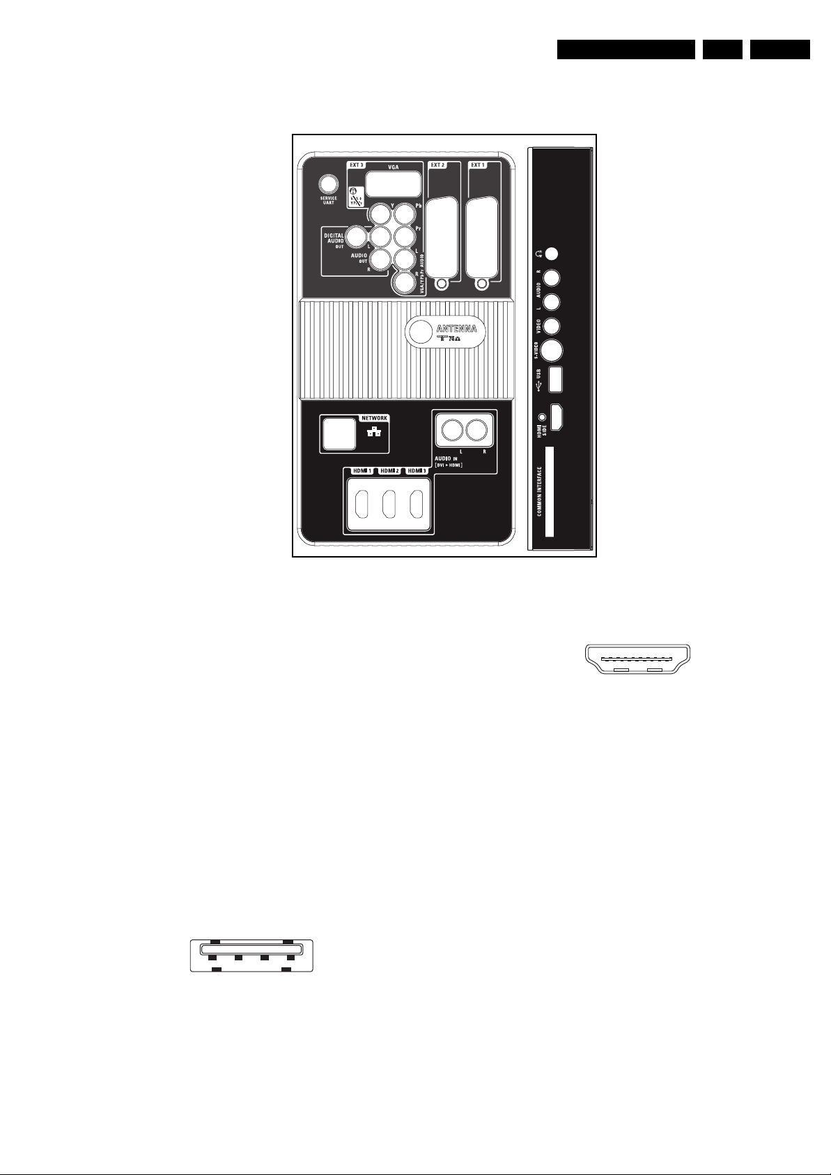
1.2 Connections
EN 3Q529.1E LA 1.
Note: The following connector colour abbreviations are used
(acc. to DIN/IEC 757): Bk= Black, Bu= Blue, Gn= Green,
Gy= Grey, Rd= Red, Wh= White, Ye= Yellow.
1.2.1 Side Connections
Headphone (Output)
Bk - Headphone 32 - 600 ohm / 10 mW ot
Cinch: Video CVBS - In, Audio - In
Rd - Audio R 0.5 V
Wh - Audio L 0.5 V
Ye - Video CVBS 1 V
/ 10 kohm jq
RMS
/ 10 kohm jq
RMS
/ 75 ohm jq
PP
S-Video (Hosiden): Video Y/C - In
1 - Ground Y Gnd H
2 - Ground C Gnd H
3 - Video Y 1 V
4 - Video C 0.3 V
/ 75 ohm j
PP
/ 75 ohm j
PP
USB2.0
1 2 3 4
E_06532_022.eps
300904
Figure 1-2 USB (type A)
1-+5V k
2 - Data (-) jk
3 - Data (+) jk
4 - Ground Gnd H
Figure 1-1 Connection overview
HDMI: Digital Video, Digital Audio - In
1 - D2+ Data channel j
2-Shield Gnd H
3 - D2- Data channel j
4 - D1+ Data channel j
5-Shield Gnd H
6 - D1- Data channel j
7 - D0+ Data channel j
8-Shield Gnd H
9 - D0- Data channel j
10 - CLK+ Data channel j
11 - Shield Gnd H
12 - CLK- Data channel j
13 - n.c.
14 - n.c.
15 - DDC_SCL DDC clock j
16 - DDC_SDA DDC data jk
17 - Ground Gnd H
18 - +5V j
19 - HPD Hot Plug Detect j
20 - Ground Gnd H
Common Interface
68p- See diagram B07A jk
I_17660_123.eps
140308
19
18 2
1
E_06532_017.eps
250505
Figure 1-3 HDMI (type A) connector
Page 4
EN 4 Q529.1E LA1.
Technical Specifications, Connections, and Chassis Overview
1.2.2 Rear Connections
Service Connector (UART)
1 - Ground Gnd H
2 - UART_TX Transmit k
3 - UART_RX Receive j
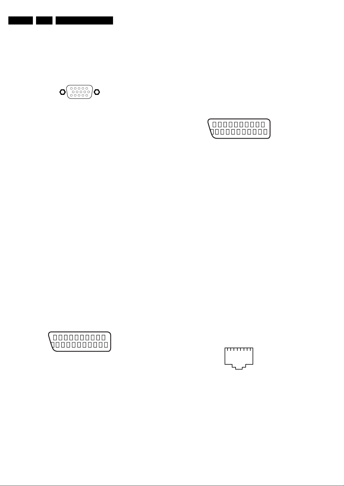
EXT 3 VGA: Video RGB - In
1
5
6
11
10
15
E_06532_002.eps
050404
Figure 1-4 VGA Connector
1 - Video Red 0.7 V
2 - Video Green 0.7 V
3 - Video Blue 0.7 V
/ 75 ohm j
PP
/ 75 ohm j
PP
/ 75 ohm j
PP
4-n.c.
5 - Ground Gnd H
6 - Ground Red Gnd H
7 - Ground Green Gnd H
8 - Ground Blue Gnd H
9-+5V
DC
+5 V j
10 - Ground Sync Gnd H
11 - n.c.
12 - DDC_SDA DDC data j
13 - H-sync 0 - 5 V j
14 - V-sync 0 - 5 V j
15 - DDC_SCL DDC clock j
EXT3: Cinch: S/PDIF - Out
Bk - Coaxial 0.4 - 0.6V
/ 75 ohm kq
PP
EXT3: Cinch: Video YPbPr - In
Gn - Video Y 1 V
Bu - Video Pb 0.7 V
Rd - Video Pr 0.7 V
/ 75 ohm jq
PP
/ 75 ohm jq
PP
/ 75 ohm jq
PP
EXT3: Cinch: Audio - Out
Rd - Audio - R 0.5 V
Wh - Audio - L 0.5 V
/ 10 kohm kq
RMS
/ 10 kohm kq
RMS
EXT3: Cinch: Audio - In
Rd - Audio - R 0.5 V
Wh - Audio - L 0.5 V
/ 10 kohm jq
RMS
/ 10 kohm jq
RMS
12 - n.c.
13 - Ground Red Gnd H
14 - Ground Data Gnd H
15 - Video Red 0.7 V
16 - Status/FBL 0 - 0.4 V: INT
/ 75 ohm j
PP
1 - 3 V: EXT / 75 ohm j
17 - Ground Video Gnd H
18 - Ground FBL Gnd H
19 - n.c.
20 - Video CVBS 1 V
21 - Shield Gnd H
/ 75 ohm j
PP
EXT2: Video RGB/YC - In, CVBS - In/Out, Audio - In/Out
21
20
E_06532_001.eps
2
1
050404
Figure 1-6 SCART connector
1 - Audio R 0.5 V
2 - Audio R 0.5 V
3 - Audio L 0.5 V
4 - Ground Audio Gnd H
/ 1 kohm k
RMS
/ 10 kohm j
RMS
/ 1 kohm k
RMS
5 - Ground Blue Gnd H
6 - Audio L 0.5 V
7 - Video Blue/C-out 0.7 V
/ 10 kohm j
RMS
/ 75 ohm jk
PP
8 - Function Select 0 - 2 V: INT
4.5 - 7 V: EXT 16:9
9.5 - 12 V: EXT 4:3 j
9 - Ground Green Gnd H
10 - Easylink P50 0 - 5 V / 4.7 kohm jk
11 - Video Green 0.7 V
/ 75 ohm j
PP
12 - n.c.
13 - Ground Red Gnd H
14 - Ground P50 Gnd H
15 - Video Red/C 0.7 V
16 - Status/FBL 0 - 0.4 V: INT
/ 75 ohm j
PP
1 - 3 V: EXT / 75 ohm j
17 - Ground Video Gnd H
18 - Ground FBL Gnd H
19 - Video CVBS 1 V
20 - Video CVBS/Y 1 V
21 - Shield Gnd H
/ 75 ohm k
PP
/ 75 ohm j
PP
EXT1: Video RGB/CVBS - In, Audio - In
21
20
E_06532_001.eps
2
1
050404
Figure 1-5 SCART connector
1-n.c.
2 - Audio R 0.5 V
3-n.c.
/ 10 kohm j
RMS
4 - Ground Audio Gnd H
5 - Ground Blue Gnd H
6 - Audio L 0.5 V
7 - Video Blue 0.7 V
/ 10 kohm j
RMS
/ 75 ohm j
PP
8 - Function Select 0 - 2 V: INT
4.5 - 7 V: EXT 16:9
9.5 - 12 V: EXT 4:3 j
9 - Ground Green Gnd H
10 - n.c.
11 - Video Green 0.7 V
/ 75 ohm j
PP
Aerial - In
- - IEC-type (EU) Coax, 75 ohm D
RJ45: Ethernet (if present)
112345678
E_06532_025.eps
210905
Figure 1-7 Ethernet connector
1 - TD+ Transmit signal k
2 - TD- Transmit signal k
3 - RD+ Receive signal j
4-n.c.
5-n.c.
6 - RD- Receive signal j
7-n.c.
8-n.c.
Page 5
Technical Specifications, Connections, and Chassis Overview
EN 5Q529.1E LA 1.
HDMI 1, 2 & 3 Digital Video, Digital Audio - In
19
18 2
Figure 1-8 HDMI (type A) connector
1 - D2+ Data channel j
2-Shield Gnd H
3 - D2- Data channel j
4 - D1+ Data channel j
5-Shield Gnd H
6 - D1- Data channel j
7 - D0+ Data channel j
8-Shield Gnd H
1
E_06532_017.eps
250505
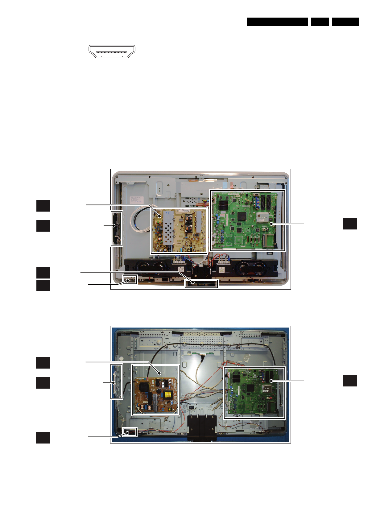
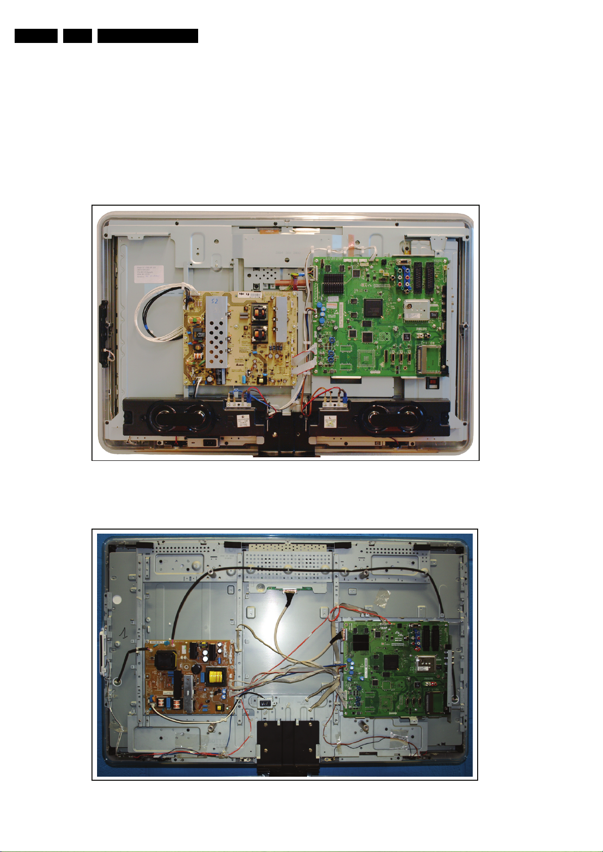
1.3 Chassis Overview
MAIN
A
SUPPLY PANEL
9 - D0- Data channel j
10 - CLK+ Data channel j
11 - Shield Gnd H
12 - CLK- Data channel j
13 - n.c.
14 - n.c.
15 - DDC_SCL DDC clock j
16 - DDC_SDA DDC data jk
17 - Ground Gnd H
18 - +5V j
19 - HPD Hot Plug Detect j
20 - Ground Gnd H
Cinch: Audio - In
Rd - Audio - R 0.5 V
Wh - Audio - L 0.5 V
/ 10 kohm jq
RMS
/ 10 kohm jq
RMS
KEYBOARD CONTROL
E
PANEL
LIGHTGUIDE
L
IR & LED PANEL
J
MAIN
A
SUPPLY PANEL
KEYBOARD CONTROL
E
PANEL
Figure 1-9 PWB/CBA locations 9-series
SMALL SIGNAL
BOARD
I_17660_104.eps
SMALL SIGNAL
BOARD
B
130308
B
IR & LED PANEL
J
Figure 1-10 PWB/CBA locations 7-series
I_17661_021.eps
180408
Page 6

EN 6 Q529.1E LA2.
Safety Instructions, Warnings, and Notes
2. Safety Instructions, Warnings, and Notes
Index of this chapter:
2.1 Safety Instructions
2.2 Warnings
2.3 Notes
2.1 Safety Instructions
Safety regulations require the following during a repair:
• Connect the set to the Mains/AC Power via an isolation
transformer (> 800 VA).
• Replace safety components, indicated by the symbol h,
only by components identical to the original ones. Any
other component substitution (other than original type) may
increase risk of fire or electrical shock hazard.
Safety regulations require that after a repair, the set must be
returned in its original condition. Pay in particular attention to
the following points:
• Route the wire trees correctly and fix them with the
mounted cable clamps.
• Check the insulation of the Mains/AC Power lead for
external damage.
• Check the strain relief of the Mains/AC Power cord for
proper function.
• Check the electrical DC resistance between the Mains/AC
Power plug and the secondary side (only for sets that have
a Mains/AC Power isolated power supply):
1. Unplug the Mains/AC Power cord and connect a wire
between the two pins of the Mains/AC Power plug.
2. Set the Mains/AC Power switch to the “on” position
(keep the Mains/AC Power cord unplugged!).
3. Measure the resistance value between the pins of the
Mains/AC Power plug and the metal shielding of the
tuner or the aerial connection on the set. The reading
should be between 4.5 Mohm and 12 Mohm.
4. Switch “off” the set, and remove the wire between the
two pins of the Mains/AC Power plug.
• Check the cabinet for defects, to prevent touching of any
inner parts by the customer.
2.2 Warnings
• All ICs and many other semiconductors are susceptible to
electrostatic discharges (ESD w). Careless handling
during repair can reduce life drastically. Make sure that,
during repair, you are connected with the same potential as
the mass of the set by a wristband with resistance. Keep
components and tools also at this same potential.
• Be careful during measurements in the high voltage
section.
• Never replace modules or other components while the unit
is switched “on”.
• When you align the set, use plastic rather than metal tools.
This will prevent any short circuits and the danger of a
circuit becoming unstable.
2.3 Notes
2.3.1 General
• Measure the voltages and waveforms with regard to the
chassis (= tuner) ground (H), or hot ground (I), depending
on the tested area of circuitry. The voltages and waveforms
shown in the diagrams are indicative. Measure them in the
Service Default Mode (see chapter 5) with a colour bar
signal and stereo sound (L: 3 kHz, R: 1 kHz unless stated
otherwise) and picture carrier at 475.25 MHz for PAL, or
61.25 MHz for NTSC (channel 3).
• Where necessary, measure the waveforms and voltages
with (D) and without (E) aerial signal. Measure the
voltages in the power supply section both in normal
operation (G) and in stand-by (F). These values are
indicated by means of the appropriate symbols.
• Manufactured under license from Dolby Laboratories.
“Dolby”, “Pro Logic”, “Virtual Dolby Digital” and the “doubleD symbol”, are trademarks of Dolby Laboratories.
2.3.2 Schematic Notes
• All resistor values are in ohms, and the value multiplier is
often used to indicate the decimal point location (e.g. 2K2
indicates 2.2 kohm).
• Resistor values with no multiplier may be indicated with
either an “E” or an “R” (e.g. 220E or 220R indicates 220
ohm).
• All capacitor values are given in micro-farads (μ = × 10
nano-farads (n = × 10
• Capacitor values may also use the value multiplier as the
decimal point indication (e.g. 2p2 indicates 2.2 pF).
• An “asterisk” (*) indicates component usage varies. Refer
to the diversity tables for the correct values.
• The correct component values are listed in the Spare Parts
List. Therefore, always check this list when there is any
doubt.
2.3.3 BGA (Ball Grid Array) ICs
Introduction
For more information on how to handle BGA devices, visit this
URL: www.atyourservice.ce.philips.com (needs subscription,
not available for all regions). After login, select “Magazine”,
then go to “Repair downloads”. Here you will find Information
on how to deal with BGA-ICs.
BGA Temperature Profiles
For BGA-ICs, you must use the correct temperature-profile,
which is coupled to the 12NC. For an overview of these profiles,
visit the website www.atyourservice.ce.philips.com (needs
subscription, but is not available for all regions)
You will find this and more technical information within the
“Magazine”, chapter “Repair downloads”.
For additional questions please contact your local repair help
desk.
2.3.4 Lead-free Soldering
Due to lead-free technology some rules have to be respected
by the workshop during a repair:
• Use only lead-free soldering tin Philips SAC305 with order
code 0622 149 00106. If lead-free solder paste is required,
please contact the manufacturer of your soldering
equipment. In general, use of solder paste within
workshops should be avoided because paste is not easy to
store and to handle.
• Use only adequate solder tools applicable for lead-free
soldering tin. The solder tool must be able:
– To reach a solder-tip temperature of at least 400°C.
– To stabilize the adjusted temperature at the solder-tip.
– To exchange solder-tips for different applications.
• Adjust your solder tool so that a temperature of around
360°C - 380°C is reached and stabilized at the solder joint.
Heating time of the solder-joint should not exceed ~ 4 sec.
Avoid temperatures above 400°C, otherwise wear-out of
tips will increase drastically and flux-fluid will be destroyed.
To avoid wear-out of tips, switch “off” unused equipment or
reduce heat.
• Mix of lead-free soldering tin/parts with leaded soldering
tin/parts is possible but PHILIPS recommends strongly to
-9
), or pico-farads (p = × 10
-12
-6
),
).
Page 7
avoid mixed regimes. If this cannot be avoided, carefully
clear the solder-joint from old tin and re-solder with new tin.
2.3.5 Alternative BOM identification
The third digit in the serial number (example:
AG2B0335000001) indicates the number of the alternative
B.O.M. (Bill Of Materials) that has been used for producing the
specific TV set. In general, it is possible that the same TV
model on the market is produced with e.g. two different types
of displays, coming from two different suppliers. This will then
result in sets which have the same CTN (Commercial Type
Number; e.g. 28PW9515/12) but which have a different B.O.M.
number.
By looking at the third digit of the serial number, one can
identify which B.O.M. is used for the TV set he is working with.
If the third digit of the serial number contains the number “1”
(example: AG1B033500001), then the TV set has been
manufactured according to B.O.M. number 1. If the third digit is
a “2” (example: AG2B0335000001), then the set has been
produced according to B.O.M. no. 2. This is important for
ordering the correct spare parts!
For the third digit, the numbers 1...9 and the characters A...Z
can be used, so in total: 9 plus 26= 35 different B.O.M.s can be
indicated by the third digit of the serial number.
Identification: The bottom line of a type plate gives a 14-digit
serial number. Digits 1 and 2 refer to the production centre (e.g.
AG is Bruges), digit 3 refers to the B.O.M. code, digit 4 refers
to the Service version change code, digits 5 and 6 refer to the
production year, and digits 7 and 8 refer to production week (in
example below it is 2006 week 17). The 6 last digits contain the
serial number.
Directions for Use
MODEL :
PROD.NO:
32PF9968/10
AG 1A0617 000001
220-240V 50/60Hz
VHF+S+H+UHF
S
Figure 2-1 Serial number (example)
2.3.6 Board Level Repair (BLR) or Component Level Repair
(CLR)
If a board is defective, consult your repair procedure to decide
if the board has to be exchanged or if it should be repaired on
component level.
If your repair procedure says the board should be exchanged
completely, do not solder on the defective board. Otherwise, it
cannot be returned to the O.E.M. supplier for back charging!
2.3.7 Practical Service Precautions
• It makes sense to avoid exposure to electrical shock.
While some sources are expected to have a possible
dangerous impact, others of quite high potential are of
limited current and are sometimes held in less regard.
• Always respect voltages. While some may not be
dangerous in themselves, they can cause unexpected
reactions that are best avoided. Before reaching into a
powered TV set, it is best to test the high voltage insulation.
It is easy to do, and is a good service precaution.
EN 7Q529.1E LA 3.
MADE IN BELGIUM
~
128W
BJ3.0E LA
E_06532_024.eps
260308
3. Directions for Use
You can download this information from the following websites:
http://www.philips.com/support
http://www.p4c.philips.com
Page 8
EN 8 Q529.1E LA4.
Mechanical Instructions
4. Mechanical Instructions
Index of this chapter:
4.1 Cable Dressing
4.2 Service Positions
4.3 Assy/Panel Removal VE8 Styling
4.4 Assy/Panel Removal ME8+ Styling
4.5 Set Re-assembly.
4.1 Cable Dressing
Notes:
• Figures below can deviate slightly from the actual situation,
due to the different set executions.
Figure 4-1 Cable dressing 9-series
I_17660_105.eps
130308
Figure 4-2 Cable dressing 7-series
I_17661_022.eps
180408
Page 9
4.2 Service Positions
For easy servicing of this set, there are a few possibilities
created:
• The buffers from the packaging (see figure “Rear cover”).
• Foam bars (created for Service).
4.2.1 Foam Bars
1
Required for sets
1
42"
E_06532_018.eps
171106
Figure 4-3 Foam bars
Mechanical Instructions
EN 9Q529.1E LA 4.
The foam bars (order code 3122 785 90580 for two pieces) can
be used for all types and sizes of Flat TVs. See figure “Foam
bars” for details. Sets with a display of 42" and larger, require
four foam bars [1]. Ensure that the foam bars are always
supporting the cabinet and never only the display.
Caution: Failure to follow these guidelines can seriously
damage the display!
By laying the TV face down on the (ESD protective) foam bars,
a stable situation is created to perform measurements and
alignments. By placing a mirror under the TV, the screen can
be monitored.
Page 10
EN 10 Q529.1E LA4.
Mechanical Instructions
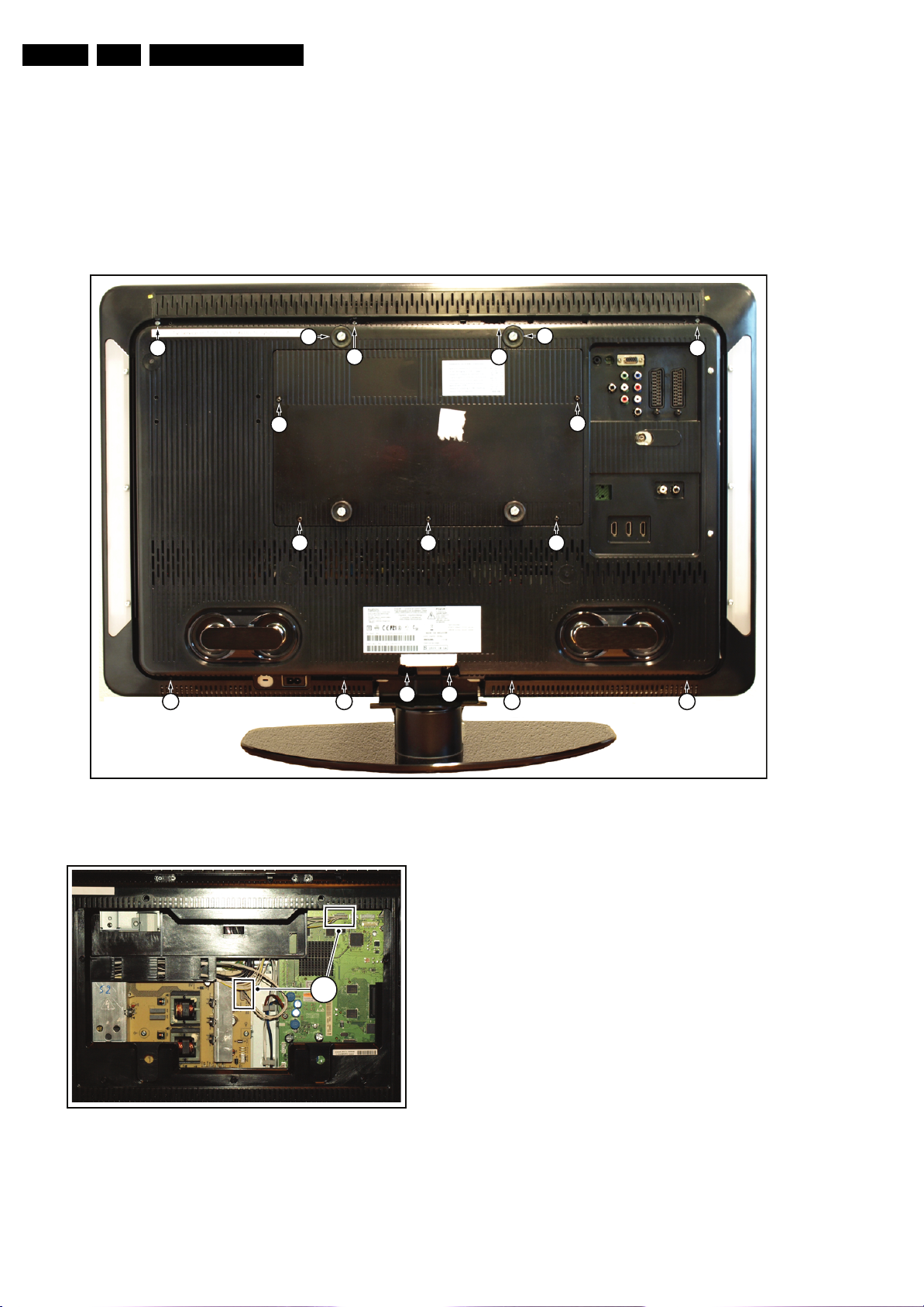
4.3 Assy/Panel Removal VE8 Styling
4.3.1 Rear Cover
Warning: Disconnect the mains power cord before removing
the rear cover.
Note: It is necessity to release the fixation screws from the
stand before removing the rear cover.
Refer to next figures for details.
5
2
1
5 5
1. Remove the mushrooms [1].
2. Remove the fixation screws [2] from the hatch and lift the
hatch from the rear cover.
3. Unplug the connectors [3].
4. Remove the fixation screws from the stand. Please note
that the set is now mechanically not secured and may be
unstable.
5. Remove the fixation screws [5] that secure the rear cover.
6. Lift the rear cover from the TV. Make sure that wires and
flat foils are not damaged while lifting the rear cover from
the set.
1
5
2
222
5
4 4
555
I_17660_106.eps
130308
Figure 4-4 Rear Cover
3
Figure 4-5 Hatch
I_17660_107.eps
130308
Page 11
Mechanical Instructions
EN 11Q529.1E LA 4.
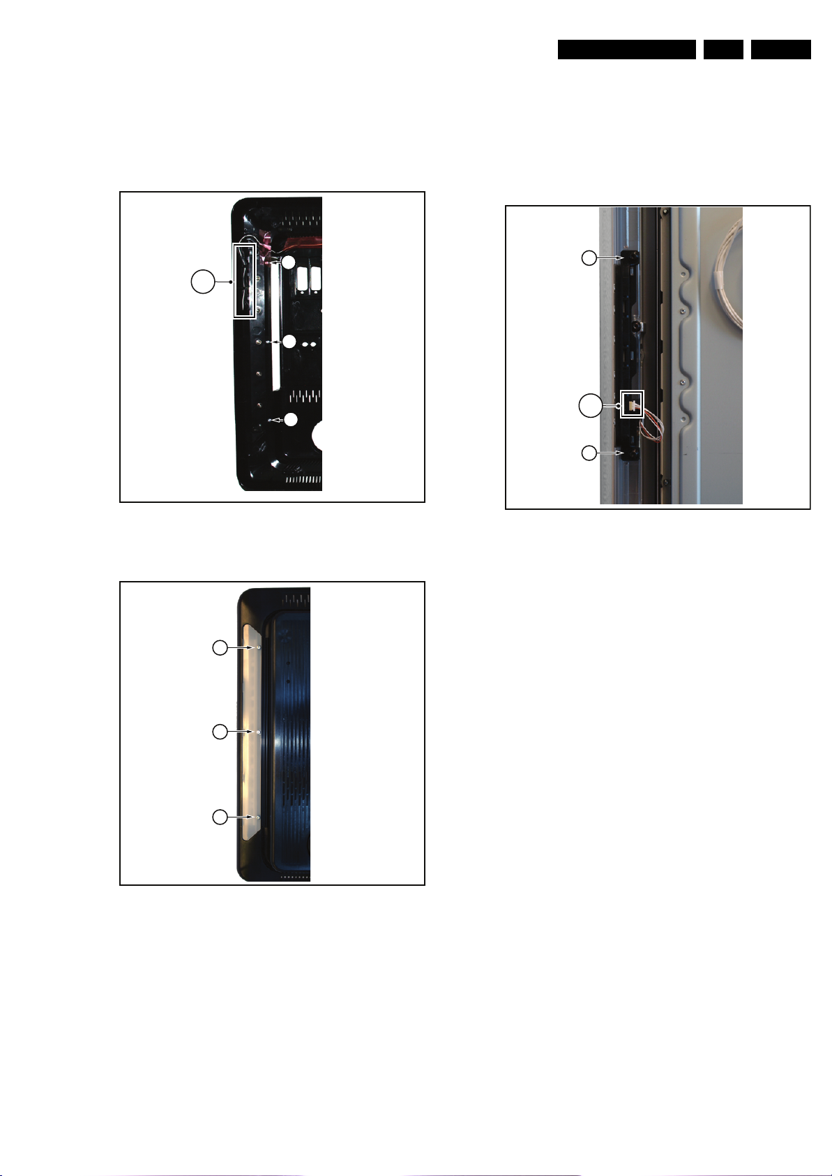
4.3.2 Ambilight
Refer to next figure for details.
1. Release the wire from the wire guides [1].
2. Remove the fixation screws [2].
3. Remove the cover screws [3] and take out the whole unit.
When defective, replace the whole unit.
2
1
2
2
4.3.3 Key Board
Refer to next figure for details.
1. Unplug the key board connector [1] from the IR & LED
board.
2. Remove the screws [2].
3. Lift the unit and take it out of the set.
When defective, replace the whole unit.
2
1
2
Figure 4-6 Ambilight inside cover
3
3
3
I_17660_108.eps
130308
I_17660_109.eps
130308
Figure 4-8 Key Board
I_17660_110.eps
130308
Figure 4-7 Ambilight outside cover
Page 12
EN 12 Q529.1E LA4.
Mechanical Instructions
4.3.4 Bass-midrange Speakers
Refer to next figure for details.
1. Release the speaker connectors [1] from unit.
2. Remove the screw [1] and lift the whole unit from the set.
Take the speakers out together with their casing. When
defective, replace the whole unit.
2
Figure 4-9 Bass-midrange Speaker
1
I_17660_111.eps
130308
4.3.6 Display Supply Panel
Refer to next figure for details.
1. Unplug the connectors [1].
2. Remove the fixation screws [2].
3. Take the board out.
2
1
2
1
2
Figure 4-11 Display Supply Panel
2
2
2
(
2x)
2
2
I_17660_113.eps
130308
4.3.5 Tweeters
Refer to next figure for details.
1. Remove the bass-midrange speaker as described earlier.
2. Remove the screw [1] and lift the whole unit from the set.
When defective, replace the whole unit.
1
Figure 4-10 Tweeters
I_17660_112.eps
130308
4.3.7 Small Signal Board (SSB)
Refer to next figure for details.
Caution: it is mandatory to remount all different screws at their
original position during re-assembly. Failure to do so may result
in damaging the SSB.
Refer to next figures or details.
1. Unplug the LVDS connector [1].
Caution: be careful, as this is a very fragile connector!
2. Unplug the connectors [2].
3. Remove the screw [3] from the side I/O cover.
4. Remove the fixation screws [4].
5. The SSB can now be taken out of the set.
4
1
4
2
2
4
2
(2x)
4
4
4
3
4
Figure 4-12 Small Signal Board
I_17660_114.eps
130308
Page 13
4.3.8 LCD Panel
Refer to next figure for details.
1. Remove the SSB as described earlier.
2. Remove the Bass-midrange speakers as described earlier.
3. Remove the Tweeters as described earlier.
4. Unplug the connectors [1].
5. Remove the fixation screws [2].
6. Remove the fixation screws [3].
7. Lift out the sub frame.
8. The LCD panel can now be lifted from the front cabinet.
When defective, replace the whole unit.
Mechanical Instructions
1
EN 13Q529.1E LA 4.
2
3x
)
(
1
2
I_17660_117.eps
130308
2
2
3
2
1
2x
)
(
3
3
2
2
2
Figure 4-13 LCD Panel
4.3.9 Rim
Refer to next figure for details.
1. Do all steps as described in the removal of the LCD panel
except the last step.
2. Remove the screws [1].
1
2
3
22
I_17660_115.eps
2
2
130308
Figure 4-15 IR & LED Board
4.3.11 Lightguide
Refer to next figure for details.
1. Do all steps as described in the removal of the Rim.
2. Release the cables from the cable clamps [1].
3. Remove screws [2] and lift the lightguide from the front
cover.
4. Release the board by pushing up the clamps in the
direction of the arrows.
5. Remove the unit from the front cover.
When defective, replace the whole unit.
1
3 3
2 2
Figure 4-16 IR & LED Board
4.4 Assy/Panel Removal ME8+ Styling
I_17660_118.eps
140308
1
Figure 4-14 Rim
4.3.10 IR & LED Board
Refer to next figure for details.
1. Do all steps as described in the removal of the Rim.
2. Remove screws [1] and lift the IR & LED Board from the
front cover.
3. Lift the board and take it out of the set.
4. Release the cables from the cable clamps.
5. Unplug the connectors [3].
When defective, replace the whole unit.
1
I_17660_116.eps
130308
Refer to the Q528.2E LA Service Manual.
4.5 Set Re-assembly
To re-assemble the whole set, execute all processes in reverse
order.
Notes:
• While re-assembling, make sure that all cables are placed
and connected in their original position. See figure “Cable
dressing”.
• Pay special attention not to damage the EMC foams on the
SSB shields. Ensure that EMC foams are mounted
correctly.
Page 14
EN 14 Q529.1E LA5.
Service Modes, Error Codes, and Fault Finding
5. Service Modes, Error Codes, and Fault Finding
Index of this chapter:
5.1 Test Points
5.2 Service Modes
5.3 Stepwise Start-up
5.4 Service Tools
5.5 Error Codes
5.6 The Blinking LED Procedure
5.7 Protections
5.8 Fault Finding and Repair Tips
5.9 Software Upgrading
5.1 Test Points
As most signals are digital, it will be difficult to measure
waveforms with a standard oscilloscope. However, several key
ICs are capable of generating test patterns, which can be
controlled via ComPair. In this way it is possible to determine
which part is defective.
Perform measurements under the following conditions:
• Service Default Mode.
• Video: Colour bar signal.
• Audio: 3 kHz left, 1 kHz right.
5.2 Service Modes
Service Default mode (SDM) and Service Alignment Mode
(SAM) offers several features for the service technician, while
the Customer Service Mode (CSM) is used for communication
between the call centre and the customer.
This chassis also offers the option of using ComPair, a
hardware interface between a computer and the TV chassis. It
offers the abilities of structured troubleshooting, error code
reading, and software version read-out for all chassis.
(see also section “5.4.1 ComPair”).
5.2.1 Service Default Mode (SDM)
– Skip/blank of non-favourite pre-sets.
How to Activate SDM
For this chassis there are two kinds of SDM: an analog SDM
and a digital SDM. Tuning will happen according table “SDM
Default Settings”.
• Analog SDM: use the standard RC-transmitter and key in
the code “062596”, directly followed by the “MENU” button.
Note: It is possible that, together with the SDM, the main
menu will appear. To switch it “off”, push the “MENU”
button again.
• Digital SDM: use the standard RC-transmitter and key in
the code “062593”, directly followed by the “MENU” button.
Note: It is possible that, together with the SDM, the main
menu will appear. To switch it “off”, push the “MENU”
button again.
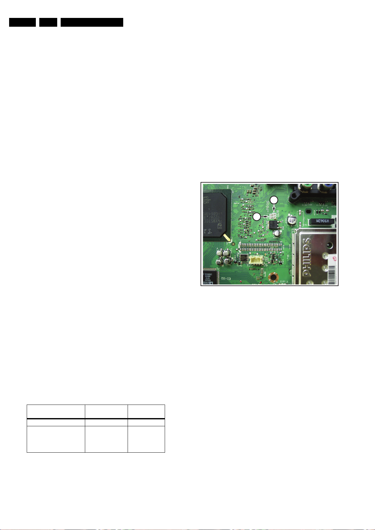
• Analog SDM can also be activated by shorting for a
moment the two solder pads (see figure “Service mode
pads”) on the SSB, with the indication “SDM”.
1
2
H_16770_100.eps
130707
Figure 5-1 Service mode pads
Purpose
• To create a pre-defined setting, to get the same
measurement results as given in this manual.
• To override SW protections detected by stand-by
processor and make the TV start up to the step just before
protection (a sort of automatic stepwise start up). See
section “5.3 Stepwise Start-up”.
• To start the blinking LED procedure where only layer 2
errors are displayed. (see also section “5.5 Error Codes”)
Specifications
Table 5-1 SDM default settings
Default
Region Freq. (MHz)
Europe, AP(PAL/Multi) 475.25 PAL B/G
Europe, AP DVB-T 546.00 PID
Video: 0B 06 PID
PCR: 0B 06 PID
Audio: 0B 07
• All picture settings at 50% (brightness, colour, contrast).
• All sound settings at 50%, except volume at 25%.
• All service-unfriendly modes (if present) are disabled, like:
– (Sleep) timer.
– Child/parental lock.
– Picture mute (blue mute or black mute).
– Automatic volume levelling (AVL).
system
DVB-T
After activating this mode, “SDM” will appear in the upper right
corner of the screen (when a picture is available).
How to Navigate
When the “MENU” button is pressed on the RC transmitter, the
set will toggle between the SDM and the normal user menu
(with the SDM mode still active in the background).
How to Exit SDM
Use one of the following methods:
• Switch the set to STAND-BY via the RC-transmitter.
• Via a standard customer RC-transmitter: key in “00”sequence.
5.2.2 Service Alignment Mode (SAM)
Purpose
• To perform (software) alignments.
• To change option settings.
• To easily identify the used software version.
• To view operation hours.
• To display (or clear) the error code buffer.
How to Activate SAM
Via a standard RC transmitter: key in the code “062596”
directly followed by the “INFO” button. After activating SAM
with this method a service warning will appear on the screen,
continue by pressing the red button on the RC.
Page 15
Service Modes, Error Codes, and Fault Finding
Contents of SAM:
• Hardware Info.
– A. SW Version. Displays the software version of the
main software (example: Q591E-1.2.3.4 =
AAAAB_X.Y.W.Z).
• AAAA= the chassis name.
• B= the region: A= AP, E= EU, L= LatAm, U = US.
For AP sets it is possible that the Europe software
version is used.
• X.Y.W.Z= the software version, where X is the
main version number (different numbers are not
compatible with one another) and Y.W.Z is the sub
version number (a higher number is always
compatible with a lower number).
– B. SBY PROC Version. Displays the software version
of the stand-by processor.
– C. Production Code. Displays the production code of
the TV, this is the serial number as printed on the back
of the TV set. Note that if an NVM is replaced or is
initialized after corruption, this production code has to
be re-written to NVM. ComPair will foresee in a
possibility to do this.
• Operation Hours. Displays the accumulated total of
operation hours (not the stand-by hours). Every time the
TV is switched “on/off”, 0.5 hours is added to this number.
• Errors (followed by maximum 10 errors). The most recent
error is displayed at the upper left (for an error explanation
see section “5.5 Error Codes”).
• Reset Error Buffer. When “cursor right” (or the “OK
button) is pressed and then the “OK” button is pressed, the
error buffer is reset.
• Alignments. This will activate the “ALIGNMENTS” submenu.
• Dealer Options. Extra features for the dealers.
• Options. Extra features for Service. For more info
regarding option codes, see chapter 8 “Alignments”.
Note that if the option code numbers are changed, these
have to be confirmed with pressing the “OK” button before
the options are stored. Otherwise changes will be lost.
• Initialize NVM. The moment the processor recognizes a
corrupted NVM, the “initialize NVM” line will be highlighted.
Now, two things can be done (dependent of the service
instructions at that moment):
– Save the content of the NVM via ComPair for
development analysis, before initializing. This will give
the Service department an extra possibility for
diagnosis (e.g. when Development asks for this).
– Initialize the NVM.
Note: When the NVM is corrupted, or replaced, there is a high
possibility that no picture appears because the display code is
not correct. So, before initializing the NVM via the SAM, a
picture is necessary and therefore the correct display option
has to be entered. Refer to chapter 8 “Alignments” for details.
To adapt this option, it’s advised to use ComPair (the correct
HEX values for the options can be found in chapter 8
“Alignments”) or a method via a standard RC (described
below).
Changing the display option via a standard RC: Key in the
code “062598” directly followed by the “MENU” button and
“XXX” (where XXX is the 3 digit decimal display code as
mentioned in table “Option code overview” in chapter 8
“Alignments”). Make sure to key in all three digits, also the
leading zero’s. If the above action is successful, the front LED
will go out as an indication that the RC sequence was correct.
After the display option is changed in the NVM, the TV will go
to the Stand-by mode. If the NVM was corrupted or empty
before this action, it will be initialized first (loaded with default
values). This initializing can take up to 20 seconds.
EN 15Q529.1E LA 5.
Display Option
Code
39mm
040
PHILIPS
MODEL:
32PF9968/10
27mm
PROD.SERIAL NO:
AG 1A0620 000001
(CTN Sticker)
E_06532_038.eps
240108
Figure 5-2 Location of Display Option Code sticker
• Store - go right. All options and alignments are stored
when pressing “cursor right” (or the “OK” button) and then
the “OK”-button.
• SW Maintenance.
– SW Events. Not useful for Service purposes. In case
of specific software problems, the development
department can ask for this info.
– HW Events. Not useful for Service purposes. In case
of specific software problems, the development
department can ask for this info.
• Test settings. For development purposes only.
• Upload to USB. To upload several settings from the TV to
an USB stick, which is connected to the SSB. The items are
“Channel list”, “Personal settings”, “Option codes”,
“Display-related alignments” and “History list”. First a
directory “repair\” has to be created in the root of the USB
stick. To upload the settings select each item separately,
press “cursor right” (or the “OK button), confirm with “OK”
and wait until “Done” appears. In case the download to the
USB stick was not successful “Failure” will appear. In this
case, check if the USB stick is connected properly and if
the directory “repair” is present in the root of the USB stick.
Now the settings are stored onto the USB stick and can be
used to download onto another TV or other SSB.
Uploading is of course only possible if the software is
running and if a picture is available. This method is created
to be able to save the customer’s TV settings and to store
them into another SSB.
• Download to USB. To download several settings from the
USB stick to the TV. Same way of working as with
uploading. To make sure that the download of the channel
list from USB to the TV is executed properly, it is necessary
to restart the TV and tune to a valid preset if necessary.
Note: The “History list item” can not be downloaded from
USB to the TV. This is a “read-only” item. In case of
specific problems, the development department can ask
for this info.
• Development file versions. Not useful for Service
purposes, this information is only used by the development
department.
How to Navigate
• In SAM, the menu items can be selected with the
“CURSOR UP/DOWN” key (or the scroll wheel) on the RCtransmitter. The selected item will be highlighted. When not
all menu items fit on the screen, move the “CURSOR UP/
DOWN” key to display the next/previous menu items.
• With the “CURSOR LEFT/RIGHT” keys (or the scroll
wheel), it is possible to:
– (De) activate the selected menu item.
– (De) activate the selected sub menu.
• With the “OK” key, it is possible to activate the selected
action.
How to Exit SAM
Use one of the following methods:
• Press the “MENU” button on the RC-transmitter.
Page 16

EN 16 Q529.1E LA5.
Service Modes, Error Codes, and Fault Finding
• Switch the set to STAND-BY via the RC-transmitter.
5.2.3 Customer Service Mode (CSM)
Purpose
When a customer is having problems with his TV-set, he can
call his dealer or the Customer Helpdesk. The service
technician can then ask the customer to activate the CSM, in
order to identify the status of the set. Now, the service
technician can judge the severity of the complaint. In many
cases, he can advise the customer how to solve the problem,
or he can decide if it is necessary to visit the customer.
The CSM is a read only mode; therefore, modifications in this
mode are not possible.
When in this chassis CSM is activated, a testpattern will be
displayed during 5 seconds (1 second Blue, 1 second Green
and 1 second Red, then again 1 second Blue and 1 second
Green). This test pattern is generated by the PNX5100. So if
this test pattern is shown, it could be determined that the back
end video chain (PNX5100, LVDS, and display) of the SSB is
working.
To determine if the MPEG4-circuit is working (in case of an
MPEG4-set), push the “MUTE” button during CSM to display
another test pattern. This is a forced input selection to make
sure the test pattern is visible. If this test pattern is not shown,
it is possible that the settings are not correct (for instance in
SAM the MPEG4-option is “NOT PRESENT”). The display of
this test pattern is a toggle function, pressing the “MUTE” key
again removes this test pattern.
When CSM is activated and there is a USB stick connected to
the TV, the software will dump the complete CSM content to the
USB stick. The file (Csm.txt) will be saved in the root of the USB
stick. This info can be handy if no information is displayed.
Also when CSM is activated, the layer 1 error is displayed via
blinking LED. Only the latest error is displayed. (see also
section “5.5 Error Codes”).
How to Activate CSM
Key in the code “123654” via the standard RC transmitter.
Note: Activation of the CSM is only possible if there is no (user)
menu on the screen!
How to Navigate
By means of the “CURSOR-DOWN/UP” knob (or the scroll
wheel) on the RC-transmitter, can be navigated through the
menus.
Contents of CSM
The contents are reduced to 3 pages: General, Software
versions and Quality items. The group names itself are not
shown anywhere in the CSM menu.
• 12NC SSB. Gives an identification of the SSB as stored in
NVM. Note that if an NVM is replaced or is initialized after
corruption, this identification number has to be re-written to
NVM. ComPair will foresee in a possibility to do this. This
identification number is the 12nc number of the SSB.
• 12NC display. Shows the 12NC of the display
• 12NC supply. Shows the 12NC of the supply.
• 12NC “bolt-on”.
module.
Software versions
• Current main SW. Displays the built-in main software
version. In case of field problems related to software,
software can be upgraded. As this software is consumer
upgradeable, it will also be published on the Internet.
Example: Q591E_1.2.3.4
• Standby SW. Displays the built-in stand-by processor
software version. Upgrading this software will be possible
via ComPair or via USB (see chapter Software upgrade).
Example: STDBY_3.0.1.2.
• MOP ambient light SW. Displays the MOP ambient light
EPLD SW.
• MPEG4 software. Displays the MPEG4 software (optional
for sets with MPEG4).
• PNX5100 boot NVM. Displays the SW-version that is used
in the PNX5100 boot NVM.
Quality items
• Signal quality. Poor / average /good
• Child lock. Not active / active. This is a combined item for
locks. If any lock (Preset lock, child lock, lock after or
parental lock) is active, the item shall show “active”.
• Table channel changed. This item is for development
purpose, it will be defined later.
• Key missing. This is a combined item for keys. The keys
have a separate bit and the sum is displayed in decimal
value.
– HDMI key valid = 001
– MAC key valid = 010
Important remark here : due to a software bug, the
MAC key is missing and not valid when “2” is displayed
in CSM.So, if for instance the HDMI and MAC keys are
both valid, the decimal value in CSM “1” is displayed
and not “3”.
– BDS key valid = 100
If 3 keys are valid the value: “5” is displayed(should be
“7” but due to the software bug).
• CI slot present. If the common interface module is
detected the result will be “YES”, else “NO”.
• HDMI input format. The detected input format of the
HDMI.
• HDMI audio input stream. The HDMI audio input stream
is displayed: present / not present.
• HDMI video input stream. The HDMI video input stream
is displayed: present / not present.
Shows the 12NC of the “BOLT-ON”-
General
• Set Type. This information is very helpful for a helpdesk/
workshop as reference for further diagnosis. In this way, it
is not necessary for the customer to look at the rear of the
TV-set. Note that if an NVM is replaced or is initialized after
corruption, this set type has to be re-written to NVM.
ComPair will foresee in a possibility to do this.
• Production Code. Displays the production code (the serial
number) of the TV. Note that if an NVM is replaced or is
initialized after corruption, this production code has to be
re-written to NVM. ComPair will foresee a in possibility to
do this.
• Installed date. Indicates the date of the first installation of
the TV. This date is acquired via time extraction.
• Options 1. Gives the option codes of option group 1 as set
in SAM (Service Alignment Mode).
• Options 2. Gives the option codes of option group 2 as set
in SAM (Service Alignment Mode).
How to Exit CSM
Press “MENU” on the RC-transmitter.
Page 17
Service Modes, Error Codes, and Fault Finding
EN 17Q529.1E LA 5.
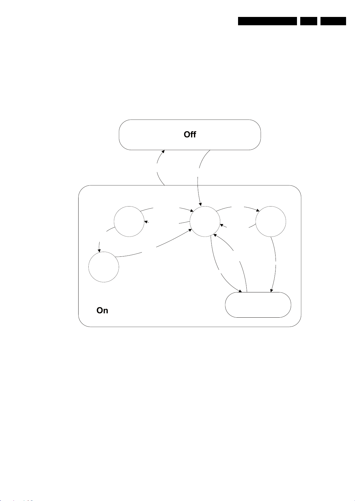
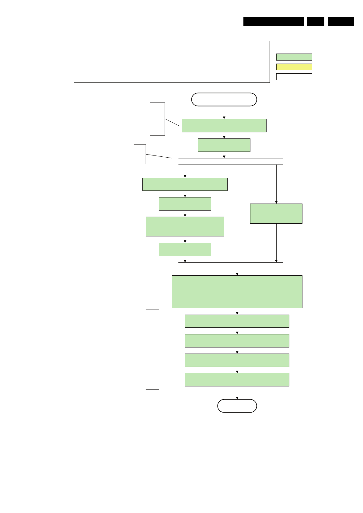
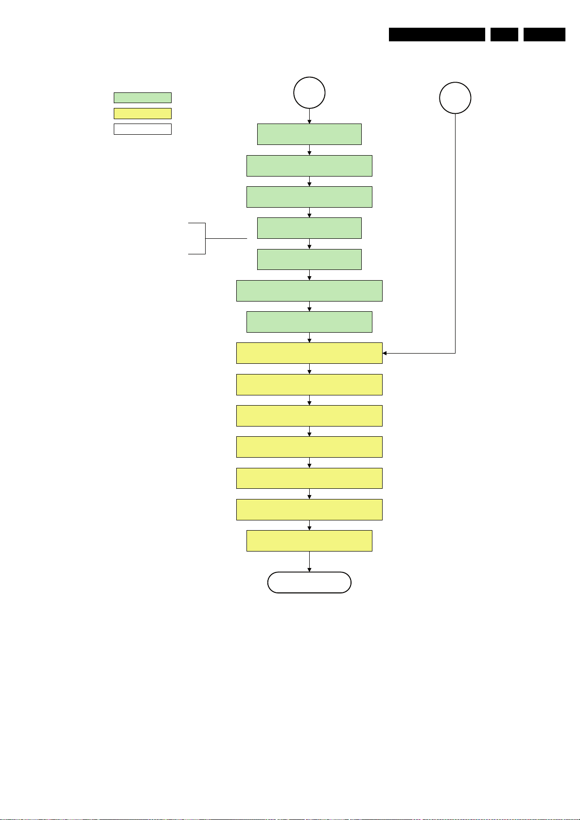
5.3 Stepwise Start-up
When the TV is in a protection state due to an error detected by
stand-by software (error blinking is displayed) and SDM is
activated via shortcutting the pins on the SSB, the TV starts up
until it reaches the situation just before protection. So, this is a
kind of automatic stepwise start-up. In combination with the
start-up diagrams below, you can see which supplies are
present at a certain moment. Important to know is, that if e.g.
the 3V3 detection fails and thus error layer 2 = 18 is blinking
while the TV is restarted via SDM, the Stand-by Processor will
enable the 3V3, but the TV set will not go to protection now.
The TV will stay in this situation until it is reset (Mains/AC
Power supply interrupted). Caution: in case the start up in this
St by
-Tact switch Pushed
-last status is hibernate
after mains ON
Tact switch
Hibernate
Mains
off
-WakeUp requested
-Acquisition needed
-No data Acquisition
required
-tact SW pushed
-last status is hibernate
after mains ON
pushed
Mains
on
Semi
St by
mode with a faulty FET 7U08 is done, you can destroy all IC’s
supplied by the +3V3, due to overvoltage (12V on 3V3-line). It
is recommended to measure first the FET 7U08 or others
FET’s on shortcircuit before activating SDM via the service
pads.
The abbreviations “SP” and “MP” in the figures stand for:
• SP: protection or error detected by the Stand-by
Processor.
• MP: protection or error detected by the MIPS Main
Processor.
WakeUp
requested
Active
- St by requested
-tact SW pushed
WakeUp
requested
(SDM)
GoToProtection
GoToProtection
Figure 5-3 Transition diagram
Protection
I_17660_124.eps
140308
Page 18
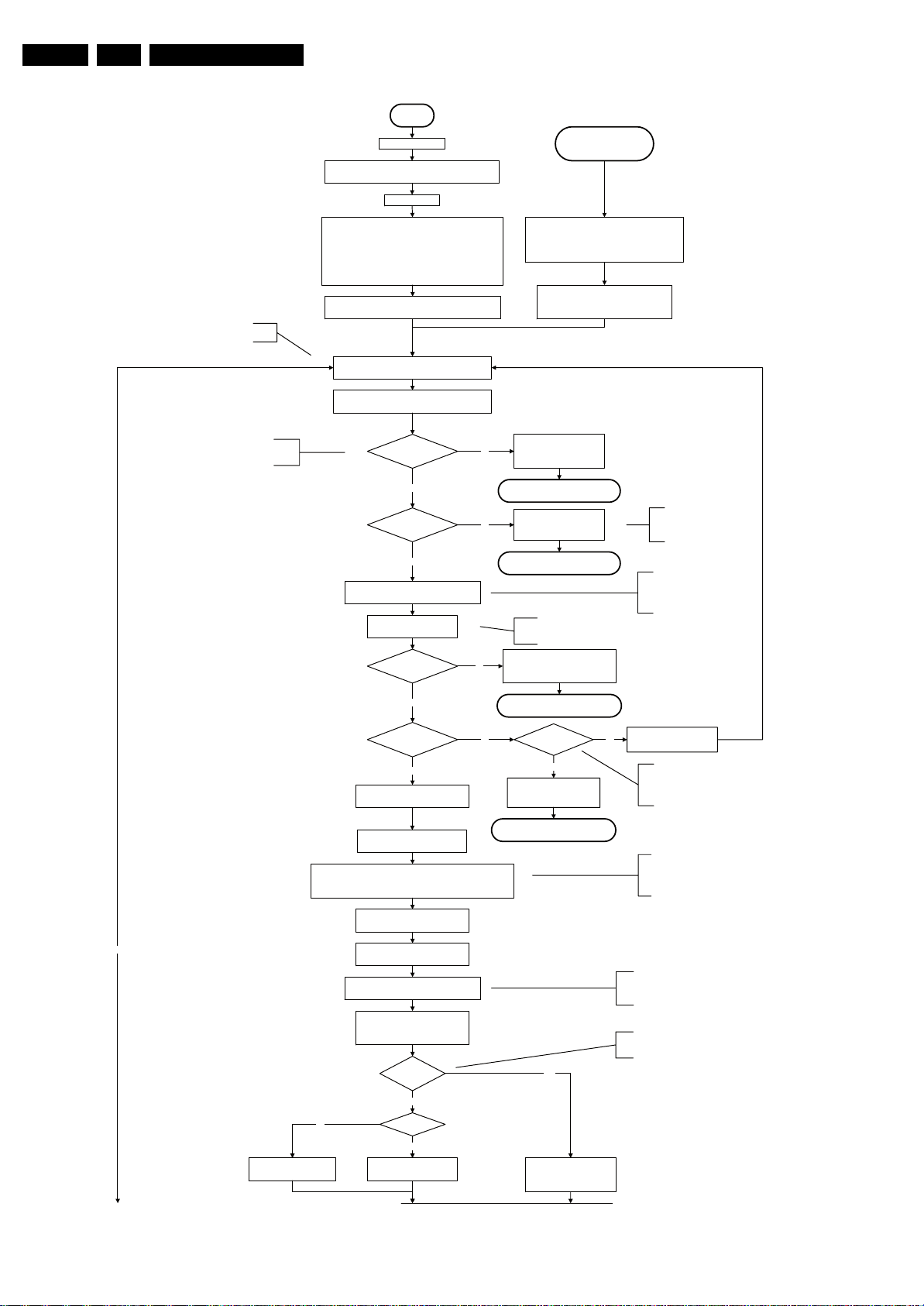
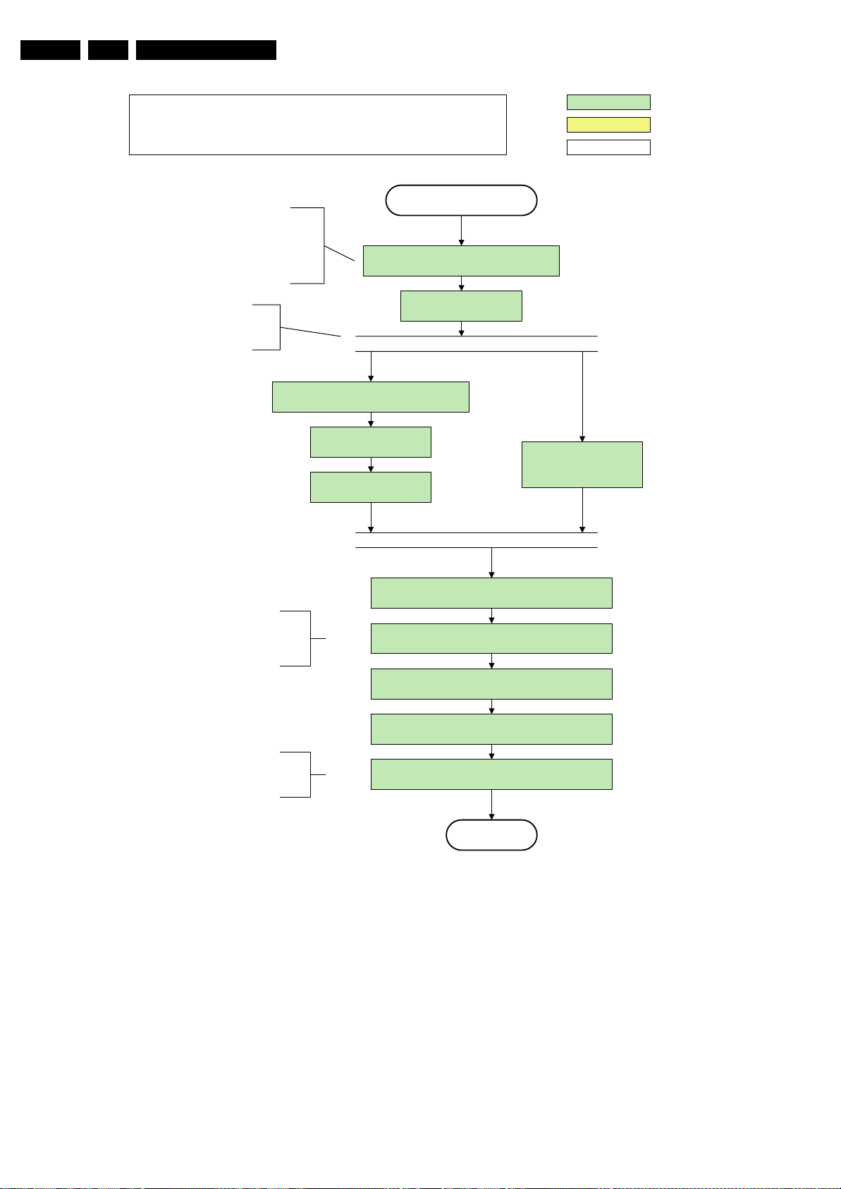
EN 18 Q529.1E LA5.
Important remark; the appearance of the +12V
will start the +1V2 DCDC converter automatically
Service Modes, Error Codes, and Fault Finding
Off
Mains is app lied
Standby Supply star ts running.
All standby supply voltages become available .
st-by µ P resets
Initialise I /O pins of the st -by µP:
- Switch reset-AVCLOW (reset state)
- Switch WP-NandFlash LOW (pr otected)
- Switch reset-system LOW ( reset state)
- Switch reset-5100 LOW (reset state)
- Switch reset-Ethernet LOW (r eset state)
- Switch reset-ST7100 LOW (reset state)
- keep reset-NVM high, Audio-r eset and Audio- Mute- Up HIGH
start keyboard scanning, RC detection. Wake up reasons are
Switch ON Platform and display supply by switching
+12V, +/-12Vs, AL and Bolt- on power
is switched on, followed by the +1V2 DCDC converter
off.
LOW the Standby line .
Stand by or
Protection
If the protection state was left by short circuiting the
SDM pins, detection of a protection condition during
startup will stall the startup . Protection conditions in a
playing set will be ignored . The protection mode will
not be entered.
- Switch Audio -Reset high.
It is low in the standby mode if the standby
mode lasted longer than 10s.
Detect2 should be polled on the standar d 40ms
interval and startup should be continued when
detect2 becomes high.
Switch LOW the RESET- NVM line to allow access to NVM. (Add a
2ms delay before trying to address the NVM to allow corr ect NVM
initialization , this is not issue in this setup , the delay is automatically
No
No
Release AVC system r eset
Feed warm boot script
To I_17660_125b.eps To I_17660_125b.eps
Detect2 high received
within 1 second?
Yes
Supply-fault I/O
High?
Yes
Enable the DCDC converter for +3V3 and
+5V. (EN ABLE-3V3)
Wait 50ms
Supply-fault I/O
High?
yes
Detect-1 I/O line
High?
Yes
Enable the supply fault detection
algorithm
Set I²C slave address
of Standby µP to (A0h)
covered by the architectural setup)
Switch HIGH the WP-NandFlash to
allow access to NAND Flash
Release Reset-PNX5100.
PNX5100 will start b ooting.
Wait 10ms (minimum ) to allow the bootscript
of the PNX5100 to configur e the PCI arbiter
Detect EJTAG debug probe
(pulling pin of the pr obe interface to
ground by inserting EJTAG probe)
EJTAG probe
connected ?
No
Cold boot?
Yes
Relea se AVC system r eset
Feed cold boot script
No
No
No
No
Power-OK er ror:
Layer1: 3
Layer2: 16
Enter protection
1V2 DCDC or class D error:
Layer1: 2
Layer2: 19
Enter protection
Delay of 50ms needed because of the latency of the detect-1 circuit.
This delay is also needed for the PNX5100. The reset of the
PNX5100 should only be r eleased 10ms after pow ering the IC.
3V3 / 5V DCDC or class D er ror:
Layer1: 2
Layer2: 11
Enter protection
Detect -2 I/ O line
High?
Yes
Voltage output error:
Layer1: 2
Layer2: 18
Enter protection
Yes
Release AVC system r eset
Feed initializing boot script
disable alive mechanism
The supply-fault line is a
combination of the DCDC
converters and the audio
protection line.
This enables the +3V3 and
+5V converter. As a result,
also +5V-tuner, +2V5, +1V8PNX8541 and +1V8-PNX5100
become available .
Disable 3V3, swit ch standby
No
line high and wait 4 seconds
Added to make the system mor e robust to
power dips during startup. At this point the
regular supply fault detection algor ithm which
normally detects power dips is not up and
running yet.
This will a llow access to NVM a nd
NAND FLASH and can not be done
earlier because the FLASH needs to
be in Write Protect as long as the
supplies are not available .
Before PNX8541 boots, the PN X5100 should have
set its PCI arbiter (bootscript command). To allow
this, approx. 1ms is needed . This 1ms is extended
to 10ms to also give some relaxation to the supplies.
An EJTAG probe (e.g. WindPower ICE probe) can
be connected for Linux Kernel debugging
purposes.
I_17660_125a.eps
140308
Figure 5-4 “Off” to “Semi Stand-by” flowchart (part 1)
Page 19
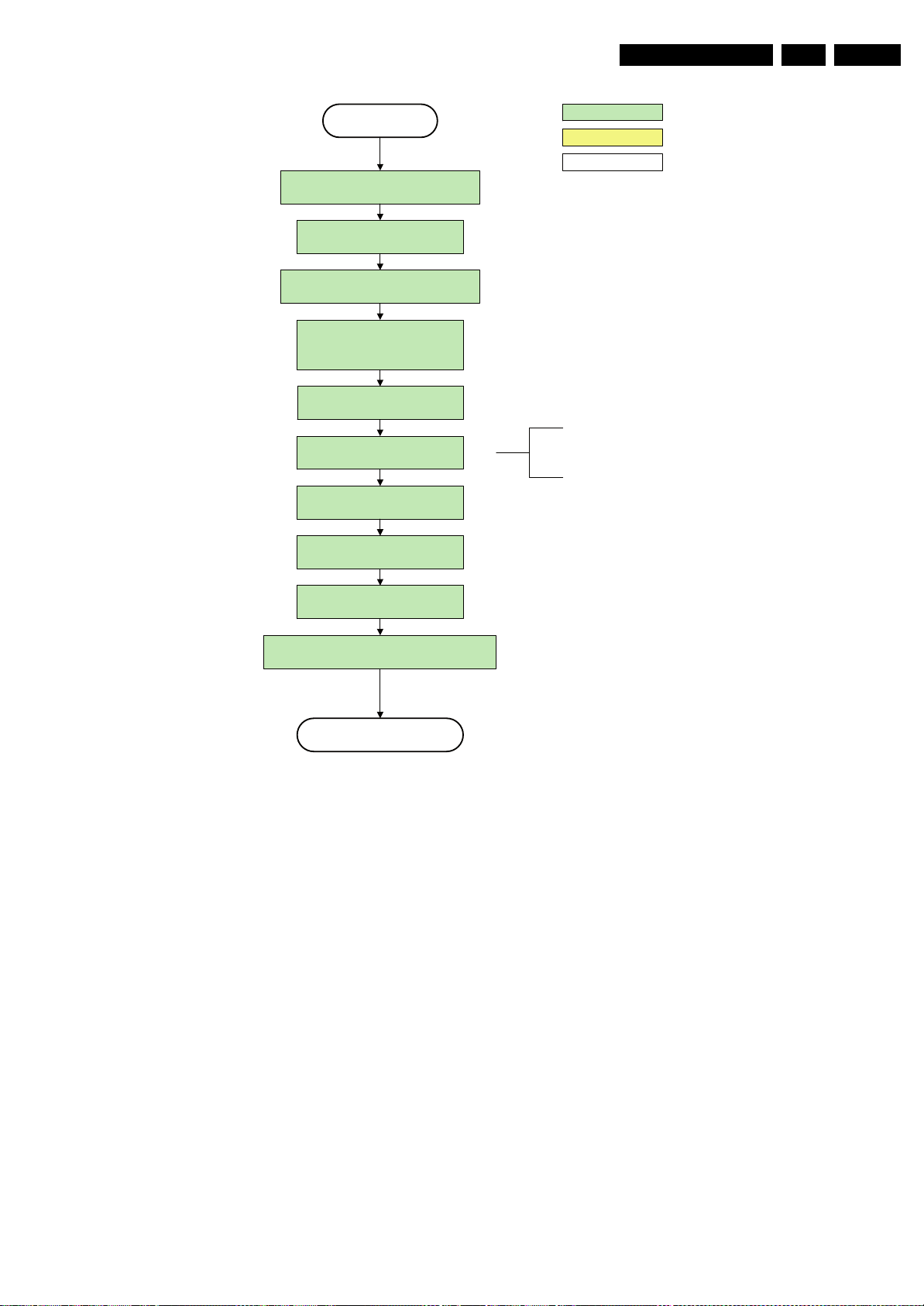
Service Modes, Error Codes, and Fault Finding
From I_17660_125a.eps From I_17660_125a.eps
EN 19Q529.1E LA 5.
No
3-th try?
Yes
Blink Code as
error code
Reset- system is connected to USB
4to1HDMI Mux and channel decoder.
This cannot be done through the bootscript,
the I/O is on the standby µP
Timing need to be updated if
more mature info is available.
Code =
Layer1: 2
Layer2: 15
Switch AVC PNX85 41
in reset (active low )
Wait 10ms
Switch the NVM reset
line HIGH.
Disable all supply related protections and
switch off the +3V3 +5V DC/DC converter.
Wait 5ms
switch off the remaining DC/DC
converters
Switch Standby
I/O line high.
-reset,
No
Code =
Layer1: 2
Layer2: 53
No
Reset-system is switched HIGH by the
AVC at the end of the bootscript
AVC releases Reset-Ethernet when the
end of the AVC boot-script is detected
Reset-Audio and Audio-Mute-Up are
switched by MIPS code later on in the
Set I²C slave address
of Standby µP to (60h)
RPC start (comm. protocol)
No
image transfer succeeded
No
Enable Alive check mechanism
MIPS reads the wake up reason
Switch on the display in case of a LED backlight
display by sending the TurnOnDisplay (1) (I²C)
command to the PNX5100
Download firmware into the channel
startup process
Bootscript ready
in 1250 ms ?
Yes
Flash to Ram
within 30s?
Yes
SW initializatio n
succeeded
within 20s?
Yes
from standby µP.
Initialize audio
decoder
Reset-syst em is switched HIGH by the
AVC at the end of the bootscript
AVC releases Reset-Ethernet when the
end of the AVC boot-script is detected
Reset-Audio and Audio- Mute-Up are
switched by MIPS code later on in the
startup process
Timing needs to
be updated if more
mature info is
available.
Timing needs to be
updated if more
matur e info is
available.
Wait until AVC starts to
communicate
In case of a LED backlight display, a LED DIM panel is
present which is fed by the Vdisplay. To power the LED DIM
Panel, the Vdisplay switch driven by the PNX5100 must be
closed. The display startup sequence is taken care of by the
LED DIM panel.
and generate fast cold reboot
eventually followed by a cold
Alive
polling
NOK
Log SW event
STi7100AliveFailedEr ror
reboot.
Release reset MPEG4 module:
BOLT-ON-IO: High
MPEG4 module will start booting
autonomously.
Wait 3000 ms
POR polling positive ?
yes
Start alive IIC polling
mechanism
No
POR polling positive ?yes
bootSTi7100PorFailure:
and generate cold boot
Log SW event:
STi7100PorFailure
Wait 200 ms
No
Log HW error
Layer1: 2
Layer2: 38
Enter protection
Third try? No
Yes
Log channel decoder error:
Layer1: 2
Layer2: 37
Downloaded
successfully ?
Yes
initialize tuner , Master IF and channel
decoder
Initiali ze source sele ction
Initialize video processing IC 's
initialize AutoTV by triggering CHS AutoTV Init interface
Initialize Ambilight with Lights off.
Semi-Standby
Figure 5-5 “Off” to “Semi Stand-by” flowchart (part 2)
I_17660_125b.eps
140308
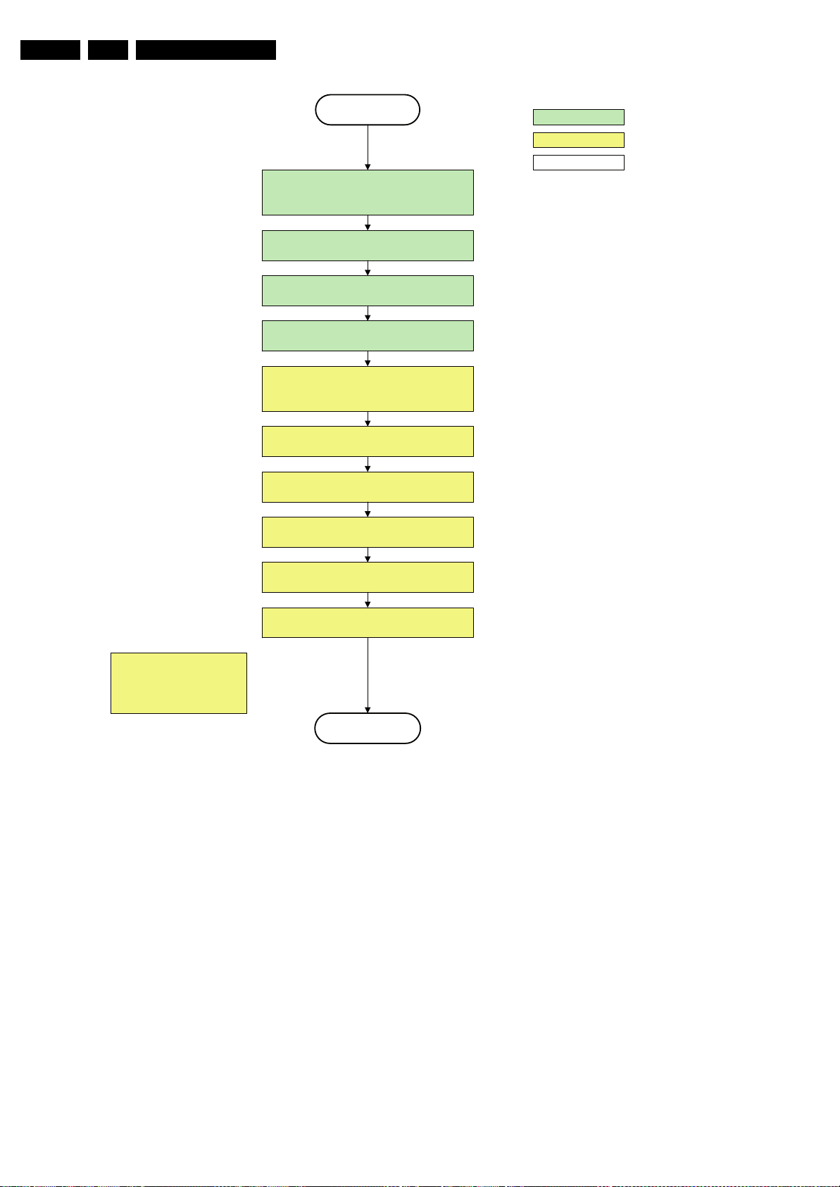
Page 20
EN 20 Q529.1E LA5.
Service Modes, Error Codes, and Fault Finding
Constraints taken into account:
- Display may only be started when valid LVDS output clock can be deliver ed by the AVC .
- Between 5 and 50 ms after power is supplied, display should receive valid lvds clock .
- minimum wait time to switch on the lamp after power up is 200ms.
action holder: AVC
action holder: St-by
autonomous action
The assumption here is that a fast toggle (<2s)
can only happen during ON -> SEMI ->ON. In
these states, the AVC is st ill active and can
provide the 2s delay. If the transition ON-> SEMI-
>STBY -> SEMI ->ON can b e made in less than 2s,
the semi -> stby transition has to be delayed
CPipe already generates a valid output
clock in t he semi -stand by state : display
startup can start immediately when leaving
The timings to be used in
combination with the PanelON
comman d for this specific display
The higher level requirement is that audio and
video should be demuted without transient
effects and that the audio should be demuted
maximum 1s befor e or at the same time as the
until the requirement is met.
the semi-standby state .
TurnOnDisplay(1) (I²C) command to the PNX5100
unblanking of the video .
Semi Standby
Wait until pr evious on -state is left more than 2
seconds ago. (to prevent LCD display pr oblems)
Assert RGB video blanking
Switch on the display by sending the
wait 250ms (min. = 200ms)
Switch on LCD backlight
(Lamp-ON)
Wait until valid and stable audio and video , corresponding to
the requested output is delivered by the AVC.
Switch Audio -R eset low and wait 5ms
Release audio mute and wait 100ms before any other audio
handling is done (e.g. volume change)
and audio mute
Initialize audio and video
processing IC's and functions
according needed use case.
The higher level requirement is that the
ambilight funct ionality may not be switched on
before the backlight is turned on in case the
set contains a CE IPB inverter supply.
Figure 5-6 “Semi Stand-by” to “Active” flowchart
unblank the video.
Switch on the Ambilight functionality according the last status
settings.
Active
I_17660_126.eps
140308
Page 21
Service Modes, Error Codes, and Fault Finding
Constraints taken into account:
- Display may only be started when valid LVDS output clock can be deliver ed by the AVC .
- Between 5 and 50 ms after power is supplied, display should receive valid lvds clock .
- minimum wait time to switch on the lamp after power up is 200ms.
- To have a reliable oper ation of the backlight, the backlight should be driven with a PWM duty cycle of 100%
during the first second. Only after this first one or two seconds, the PWM may be set to the required output level
(Note that the PWM output should be present before the backlight is switched on). To minimize the artefacts, the
picture should only be unblanked after these first seconds .
EN 21Q529.1E LA 5.
action holder: AVC
action holder: St-by
autonomous action
The assumption here is that a fast toggle (<2s)
can only happen during ON->SEMI ->ON. In
these states, the AVC is st ill active and can
provide the 2s delay. If the transition ON -> SEMI-
->ST BY -> SEMI -> ON c an be mad e in less tha n 2s,
the semi -> stby transition has to be delayed
CPipe already generates a valid output
clock in t he semi -standby state: display
startup can start immediately when leaving
until the requirement is met.
the semi-standby state .
Switch on the display by sending the
TurnOnDisplay(1) (I²C) command to the PNX5100
Switch off the dimming backlight feature, set
the BOOST control to nominal and make sur e
Semi Standby
Wait until pr evious on -state is left more than 2
seconds ago. (to prevent LCD display problems)
Assert RGB video blanking
wait 250ms (min. = 200ms)
PWM output is set to 100%
Switch on LC D backlig ht
(Lamp-ON)
and audio mute
Initialize audio and video
processing IC's and functions
according needed use case.
The higher level requirement is that audio and
video should be demuted without transient
effects and that the audio should be demuted
maximum 1s befor e or at the same time as the
unblanking of the video .
The higher level requirement is that the
ambilig ht fun ctionalit y may not be switched on
before the backlight is turned on in case the
set contains a CE IPB inverter supply.
Figure 5-7 “Semi Stand-by” to “Active” flowchart LCD with preheat
Wait until valid and stable audio and video , corresponding to the requested
[the backlight PWM has been on for 1s (internal inverter LPL displays
OR the backlight PWM has been on for 2s (external inver ter LPL displays) ] .
Release audio mute and wait 100ms before any other audio
handling is done (e.g. volume change)
Restore dimming backlight feature, PWM and BOOST output
Switch on the Ambilight functionality according the last status
output is delivered by the AVC
Switch Audio -Reset low and wait 5ms
AND
and unblank the video .
settings.
Active
I_17660_127.eps
140308
Page 22
EN 22 Q529.1E LA5.
Service Modes, Error Codes, and Fault Finding
Constraints taken into account:
- Display may only be started when valid LVDS output clock can be delivered by the AVC .
- Between 5 and 50 ms after power is supplied, display should receive valid lvds clock .
- minimum wait time to switch on the lamp after power up is 200ms.
Semi Standby
The assumption here is that a fast toggle (<2s)
can only happen during ON -> SEMI -> ON. In
these states, the AVC is still act ive and can
provide the 2s delay. If the transition ON -> SEMI-
>STBY->SEMI-> ON can be made in less than 2s,
the semi -> stby transition has to be delayed
CPipe already generates a valid output
clock in t he semi -standby state : d isplay
startup can start immediately when leaving
until the requirement is met.
the semi-standby state .
Switch on the display by sending the OUTPUTENABLE (I²C) command to the LED DIM panel
wait 250ms (min. = 200ms)
Switch on LC D backlig ht
Wait until pr evious on -state is left more than 2
seconds ago. (to prevent LCD display problems)
Assert RGB video blanking
TBC in def. spec
(Lamp-ON)
and audio mute
action holder: AVC
action holder: St-by
autonomous action
Initialize audio and video
processing IC's and functions
according needed use case.
The higher level requirement is that audio and
video should be demuted without transient
effects and that the audio should be demuted
maximum 1s befor e or at the same time as the
unblanking of the video .
The higher level requirement is that the
ambilig ht fun ctionalit y may not be switched on
before the backlight is turned on in case the
set contains a CE IPB inverter supply.
Figure 5-8 “Semi Stand-by” to “Active” flowchart (LED backlight)
Wait until valid and stable audio and video , corresponding to
the requested output is delivered by the AVC.
Switch Audio -R eset low and wait 5ms
Release audio mute and wait 100ms before any other audio
handling is done (e.g. volume change)
unblank the video.
Switch on the Ambilight functionality according the last status
settings.
Active
I_17660_128.eps
140308
Page 23
Service Modes, Error Codes, and Fault Finding
EN 23Q529.1E LA 5.
Active
Mute all sound outputs via softmute
Wait 100ms
Set main amplifier mute (I/O : audio -mute)
Force ext audio outputs to ground
(I/O: audio r eset)
And wait 5ms
switch o ff Ambilig ht
Wait until Ambilight has faded out
(fixed wait time of x s)
switch off LCD backlight
Mute all video outputs
action holder: AVC
action holder: St-by
autonomous action
The higher level requirement is that the
backlight may not be switched off before the
ambilight functionality is tur ned off in case the
set contains a CE IPB inverter supply.
Wait 25 0ms (min . = 200ms)
Switch off the display by sending the
TurnOnDisplay(0) (I²C) command to the PNX5100
Semi Standby
Figure 5-9 “Active” to “Semi Stand-by” flowchart (LCD non DFI)
I_17660_129.eps
140308
Page 24
EN 24 Q529.1E LA5.
Service Modes, Error Codes, and Fault Finding
Semi Stand by
If ambientlight functionality was used in semi -standby
(lampadair e mode), switch off ambient light
Delay transition until ramping down of ambient light is
transfer Wake up reasons to the Stand by µP.
Switch Memories to self-r efresh (this creates a more
stable condition when switching off the power).
Switch AVC syste m in reset sta te
finished. *)
Switch reset-PNX5100 LOW
Switch reset-ST7100 LOW
Switch Reset-Ethernet LOW
Wait 10ms
Switch the NVM reset line HIGH
Switch het WP- Nandflash LOW
action holder: MIPS
action holder: St-by
autonomous action
*) If this is not performed and the set is
switched to standby when the switch off of
the ambilights is still ongoing , the lights will
switch off abruptly when the supply is cut .
Important remark:
release reset audio 10 sec after
entering standb y to save power
Disable all supply related protections and switch off
the DC/DC converters (ENABLE-3V3)
Wait 5ms
Switch OFF all su pplies by swit ching HI GH the
Standby I/O line
Stand by
Figure 5-10 “Semi Stand-by” to “Stand-by” flowchart
I_17660_130.eps
140308
Page 25
Service Modes, Error Codes, and Fault Finding
EN 25Q529.1E LA 5.
action holder: MIPS
action holder: St-by
autonomous action
If needed to speed up this transition,
this block could be omitted. This is
depending on the outcome of the
safety investig ations .
MP
Log the appropriate err or and
set stand-by flag in NVM
Redefine wake up reasons for protection
state and transfer to stand- by µP.
Switch off LCD lamp supply
Wait 250ms (min. = 200ms)
Switch off LVDS signal
Switch off 12V LCD supply within a time frame of
min. 0.5ms to max. 50ms after LVDS switch off.
Ask stand- by µP to enter protection state
Switch AVC in r eset state
SP
Figure 5-11 “To Protection State” flowchart
5.4 Service Tools
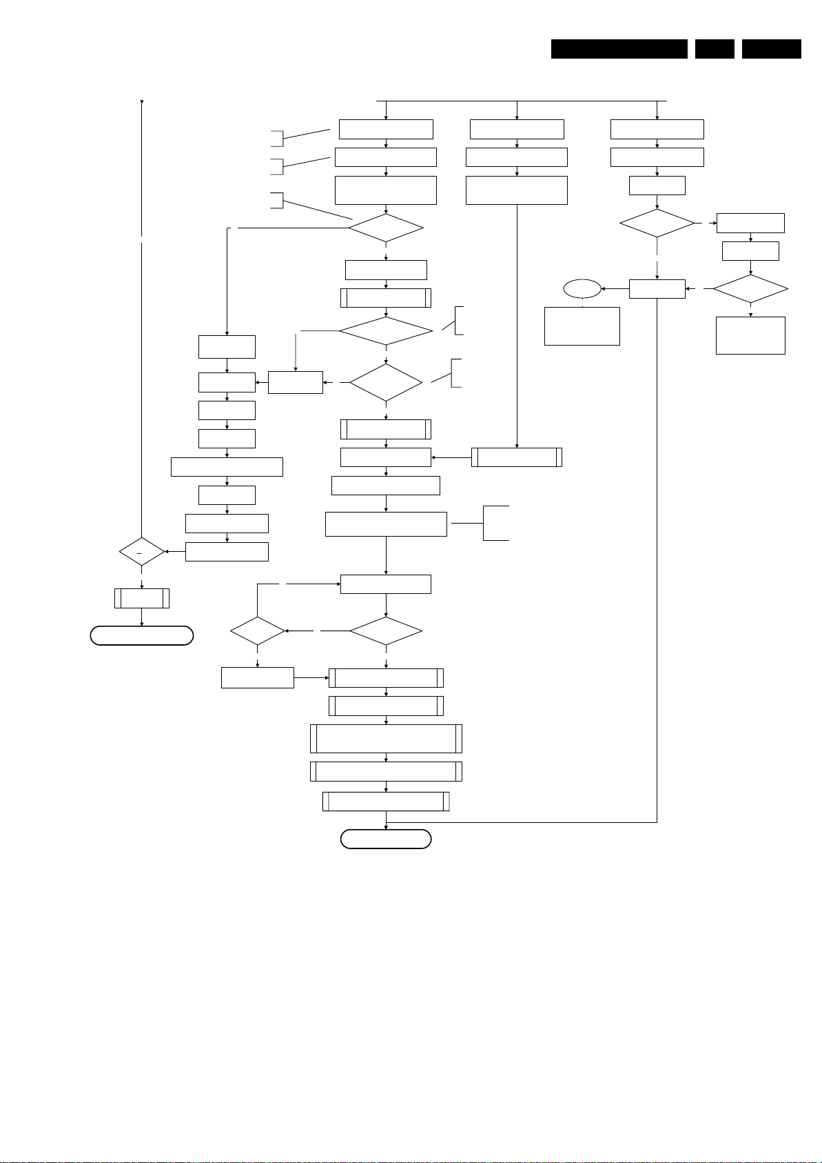
5.4.1 ComPair
Introduction
ComPair (Computer Aided Repair) is a Service tool for Philips
Consumer Electronics products. and offers the following:
1. ComPair helps to quickly get an understanding on how to
repair the chassis in a short and effective way.
2. ComPair allows very detailed diagnostics and is therefore
capable of accurately indicating problem areas. No
knowledge on I
because ComPair takes care of this.
2
C or UART commands is necessary,
Wait 10ms
Switch the NVM reset line HIGH.
Disable all supply related protections and switch off
the +1V8 and the +3V3 DC/DC converter.
Wait 5ms
Switch OF F all supplies by switching HIGH the
Flash the Protection-LED in order to indicate
Standby I/O line .
protection state* (*) : T his can be the standby LED or the ON LED
Protection
3. ComPair speeds up the repair time since it can
automatically communicate with the chassis (when the uP
is working) and all repair information is directly available.
4. ComPair features TV software up possibilities.
Specifications
ComPair consists of a Windows based fault finding program
and an interface box between PC and the (defective) product.
The ComPair II interface box is connected to the PC via an
USB cable. For the TV chassis, the ComPair interface box and
the TV communicate via a bi-directional cable via the service
connector(s).
The ComPair fault finding program is able to determine the
problem of the defective television, by a combination of
automatic diagnostics and an interactive question/answer
procedure.
depending on the availability in the set
I_17660_131.eps
140308
Page 26
EN 26 Q529.1E LA5.
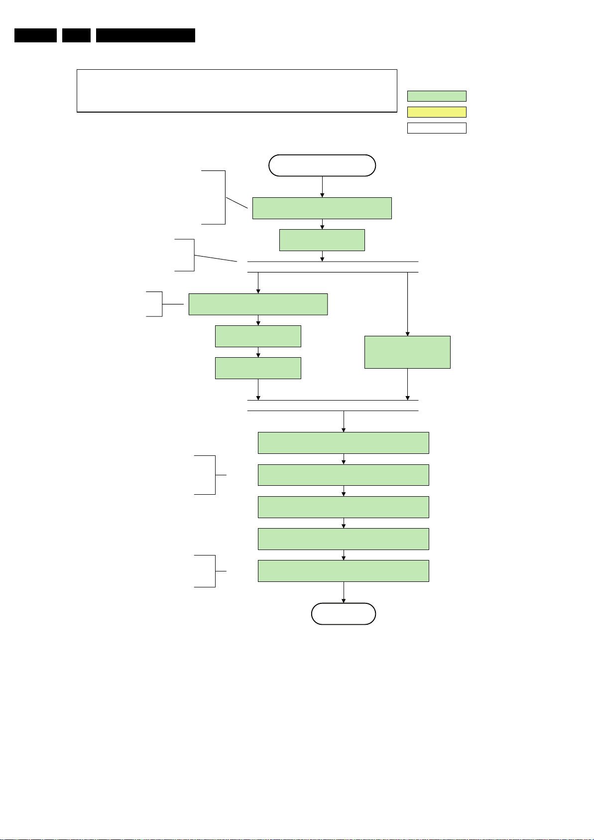
Service Modes, Error Codes, and Fault Finding
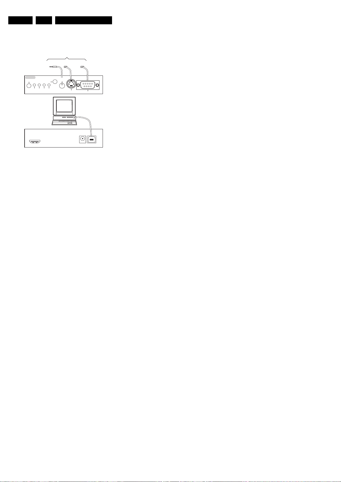
How to Connect
This is described in the chassis fault finding database in
ComPair.
TO TV
TO
UART SERVICE
I2C SERVICE
CONNECTOR
CONNECTOR
2
C
I
PC
ComPair II Developed by Philips Brugge
Optional power
5V DC
TO
RS232 /UART
E_06532_036.eps
150208
ComPair II
RC in
Optional
Switch
Power ModeLink/
Activity
HDMI
2
I
C only
UART SERVICE
RC out
TO
CONNECTOR
Multi
function
Figure 5-12 ComPair II interface connection
Caution: It is compulsory to connect the TV to the PC as
shown in the picture above (with the ComPair interface in
between), as the ComPair interface acts as a level shifter. If
one connects the TV directly to the PC (via UART), ICs will be
blown!
How to Order
ComPair II order codes:
• ComPair II interface: 3122 785 91020.
• Software is available via internet:
http://www.atyourservice.ce.philips.com
• ComPair UART interface cable for Q52x.x.
(using 3.5 mm Mini Jack connector): 3104 311 12742.
Note: While encounting problems, contact the local support
desk.
5.4.2 Memory and Audio Test
With this tool you can test the memory of the PNX8541, as well if the PNX5100 is enabled and audio-testing.
What is needed?
– An USB-stick.
– “TESTSCRIPT Q529” (3104 337 05021). Downloadable
from the Philips Service website from the section “Software
for Service only”.
– A ComPair/service cable (3104 311 12742)
Procedure
Create a directory “JETTFILES” under the root of the USB-stick
– Place “MemoryTestPNX8635.bin” and “autojett.bin”
(available in “TESTSCRIPT Q529”) under the directory
“JETTFILES”
– Install the computer program “BOARDTESTLOGGER”
(available in “TESTSCRIPT Q529”) on the PC
– Connect a “ComPair/service”-cable from the service-
connector in the set to the COM1-port of the PC
– Start-up the program “BOARDTESTLOGGER” and select
“COM1”
– Put the USB stick into the TV and startup the TV while
pressing the “i+”-button on a Philips DVD RC6 remote
control (it’s also possible to use a TV remote in “DVD”mode)
– On the PC the memory test is shown now. This is also
visible on the TV screen.
– In “BOARDTESTLOGGER” an option “Send extra UART
command” can be found where you can select “AUD1”.
This command generates hear test tones of 200, 400,
1000, 2000, 3000, 5000, 8 000 and 12500Hz.
5.4.3 LVDS Tool
Support of this LVDS Tool has been discontinued.
5.5 Error Codes
5.5.1 Introduction
The error code buffer contains all detected errors since the last
time the buffer was erased. The buffer is written from left to
right, new errors are logged at the left side, and all other errors
shift one position to the right.
When an error occurs, it is added to the list of errors, provided
the list is not full. When an error occurs and the error buffer is
full, then the new error is not added, and the error buffer stays
intact (history is maintained).
To prevent that an occasional error stays in the list forever, the
error is removed from the list after more than 50 hrs. of
operation.
When multiple errors occur (errors occurred within a short time
span), there is a high probability that there is some relation
between them.
New in this chassis is the way errors can be displayed:
• There is a simple blinking LED procedure for board level
repair (home repair) so called LAYER 1 errors next to the
existing errors which are LAYER 2 errors.(see table 5-2
error code overview).
– LAYER 1 errors are one digit errors.
– LAYER 2 errors are 2 digit errors.
• In protection mode.
– From consumer mode: LAYER 1.
– From SDM mode: LAYER 2.
• Fatal errors, if I2C bus is blocked and the set reboots,
CSM and SAM are not selectable.
– From consumer mode: LAYER 1.
– From SDM mode: LAYER 2.
Important remark:
For all errors detected by MIPS which are fatal =>
rebooting of the TV set (reboot starts after LAYER error
1 blinking), one should short the solder paths at startup from the power OFF state by mains interruption and
not via the power button to trigger the SDM via the
hardware pins.
• In CSM mode
– When entering CSM: error LAYER 1 will be displayed
by blinking LED. Only the latest error is shown.
• In SDM mode
– When SDM is entered via Remote Control code or the
hardware pins, LAYER 2 is displayed via blinking LED.
• In the ON state
– In “Display error mode”, set with the RC commands
“mute_06250X _OK” LAYER 2 errors are displayed via
blinking LED.
• Error display on screen.
– In CSM no error codes are displayed on screen.
– In SAM the complete error list is shown.
Basically there are three kinds of errors:
• Errors detected by the Stand-by software which lead to
protection. These errors will always lead to protection and
an automatic start of the blinking LED LAYER error 1.
(see section “5.6 The Blinking LED Procedure”).
• Errors detected by the Stand-by software which not
lead to protection. In this case the front LED should blink
the involved error. See also section “5.5 Error Codes, 5.5.4
Error Buffer, Extra Info”. Note that it can take up several
minutes before the TV starts blinking the error (e.g. LAYER
error 1 = 2, LAYER error 2 = 15 or 53).
Page 27

Service Modes, Error Codes, and Fault Finding
• Errors detected by main software (MIPS). In this case
the error will be logged into the error buffer and can be read
out via ComPair, via blinking LED method LAYER error 12, or in case picture is visible, via SAM.
5.5.2 How to Read the Error Buffer
Use one of the following methods:
• On screen via the SAM (only when a picture is visible).
E.g.:
– 00 00 00 00 00: No errors detected
– 23 00 00 00 00: Error code 23 is the last and only
detected error.
– 37 23 00 00 00: Error code 23 was first detected and
error code 37 is the last detected error.
– Note that no protection errors can be logged in the
error buffer.
• Via the blinking LED procedure. See section 5.5.3 How to
Clear the Error Buffer.
•Via ComPair.
5.5.3 How to Clear the Error Buffer
Use one of the following methods:
• By activation of the “RESET ERROR BUFFER” command
in the SAM menu.
• With a normal RC, key in sequence “MUTE” followed by
“062599” and “OK”.
• If the content of the error buffer has not changed for 50+
hours, it resets automatically.
EN 27Q529.1E LA 5.
5.5.4 Error Buffer
In case of non-intermittent faults, clear the error buffer before
starting to repair (before clearing the buffer, write down the
content, as this history can give significant information). This to
ensure that old error codes are no longer present.
If possible, check the entire contents of the error buffer. In
some situations, an error code is only the result of another error
code and not the actual cause (e.g. a fault in the protection
detection circuitry can also lead to a protection).
There are several mechanisms of error detection:
• Via error bits in the status registers of ICs.
• Via polling on I/O pins going to the stand-by processor.
• Via sensing of analog values on the stand-by processor or
the PNX8541.
• Via a “not acknowledge” of an I
Take notice that some errors need several minutes before they
start blinking or before they will be logged. So in case of
problems wait 2 minutes from start-up onwards, and then
check if the front LED is blinking or if an error is logged.
2
C communication.
Page 28
EN 28 Q529.1E LA5.
Table 5-2 Error code overview
Service Modes, Error Codes, and Fault Finding
Description Layer 1 Layer 2
2
C3 2 13 MIPS E BL / EB SCL/D-SSB SSB
I
2
C4 5 14 MIPS E BL / EB SCL/D-DISP Display (LED back light only)
I
by
PNX doesn’t boot (HW cause) 2 15 Stby µP E BL PNX8541 I
Monitored
Error/
Error Buffer/
Prot
Blinking LED Device Defective Board
2
C blocked SSB
12V 3 16 Stby µP P BL / Supply
1V2, 3V3, 5V to low 2 18 Stby µP P BL / SSB
1V2 or Class D 2 19 Stby µP P BL / SSB
3V3/5V DCDC to high 2 11 Stby µP P BL / SSB
PNX 5100 2 21 MIPS E EB PNX5100 SSB
HDMI mux 2 23 MIPS E EB AD8197A SSB
2
C switch 2 24 MIPS E EB PCA9540 SSB
I
Master IF 2 26 MIPS E EB TDA9898 SSB
FPGA Ambilight 2 28 MIPS E EB / SSB
Tuner 2 34 MIPS E EB UV1783S/TD1716 SSB
Channel Decoder DVB-T 2 37 MIPS E EB TDA10048 SSB
ST7100 2 38 MIPS E EB ST7100 SSB
MHP 6 39 MIPS E EB / MHP module
Fan I2C expander 7 41 MIPS E EB PCA9533 FAN module
T° sensor 7 42 MIPS E EB LM 75 T° sensor
FAN 1 7 43 MIPS E EB FAN
FAN 2 7 44 MIPS E EB FAN
main NVM 2 / MIPS E X STM24C128 SSB
Channel decoder DVB-C 2 48 MIPS E EB TDA 10023 SSB
PNX doesn’t boot (SW cause) 2 53 Stby µP E BL PNX8541 SSB
Display (only LED back light) 5 64 MIPS E BL / EB Display
Extra Info
• Rebooting. When a TV is constantly rebooting due to
internal problems, most of the time no errors will be logged
or blinked. This rebooting can be recognized via a ComPair
interface and Hyperterminal (for Hyperterminal settings,
see section “5.8 Fault Finding and Repair Tips, 5.8.6
Logging). It’s shown that the loggings which are generated
by the main software keep continuing. In this case
diagnose has to be done via ComPair.
• Error 11 (3V3/5V too high). This protection can occur
during start up (LAYER error 1 = 2). Be careful to overrule
this protection via SDM for the reason supply related
devices can be possibly destroyed here.
• Error 13 (I
2
C bus 3 blocked). At the time of release of this
manual, this error was not working as expected. Current
situation: when this error occurs, the TV will constantly
reboot due to the blocked bus. The best way for further
diagnosis here, is to use ComPair.
• Error 15 (PNX8541 doesn’t boot). Indicates that the main
processor was not able to read his bootscript. This error will
point to a hardware problem around the PNX8541
(supplies not OK, PNX 8541 completely dead, I
between PNX and Stand-by Processor broken, etc...).
When error 15 occurs it is also possible that I
blocked (NVM). I
2
C2 can be indicated in the schematics as
2
C link
2
C2 bus is
follows: SCL-UP-MIPS, SDA-UP-MIPS, SCL-2 or SDA-2.
Other root causes for this error can be due to hardware
problems with : NVM PNX5100, PNX5100 itself, DDR’s.
• Error 16 (12V). This voltage is made in the power supply
and results in protection (LAYER error 1 = 3) in case of
absence. When SDM is activated we see blinking LED
LAYER error 2 = 16.
• Error 18 (1V2-3V3-5V too low). All these supplies are
generated by the DC/DC supply on the SSB. If one of these
supplies is too low, protection occurs and blinking LED
LAYER error 1 = 2 will be displayed automatically. In SDM
this gives LAYER error 2 = 18.
• Error 19 (1V2 or class D). This is an combination of two
detections:
– If one of the 1V2 supplies is too high or too low in the
start up procedure the supply fault becomes low.
– If a DC voltage occurs on the output of the Class D
amplifier the supply fault becomes low. Be careful to
overrule this protection via SDM, check audio part first
before apply. In case one of the speakers is not
connected, the protection can also be triggered.
• Error 21 (PNX 5100). At the time of release of this manual,
this error was not working as expected. Current situation:
when this error occurs, the TV will constantly reboot. This
rebooting can be recognized via a ComPair interface and
Hyperterminal (for Hyperterminal settings, see section “5.8
Fault Finding and Repair Tips, 5.8.6 Logging”). It is shown
that the loggings which are generated by the main software
keep continuing. The best way for further diagnosis here, is
to use ComPair.
• Error 21 (PNX 5100). At the time of release of this manual,
this error was not working as expected. Current situation:
when there is no I
2
C communication towards the PNX5100
after startup (power off by disconnection of the mains
cord), LAYER error 2 will blink continuously via the blinking
LED procedure in SDM. (startup the TV with the solder
paths short to activate SDM).
• Error 23 (HDMI). When there is no I
2
C communication
towards the HDMI mux after start up, LAYER error 2 = 23
will be logged and displayed via the blinking LED
procedure if SDM is switched on.
• Error 26 (Master IF). When there is no I
2
C communication
towards the Master IF after start up, LAYER error 2 = 26
will be logged and displayed via the blinking LED
procedure when SDM is switched on.
• Error 28 (FPGA ambilight). When there is no I
2
C
communication towards the FPGA ambilight after start up,
LAYER error 2 = 28 will be logged and displayed via the
blinking LED procedure if SDM is switched on. Note that it
can take up several minutes before the TV starts blinking
LAYER error 1 = 2 in CSM or in SDM, LAYER error 2 = 28.
• Error 34 (Tuner). When there is no I
2
C communication
towards the tuner after start up, LAYER error 2 = 34 will be
Page 29

Service Modes, Error Codes, and Fault Finding
EN 29Q529.1E LA 5.
logged and displayed via the blinking LED procedure when
SDM is switched on.
• Error 37 (Channel decoder DVBT). When there is no I
communication towards the DVBT channel decoder after
start up, LAYER error 2 = 37 will be logged and displayed
via the blinking LED procedure if SDM is switched on.
• Error 38 (STI7100). When there is no I
2
C communication
towards the STI7100 after startup (power off by
disconnection of the mains cord), LAYER error 2 = 38 will
be logged and displayed via the blinking LED procedure in
SDM (startup the TV with the solder paths short to activate
SDM). Remark : if the error occurs during the ON state, the
TV will constantly reboot and no LED blinking will be
displayed. This rebooting can be recognized via a ComPair
interface and Hyperterminal (for Hyperterminal settings,
see section “5.8 Fault Finding and Repair Tips, 5.8.6
Logging”). It is shown that the loggings which are
generated by the main software keep continuing. Check in
the logging for keywords like e.g. “Device error 38”.
• Main NVM. When there is no I
2
C communication towards
the main NVM, LAYER error 1 = 2 will be displayed via the
blinking LED procedure. In SDM, LAYER error 2 can be 19.
Check the logging for keywords like “I
2
C bus blocked”.
• Error 48 (Channel decoder DVBC). When there is no I
communication towards the DVBC channel decoder after
start up, LAYER error 2 = 48 will be logged and displayed
via the blinking LED procedure while SDM is active.
• Error 53. This error will indicate that the PNX8541 has
read his bootscript (when this would have failed, error 15
would blink) but initialization was never completed because
of hardware problems (NAND flash, ...) or software
initialization problems. Possible cause could be that there
is no valid software loaded (try to upgrade to the latest main
software version). Note that it can take up to 2 minutes
before the TV starts blinking LAYER error 1 = 2 or in SDM,
LAYER error 2 = 53.
5.6 The Blinking LED Procedure
5.6.1 Introduction
The blinking LED procedure can be split up into two situations:
• Blinking LED procedure LAYER error 1. In this case the
error is automatically blinked when the TV is put in CSM.
This will be only one digit error, namely the one that is
referring to the defective board (see table “Table 5-2 Error
code overview”) which causes the failure of the TV. This
approach will especially be used for home repair and call
centres. The aim here is to have service diagnosis from a
distance.
• Blinking LED procedure LAYER error 2. Via this procedure,
the contents of the error buffer can be made visible via the
front LED. In this case the error contains 2 digits (see table
“Table 5-2 Error code overview”) and will be displayed
when SDM (hardware pins) is activated. This is especially
useful for fault finding and gives more details regarding the
failure of the defective board.
Important remark:
For all errors detected by MIPS which are fatal =>
rebooting of the TV set (reboot starts after LAYER error 1
blinking), one should short the solder paths at start-up from
the power OFF state by mains interruption and not via the
power button to trigger the SDM via the hardware pins.
When one of the blinking LED procedures is activated, the front
LED will show (blink) the contents of the error-buffer. Error
codes greater then 10 are shown as follows:
1. “n” long blinks (where “n” = 1 to 9) indicating decimal digit
2. A pause of 1.5 s
3. “n” short blinks (where “n”= 1 to 9)
4. A pause of approximately 3 s,
5. When all the error codes are displayed, the sequence
2
C
finishes with a LED blink of 3 s
6. The sequence starts again.
Example: Error 12 8 6 0 0.
After activation of the SDM, the front LED will show:
1. One long blink of 750 ms (which is an indication of the
decimal digit) followed by a pause of 1.5 s
2. Two short blinks of 250 ms followed by a pause of 3 s
3. Eight short blinks followed by a pause of 3 s
4. Six short blinks followed by a pause of 3 s
5. One long blink of 3 s to finish the sequence
6. The sequence starts again.
5.6.2 How to Activate
Use one of the following methods:
• Activate the CSM. The blinking front LED will show only
the latest layer error 1, this works in “normal operation”
mode or automatically when the error/protection is
monitored by the standby processor. At the time of this
release, this layer error 1 blinking was not working as
2
C
expected.
In case no picture is shown and there is no LED blinking, n
read the logging to detect whether “error devices” are
mentioned. (see section “5.8 Fault Finding and Repair
Tips, 5.8.6 Logging”).
• Activate the SDM. The blinking front LED will show the
entire contents of the layer error 2 buffer, this works in
“normal operation” mode or when SDM (via hardware pins)
is activated when the tv set is in protection.
Important remark:
For all errors detected by MIPS which are fatal =>
rebooting of the TV set (reboot starts after LAYER error 1
blinking), one should short the solder paths at start-up from
the power OFF state by mains interruption and not via the
power button to trigger the SDM via the hardware pins.
• Transmit the commands “MUTE” - “062500” - “OK”
with a normal RC. The complete error buffer is shown.
Take notice that it takes some seconds before the blinking
LED starts.
• Transmit the commands “MUTE” - “06250x” - “OK”
with a normal RC (where “x” is a number between 1
and 5). When x = 1 the last detected error is shown, x = 2
the second last error, etc.... Take notice that it takes some
seconds before the blinking LED starts.
5.7 Protections
5.7.1 Software Protections
Most of the protections and errors use either the stand-by
microprocessor or the MIPS controller as detection device.
Since in these cases, checking of observers, polling of ADCs,
and filtering of input values are all heavily software based,
these protections are referred to as software protections.
There are several types of software related protections, solving
a variety of fault conditions:
• Protections related to supplies: check of the 12V, +5V,
+3V3 and 1V2.
• Protections related to breakdown of the safety check
mechanism. E.g. since the protection detections are done
by means of software, failing of the software will have to
initiate a protection mode since safety cannot be
guaranteed any more.
Remark on the Supply Errors
The detection of a supply dip or supply loss during the normal
playing of the set does not lead to a protection, but to a cold
reboot of the set. If the supply is still missing after the reboot,
the TV will go to protection.
Page 30

EN 30 Q529.1E LA5.
Service Modes, Error Codes, and Fault Finding
Protections during Start-up
During TV start-up, some voltages and IC observers are
actively monitored to be able to optimise the start-up speed,
and to assure good operation of all components. If these
monitors do not respond in a defined way, this indicates a
malfunction of the system and leads to a protection. As the
observers are only used during start-up, they are described in
the start-up flow in detail (see section “5.3 Stepwise Start-up”).
5.7.2 Hardware Protections
The only real hardware protection in this chassis appears in
case of an audio problem e.g. DC voltage on the speakers. The
audio protection circuit pulls the “supply-fault” low and the tv set
will blink LAYER error 1 = 2 or in SDM, LAYER error 2 = 19. Be
very careful to overrule this protection via SDM (not to cause
damage to the Class D audio amplifier). Check audio part first
before activating via SDM. In case one of the speakers is not
connected, the protection can also be triggered.
Repair Tips
• It is also possible that the set has an audio DC protection
because of an interruption in one or both speakers (the DC
voltage that is still on the circuit cannot disappear through
the speakers). Caution: (Dis)connecting the speakers
during the ON state of the TV can damage the audio
amplifier.
5.7.3 Important remark regarding the blinking LED indication
As for the blinking LED indication, the blinking led of error
layer 1 displaying can be switched off by pushing the power
button on the keyboard.
This condition is not valid after the set was unpowered (via
mains interruption). The blinking LED starts again and can only
be switched off by unplugging the mains connection.
This can be explained by the fact that the MIPS can not load
the keyboard functionality from software during the start-up and
doesn’t recognizes the keyboard commands at this time.
5.8 Fault Finding and Repair Tips
Read also section “5.5 Error Codes, 5.5.4 Error Buffer, Extra
Info”.
Caution: For the whole platform the speaker connections are
grounded on -12 V level. During service measurements with
earth grounded equipment like e.g. scope, great risk of using
the speaker terminal connections for earth ground is currently
present. One will short circuit the -12 V to earth ground in that
way and will causes damage of the supply/audio part!
5.8.1 Ambilight
Due to degeneration process of the AmbiLights, there can be a
difference in the colour and/or light output of the spare
ambilight module in comparison with the originals ones
contained in the TV set. Via ComPair the light output can be
adjusted.
5.8.2 Audio Amplifier
The Class D-IC 7D10 has a powerpad for cooling. When the IC
is replaced it must be ensured that the powerpad is very well
pushed to the PCB while the solder is still liquid. This is needed
to insure that the cooling is guaranteed, otherwise the Class DIC could break down in short time.
5.8.3 CSM
When CSM is activated and there is a USB stick connected to
the TV, the software will dump the complete CSM content to the
USB stick. The file (Csm.txt) will be saved in the root of the USB
stick. If this mechanism works it can be concluded that a large
part of the operating system is already working (MIPS, USB...)
5.8.4 DC/DC Converter
Introduction
The onboard supply consists of 5 DC/DC converters and 7
linear stabilizers. The DC/DC converters have all +12V input
voltage and deliver:
1. +1V2-PNX8541 supply voltage, stabilized close to
PNX8541 chip.
2. +1V2-PNX5100 supply voltage, stabilized close to
PNX5100 chip.
3. +3V3 (overall 3.3 V for onboard IC’s).
4. +5V for USB and Conditional Access Interface and +5V5TUN tuner stabilizer.
5. +33VTUN for analog only tuners (AP diversity).
The linear stabilizers are providing:
1. +1V supply voltage (out of +1V2-PNX8541), stabilized
close to ST7101 chip (MPEG4 diversity).
2. +1V8-PNX5100.
3. +1V8-PNX8541 (reserved because +1V8-PNX5100 used
also for DDR2 interface of PNX8541 via 5FB0).
4. +2V5 (MPEG4 diversity).
5. +1V2-STANDBY (out of +3V3-STANDBY).
6. +5V-TUN (out of +5V5-TUN).
7. +3V3-STANDBY (out of +12V, reserved).
+3V3-STANDY and +1V2-STANDBY are permanent voltages.
Supply voltages +1V2-PNX8541, +1V2-PNX5100 and +1V are
started immediately when +12V incoming voltage is available
(+12V is enabled by STANDBY signal, active low). Supply
voltages +3V3, 2V5, +1V8-PNX5100, +1V8-PNX8541, +5V
and +5V-TUN are switched-on directly by signal ENABLE-3V3
(active low) when +12V and previous mentioned voltages are
all available.
Debugging
The best way to find a failure in the DC/DC converters is to
check their starting-up sequence at power-on via the mains
cord, presuming that the standby microprocessor and the
external supply are operational. Take STANDBY signal highto-low transition as reference.
When +12V rises above 10V then +1V2-PNX8541, +1V2PNX5100 and +1V are started immediately. Then, after
ENABLE-3V3 goes low, all the other supply voltages should
rise within 10 ms. Boost voltages should be OK when +1V2PNX8541, +1V2-PNX5100 are available (FU07 and FU8A,
around 19V).
SUPPLY-FAULT signal should be high when all supply
voltages are started-up.
Tips
• Usually, when supply voltage is short-circuited to GND, the
corresponding DC/DC converter is making audible noise.
• The drop voltage across resistors 3U70 and 3U3T is
100 mV to 2000 mV.
• Defective (in short-circuit) power MOS-FET’s lead usually
to their controller IC broken; if one or more high-side MOSFET’s (7U05, 7U08, 7U0D-1 or 7U0H-1) is broken then the
platform can be heavily damaged if started in SDM-mode
(SUPPLY-FAULT signal is then ignored, while higher than
normal supplies will be generated).
• The +33VTUN generator circuit (7U0P + 7U0Q +
surrounding components) has low output current
capability. In case of too low or no output voltage check
transistor 7U0P (gate voltage pulses of about 10 V
amplitude and drain voltage pulses of about 35 V
amplitude) and the load (not more than 4.5 mA).
Page 31

Service Modes, Error Codes, and Fault Finding
EN 31Q529.1E LA 5.
• High output ripple voltage of DC/DC converters can be
caused by defective (cracked or bad soldered) ceramic
capacitors in the feedback (DC or AC) input or output
filtering.
5.8.5 Exit “Factory Mode”
When an “F” is displayed in the screen's right corner, this
means that the set is in “Factory” mode, and it normally
happens after a new SSB has been mounted.
To exit this mode, push the “VOLUME minus” button on the
TV's keyboard control for 5 seconds and restart the set.
5.8.6 Logging
When something is wrong with the TV set (f.i.the set is
rebooting) you can check for more information via the logging
in Hyperterminal. The Hyperterminal is available in every
Windows application via Programs, Accessories,
Communications, Hyperterminal. Connect a “ComPair UART”cable (3104 311 12742) from the service connector in the TV
set to the “COM1”-port of the PC. After start-up of the
Hyperterminal, fill in a name (f.i. “logging”) in the “Connection
Description” box, then apply the following settings:
1. COM1
2. Bits per second = 38400
3. Data bits = 8
4. Parity = none
5. Stop bits = 1
6. Flow control = none
During the start-up of the TV set, the logging will be displayed.
This is also the case during rebooting of the TV set (the same
logging appears time after time). Also available in the logging
is the “Display Option Code” (useful when there is no picture),
look for item “DisplayRawNumber” in the beginning of the
logging. Tip: when there is no picture available during rebooting
you are able to check for “error devices” in the logging (LAYER
2 error) which can be very helpful to determine the failure cause
of the reboot. For protection state, there is no logging.
5.8.11 UI over PCI bus
The UI is not integrated in the RGB signal but is send from
PNX8541 to PNX5100 via the PCI bus. TXT and MHEG are
integrated in the RGB signal. So when TXT signal is available
but no UI, check the PCI bus.
5.8.12 Display option code
Attention: In case the SSB is replaced, always check the
display option code in SAM, even when picture is available.
Performance with the incorrect display option code can lead to
unwanted side-effects for certain conditions.
5.8.13 Upgrade EDID NVM
To upgrade the EDID NVM pin 7 of the EDID NVM has to be
short circuited to ground. Therefore some test points are
foreseen (figure “EDID-NVM pins”). See ComPair for further
instructions.
X530EDID2
X530EDID1
X530EDID3
X530EDID4
I_17660_119.eps
140308
5.8.7 Loudspeakers
Make sure that the volume is set to minimum during
disconnecting the speakers in the ON-state of the TV. The
audio amplifier can be damaged by disconnecting the speakers
during ON-state of the set! Sometimes the set can go into
protection, but that is not always the case. Caution: On a ME8styling set (74xx or 76xx-range) with removed back cover the
loudspeakers are automatically disconnected!
5.8.8 IPB
In case of no picture when CSM-test pattern from PNX5100 is
displayed and backlight doesn’t light up, It’s recommended first
to check the inverter on the IPB + wiring before replacing the
hole display!
5.8.9 Sanken display supply
The 52” sets in this chassis come with a Sanken buy-in supply.
When the primary circuit of the platform supply fails, there is a
high possibility that the main fuse of the Sanken display supply
will break. In this case the Sanken supply must not be replaced
completely, just replace the Sanken main value fuse and repair
the platform supply. For safety reasons, make sure to use the
correct fuse type.
5.8.10 Tuner
Figure 5-13 EDID-NVM pins
Attention: In case the tuner is replaced, always check the tuner
options!
Page 32

EN 32 Q529.1E LA5.
5.8.14 SSB Replacement
Follow the instructions in the flowchart in case you have to
exchange the SSB. See figure “SSB replacement flowchart”.
Service Modes, Error Codes, and Fault Finding
START
Set is still
operating?
Set is starting up but no display
Upgrade main TV SW to the latest version via
USB stick (#)
Program “Display Option” code via 062598
MENU, followed by 3 digits code (this code
can be found on a sticker inside the set or in
the Service Manual)
After entering “Display Option” code, set is
going to Standby (= validation of code)
Restart the set
Yes
No
Activate SAM and save the TV settings
via “Upload to USB”
- Replace SSB board by a Service SSB.
- Make the SSB fit mechanically to the set.
Start-up set
If necessary, adapt the connector plate and/or
the shielding to make the assy fit
mechanically.
Set behaviour?
Set is starting up & display is OK
Set goes into protection
Activate SDM via shorting the Service pins on
the SSB
- Program Display Option code via 062598 MENU followed by the 3 digit code
(see sticker inside set or in the Service Manual)
- Or program “Display Option” code in SAM via “062596 i+”, Options, Display, Screen
Method 1; In some sets it is possible to
program “Display Option” code before set is
going into protection.
If set is starting-up in Factory mode “F”, push
the “Volume minus” button on the local
keyboard for 5 seconds and restart the set
Method 2; First bring set in SDM and
program “Display Option” code.
Method 3; Bring the PDP power supply in
stand-alone mode and program the “Display
Option” code.
No
Connect ComPair, load JETT software and
program set type- and serial number
Update main and Standby software via USB
(#) Some new “Display Option” codes are not recognised
by SSB’s with old(er) SW, resulting in “no display”.
Therefore it is advised to ALWAYS update the main TV
SW (autorun.upg) via a USB stick to the latest version,
before setting the “Display Option” code
.
Figure 5-14 SSB replacement flowchart
Saved settings
on USB stick?
Yes
Activate SAM and reload settings
via “Download from USB”
Check latest software on Service website.
Check and perform alignments in SAM
according to the Service Manual
Check changes in CSM
END
In case of settings reloaded from USB, the set type- and
set serial number are automatically stored when entering
display options.
- Check if correct “Display Option” code is programmed.
- Verify “Option Codes” according sticker inside the set.
- Default settings for White drive ...see Service Manual
Instruction note SSB replacement
3122 785 00982
05-FEB-2007
H_16771_007.eps
130707
Page 33

Service Modes, Error Codes, and Fault Finding
EN 33Q529.1E LA 5.
5.9 Software Upgrading
5.9.1 Introduction
The set software and security keys are stored in a NANDFlash, which is connected to the PNX8541 via the PCI bus.
It is possible for the user to upgrade the main software via the
USB port. This allows replacement of a software image in a
stand alone set, without the need of an E-JTAG debugger. A
description on how to upgrade the main software can be found
in the DFU.
Important: When the NAND-Flash must be replaced, a new
SSB must be ordered, due to the presence of the security keys!
(copy protection keys, MAC address, ...). It is however also
possible to replace the NAND-Flash with a good one from a
scrap-board.
Perform the following actions after SSB replacement:
1. Set the correct option codes (see sticker inside the TV).
2. Update the TV software (see the DFU for instructions).
3. Perform the alignments as described in chapter 8 (section
“Reset of Repaired SSB”).
4. Check in CSM if the HDMI keys are valid.
For the correct order number of a new SSB, always refer to the
Spare Parts list!
5.9.2 Main Software Upgrade
• The “UpgradeAll.upg” file is only used in the factory.
• The “FlashUtils.upg” file is only used by service centra
which are allowed to do component level repair on the
SSB.
Automatic Software Upgrade
In “normal” conditions, so when there is no major problem with
the TV, the main software and the default software upgrade
application can be upgraded with the “AUTORUN.UPG”
(FUS part of the one-zip file: e.g. 3104 337 04731 _FUS
_Q591E_ 1.25.5.0_commercial.zip). This can also be done by
the consumers themselves, but they will have to get their
software from the commercial Philips website or via the
Software Update Assistant in the user menu (see DFU). The
“autorun.upg” file must be placed in the root of the USB stick.
How to upgrade:
1. Copy “AUTORUN.UPG” to the root of the USB stick.
2. Insert USB stick in the set while the set is in ON MODE.
The set will restart and the upgrading will start
automatically. As soon as the programming is finished, a
message is shown to remove the USB stick and restart the
set.
Manual Software Upgrade
In case that the software upgrade application does not start
automatically, it can also be started manually.
How to start the software upgrade application manually:
1. Disconnect the TV from the Mains/AC Power.
2. Press the “OK” button on a Philips TV remote control or a
Philips DVD RC-6 remote control (it is also possible to use
a TV remote in “DVD” mode). Keep the “OK” button
pressed while reconnecting the TV to the Mains/AC Power.
3. The software upgrade application will start.
Attention!
In case the download application has been started manually,
the “autorun.upg” will maybe not be recognized.
What to do in this case:
1. Create a directory “UPGRADES” on the USB stick.
2. Rename the “autorun.upg” to something else, e.g. to
“software.upg”. Do not use long or complicated names,
keep it simple. Make sure that “AUTORUN.UPG” is no
longer present in the root of the USB stick.
3. Copy the renamed “upg” file into this directory.
4. Insert USB stick into the TV.
5. The renamed “upg” file will be visible and selectable in the
upgrade application.
Back-up Software Upgrade Application
If the default software upgrade application does not start (could
be due to a corrupted boot 2 sector) via the above described
method, try activating the “back-up software upgrade
application”.
How to start the “back-up software upgrade application”
manually:
1. Disconnect the TV from the Mains/AC Power.
2. Press the “INFO”-button on a Philips remote control or
“CURSOR DOWN” button on a Philips DVD RC-6 remote
control (it is also possible to use a TV remote in “DVD”
mode). Keep the “INFO”-button (or “cursor down” button)
pressed while reconnecting the TV to the Mains/AC Power.
3. The software upgrade application will start.
5.9.3 Stand-by Software Upgrade via USB
In this chassis it is possible to upgrade the Stand-by software
via a USB stick. The method is similar to upgrading the main
software via USB.
Use the following steps:
1. Create a directory “UPGRADES” on the USB stick.
2. Copy the Stand-by software (part of the one-zip file, e.g.
StandbySW_CFT55_35.0.0.0.upg) into this directory.
3. Insert the USB stick into the TV.
4. Start the download application manually (see section “
Manual Software Upgrade”.
5. Select the appropriate file and press the “red” button to
upgrade.
5.9.4 Content and Usage of the One-Zip Software File
Below the content of the One-Zip file is explained, and
instructions on how and when to use it.
• 1.1 Ambilight_PRFAM_x.x.x.x.zip. Not to be used by
Service technicians.
• 1.2 bootProm_PNX5100_Q591X_x.x.x.x.zip. A
programmed device can be ordered via the regional
Service organization.
• 1.3 Cabinet_ACOUS_x.x.x.x.zip. Not to be used by
Service technicians.
• 1.4 Ceisp2padll_P2PAD_x.x.x.x.zip. Not to be used by
Service technicians. For ComPair development only.
• 1.5 DDC_Q591X_x.x.x.x.zip. Contains the content of the
VGA NVM. See ComPair for further instruction.
• 1.6 Display_DISPT_x.x.x.x.zip. Not to be used by Service
technicians.
• 1.7 EDID_Q591X_x.x.x.x.zip. Contains the EDID content
of the different EDID NVM’s. See ComPair for further
instructions.
For sets with four HDMI connectors.
–For HDMI 1 NVM, use “*port 1*.bin”
–For HDMI 2 NVM, use “*port 2*.bin”
–For HDMI 3 NVM, use “*port 3*.bin”
–For HDMI 4 NVM, use “*port 4*.bin”
• 1.8 EJTAGDownload_Q591X_x.x.x.x.zip. Only used by
service centra which are allowed to do component level
repair.
• 1.9 Factory_Q591X_x.x.x.x_commercial.zip. Only for
production purposes, not to be used by Service
technicians.
• 2.0 FlashUtils_Q591X_x.x.x.x_commercial.zip. Not to
be used by Service technicians.
• 2.1 LightGuide_TV522_x.x.x.x_.zip. Not to be used by
Service Technicians.
• 2.2 FUS_Q591X_x.x.x.x_commercial.zip. Contains the
“autorun.upg” which is needed to upgrade the TV main
software and the software download application.
Page 34

EN 34 Q529.1E LA5.
• 2.3 MOP_RXSXX_x.x.x.x.zip. A separate MOP Ambient
Light FPGA SW. This SW is not part of the FUS
autorun.upg! A programmed MOP device can also be
ordered via the regional Service organization.
• 2.4 OAD_Q591X_x.x.x.x.zip. Not to be used by Service
Technicians.
• 2.45OpenSourceFile_Q591X_x.x.x.x.zip. Not to be used
by Service technicians.
• 2.6 PQPrivate_U5228_x.x.x.x.zip. Not to be used by
Service technicians.
• 2.7 PQPublic_U5228_x.x.x.x.zip. Not to be used by
Service technicians.
• 2.8 ProcessNVM_Q591X_x.x.x.x.zip. Default NVM
content. Must be programmed via ComPair.
• 2.9 StandbySW_CFTxx_x.x.x.x_commercial.zip.
Contains the Stand-by software in “upg” and “hex” format.
– The “StandbySW_xxxxx_prod.upg” file can be used to
upgrade the Stand-by software via USB.
– The “StandbySW_xxxxx.hex” file can be used to
upgrade the Stand-by software via ComPair.
– The files “StandbySW_xxxxx_exhex.hex” and
“StandbySW_xxxxx_dev.upg” may not be used by
Service technicians (only for development purposes).
• 3.0 stmp4_xxxx.xxxx.xxxx.zip. This is a separate
MPEG4 SW (is also part of the FUS autorun.upg). Not to
be used by Service Technicians.
• 3.1 UpgradeAll_Q591X_x.x.x.x_commercial.zip. Only
for production purposes, not to be used by Service
technicians.
Caution: Never try to use this file, because it will
overwrite the HDCP keys ! ! !
• 3.2 UpgradeExe_Q591X_x.x.x.x.zip. Not to be used by
Service Technicians.
Service Modes, Error Codes, and Fault Finding
Page 35

Personal Notes:
Service Modes, Error Codes, and Fault Finding
EN 35Q529.1E LA 5.
E_06532_012.eps
131004
Page 36

EN 36 Q529.1E LA5.
Service Modes, Error Codes, and Fault Finding
Page 37

Block Diagrams, Test Point Overview, and Waveforms
6. Block Diagrams, Test Point Overview, and Waveforms
Wiring Diagram 32” (ME8)
WIRING DIAGRAM 32”
(STYLING ME8)
37Q529.1E LA 6.
INVERTER
1004
(AL2)
1. +24V
2. GND
3. TEMP
4. PWM2_R
5. PWM2_G
6. PWM2_B
7. ENABLE
8. +3V3
(IN BACK COVER)
CONTROL BOARD TACT SW
(1010)
E
J1
3P
1M01
1. GND
2. KEYBOARD
3. +3V3STBY
4. INTERRUPT
AMBI-LIGHT UNIT
(1170)
12P
CN2
14. ANALOG_PWM
13. DIM
12. BL_ON_OFF
11. BOOSTI
10. SGND3
9. SGND3
8. SGND3
7. SGND3
6. SGND3
8419
5. 24VI
4. 24VI
3. 24VI
2. 24VI
1. 24VI
8101
CN1
LCD DISPLAY
30P
CN4
1. 24VA
2. SGND1
3. 24VA
4. SGND1
MAIN POWER SUPPLY
(1050)
2. L
1. N
8308
5. 24VA
6. SGND1
CN6
1. 3V3STBY
2. STAN D BY
3. SGND
4. SGND
5. SGND
6. 12VSSB
7. 12VSSB
8. 12VSSB
9. +12VA
10. SGND2
11. -12VA
CN7
1. 12VSSB
2. 12VSSB
3. SGND
4. SGND
5. BL_ON
6. BL_ADJUST
7. BOOST
8. ANA/PWM
8120
INLET
8395
8399
8109
(1004)
8690 85908690
4P
1G50
1. SCL-DISP
2 SDA-DISP
8150
38. +VDISP2
39. +VDISP2
40. +VDISP2
41. +VDISP2
1G51
1. +VDISP1
2. +VDISP1
4. +VDISP1
47. BACKLIGHT-OUT
48. LAMP-ON-OUT
49. SCL-DISP
50. SDA_DISP
51. GND
1735
4. RIGHT-SPEAKER
3. -SPEAKER-POWER
2. -SPEAKER-POWER
1. LEFT-SPEAKER
1M95
11. -AUDIO-POWER
10. GND
9. +AUDIO-POWER
8. +12V
7. +12V
6. +12V
5. GND
4. GND
3. GND
2. STANDBY
1. +3V3-STBY
1M99
8. BACKLIGHT-PWM-ANA-DISP
7. BACKLIGHT_BOOST
6. BACKLIGHT-OUT
5. LAMP-ONOFF
4. GND
3. GND
2. +12VD
1. +12VD
8735
4P
(B05E)
(B05E)
(B10A)
(B01B)
(B01B)
B
SSB
(1111)
(B06A)
1M59
1. SCL-AMBI-3V3
2. GND
8159
8684
(B06B)
1M20
1. LIGHT_SENSOR
2. GND
3. RC
4. LED2
5. +3V3STBY
6. LED1
7. KEYBOARD
3. SDA-AMBI-3V3
4. GND
5. GND
6. +3V3
7. GND
8. +5V
4P
4P
9. N.C.
8559
1005
(AL3)
1. SCL1
2. GND
3. SDA1
4. CONTROL1
5. CONTROL2
6. +3V3
7. GND
1004
(AL3)
1. +24V
2. GND
3. TEMP
4. PWM2_R
5. PWM2_G
6. PWM2_B
7. ENABLE
8. +3V3
1003
(AL3)
1. +24V
2. GND
3. +24V
4. GND
(IN BACK COVER)
AMBI-LIGHT UNIT
(1172)
RIGHT SPEAKER
(5212) IN BACK COVER
+ -
1P09
1. LED1
2. +5V2
3. GND
J
1M01
4. ACT_SWITCH
3. GND
2. KEYBOARD
1. GND
IR LED PANEL
J
(1112)
1M20
9. TACTSWITCH
8. +5V2
7. KEYBOARD
6. LED1
5. +3V3-STBY
4. LED2
3. RC
2. GND
LIGHT GUIDE PANEL
1. LIGHT-SENSOR
1P09
3. GND
2. +5V2
1. LED1
L
LIGHT SPILL
(1119)
(5211) IN BACK COVER
+ -
LEFT SPEAKER
I_17661_018.eps
170408
Page 38

Block Diagrams, Test Point Overview, and Waveforms
Wiring Diagram 32” (VE8)
38Q529.1E LA 6.
WIRING DIAGRAM 32”
1M84
(AL3)
20. N.C.
19. GND
18. +24V
17. +24V
16. ENABLE
15. SDA
14. SCL
13. SEL
4. +3V3
1. PWM3_8_R
1M59
(AL3)
1. SCL
2. GND
3. SDA
4. CONTROL1
5. CONTROL2
6. +3V3
7. GND
1M90
(AL3)
1. +24V
2. GND
3. +24V
4. GND
5. +24V
6. GND
(IN BACK COVER)
CONTROL BOARD TACT SW
(1110)
E
J1
3P
1M01
1. GND
2. KEYBOARD
3. +3V3STBY
4. INTERRUPT
AMBI-LIGHT UNIT
(1172)
(STYLING VE8)
8659
8101
CN3
CN2
1. 60VI
2. SGND3
3. 12VI
1. SGND
2. BL_ON
CN1
3. PWM_DIM
4. N.C
5. N.C
6. GND
2. L
1. N
8408
8684
8590
7. PWM_SEL
8. ANA_DIM
9. N.C
MAIN POWER SUPPLY
(1050)
LCD DISPLAY
CN4
1. 24VA
2. SGND1
3. 24VA
4. SGND1
5. 24VA
6. SGND1
CN6
1. 3V3STBY
2. STAN D BY
3. SGND
4. SGND
5. SGND
6. 12VSSB
7. 12VSSB
8. 12VSSB
9. +12VA
10. SGND2
11. -12VA
CN7
1. 12VSSB
2. 12VSSB
3. SGND
4. SGND
5. BL_ON
6. BL_ADJUST
7. BOOST
8. ANA/PWM
8120
8109
8419
8399
(1004)
8395
8150
8416
1G50 (B05E)
1. SCL-DISP
2 SDA-DISP
38. +VDISP2
39. +VDISP2
40. +VDISP2
41. +VDISP2
1G51(B05E)
1. +VDISP1
2. +VDISP1
4. +VDISP1
47. BACKLIGHT-OUT
48. LAMP-ON-OUT
49. SCL-DISP
50. SDA_DISP
51. GND
1735 (B10A)
4. RIGHT-SPEAKER
3. -SPEAKER-POWER
2. -SPEAKER-POWER
1. LEFT-SPEAKER
1M95 (B01B)
11. -AUDIO-POWER
10. GND
9. +AUDIO-POWER
8. +12V
7. +12V
6. +12V
5. GND
4. GND
3. GND
2. STANDBY
1. +3V3-STBY
1M99 (B01B)
8. BACKLIGHT-PWM-ANA-DISP
7. BACKLIGHT_BOOST
6. BACKLIGHT-OUT
5. LAMP-ONOFF
4. GND
3. GND
2. +12VD
1. +12VD
8735
B
SSB
(1150)
1M59 (B06A)
1. SCL-AMBI-3V3
2. GND
INVERTER
1M84
(AL3)
1. PWM1_R
4. +3V3
13. SEL
14. SCL
15. SDA
17. +24V
16. ENABLE
18. +24V
19. GND
20. N.C.
1M20 (B06B)
1. LIGHT_SENSOR
2. GND
3. RC
4. LED2
5. +3V3STBY
6. LED1
7. KEYBOARD
8. +5V
3. SDA-AMBI-3V3
4. GND
5. GND
6. +3V3
7. GND
9. N.C.
9P
CN7502
3P
CN7501
(IN BACK COVER)
AMBI-LIGHT UNIT
(1170)
RIGHT SPEAKER
TWEETER
(5214)
(5216)
INLET
+ -+ -
1P09
1. LED1
2. +5V2
3. GND
J
1M01
4. ACT_SWITCH
3. GND
2. KEYBOARD
1. GND
IR LED PANEL
J
(1112)
1M20
9. TACTSWITCH
8. +5V2
7. KEYBOARD
6. LED1
5. +3V3-STBY
4. LED2
3. RC
2. GND
LIGHT GUIDE PANEL
1. LIGHT-SENSOR
1P09
3. GND
2. +5V2
1. LED1
L
LIGHT SPILL
(1119)
+ - + -
LEFT SPEAKER
(5213)
TWEETER
(5215)
I_17660_133.eps
080408
Page 39

Block Diagrams, Test Point Overview, and Waveforms
Wiring Diagram 37” (ME8)
WIRING DIAGRAM 37
(STYLING VE8)
39Q529.1E LA 6.
1M84 (AL3)
20. N.C.
19. GND
18. +24V
17. +24V
16. ENABLE
15. SDA
14. SCL
13. SEL
4. +3V3
1. PWM3_8_R
1M59 (AL3)
1. SCL
2. GND
3. SDA
4. CONTROL1
5. CONTROL2
6. +3V3
7. GND
1M90 (AL3)
1. +24V
2. GND
3. +24V
4. GND
5. +24V
6. GND
(IN BACK COVER)
CONTROL BOARD TACT SW
(1110)
E
J1
1. GND
3P
1M01
2. KEYBOARD
3. +3V3STBY
4. INTERRUPT
AMBI-LIGHT UNIT
(1172)
8316
1316
BACKLIGHT
8590
1316
1. V-LAMP
2. V-LAMP
3. V-LAMP
8159
8319
8584
1T90
1319
1. V-LAMP
2. V-LAMP
3. V-LAMP
MAIN POWER SUPPLY
A
PCE IPB 37
1308
2. L
1. N
8101
8408
(1050)
6. GND
5. +24V
4. GND
3. +24V
2. GND
1. +24V
1T59
7. GND
6. +3V3
5. I2C-SEL2
4. I2C-SEL1
3. S_SDA
2. GND
1. S_SCL
8120
LCD DISPLAY
1M90
6. GND
5. +24V
4. GND
3. +24V
2. GND
1. +24V
1T60
7. GND
6. +3V3
5. I2C-SEL2
4. I2C-SEL1
3. S_SDA
2. GND
1. S_SCL
1M59
7. GND
6. +3V3
5. I2C-SEL2
4. I2C-SEL1
3. S_SDA
2. GND
1. S_SCL
1M95
11. -VSND
10. GND-SND
9. +VSND
8. +12V
7. +12V
6. +12V
5. GND
4. GND
3. GND
2. STANDBY
1. 3V3-STANDBY
1M99
8. N.C.
7. BOOST
6. DIM
5. LAMP ON/OFF
4. GND
3. GND
2. +12V
1. +12V
8109
51P
8559
8399
8151
41P
8395
(1004)
1G50 (B05E)
1. SCL-DISP
2 SDA-DISP
8150
38. +VDISP2
39. +VDISP2
40. +VDISP2
41. +VDISP2
1G51(B05E)
1. +VDISP1
2. +VDISP1
4. +VDISP1
47. BACKLIGHT-OUT
48. LAMP-ON-OUT
49. SCL-DISP
50. SDA_DISP
51. GND
1735 (B10A)
4. RIGHT-SPEAKER
3. -SPEAKER-POWER
2. -SPEAKER-POWER
1. LEFT-SPEAKER
1M95 (B01B)
11. -AUDIO-POWER
10. GND
9. +AUDIO-POWER
8. +12V
7. +12V
6. +12V
5. GND
4. GND
3. GND
2. STANDBY
1. +3V3-STBY
1M99 (B01B)
8. BACKLIGHT-PWM-ANA-DISP
7. BACKLIGHT_BOOST
6. BACKLIGHT-OUT
5. LAMP-ONOFF
4. GND
3. GND
2. +12VD
1. +12VD
8735
B
SSB
(1111)
(B06A)
1M59
1. SCL-AMBI-3V3
2. GND
1M84 (AL3)
1. PWM1_R
4. +3V3
13. SEL
14. SCL
15. SDA
17. +24V
16. ENABLE
18. +24V
19. GND
(B06B)
1M20
1. LIGHT_SENSOR
2. GND
3. RC
4. LED2
3. SDA-AMBI-3V3
4. GND
5. GND
6. +3V3
7. GND
5. +3V3STBY
6. LED1
7. KEYBOARD
8. +5V
9. N.C.
1319
BACKLIGHT
20. N.C.
(IN BACK COVER)
AMBI-LIGHT UNIT
(1170)
RIGHT SPEAKER (5214)
+ -
INLET
+ -
+ -
1M01
4. ACT_SWITCH
3. GND
2. KEYBOARD
1. GND
1M20
9. TACTSWITCH
8. +5V2
7. KEYBOARD
6. LED1
5. +3V3-STBY
4. LED2
3. RC
2. GND
1. LIGHT-SENSOR
1P09
3. GND
2. +5V2
IR LED PANEL
J
(1112)
1. LED1
L
1P09
1. LED1
2. +5V2
3. GND
LIGHT GUIDE PANEL
LIGHT SPILL
(1119)
+ -
LEFT SPEAKER (5213)
TWEETER (5215)TWEETER (5216)
I_17661_023.eps
180408
Page 40

Block Diagrams, Test Point Overview, and Waveforms
Wiring Diagram 42” + 47” (ME8)
WIRING DIAGRAM 42” - 47” (STYLING ME8)
8319
40Q529.1E LA 6.
LCD DISPLAY (1004)
51P
41P
8150
1G50 (B05E)
1. SCL-DISP
2 SDA-DISP
38. +VDISP2
39. +VDISP2
40. +VDISP2
41. +VDISP2
CONTROL BOARD TACT SW
(1010)
E
J1
1. GND
2. KEYBOARD
3. +3V3STBY
4. INTERRUPT
8316
1316
BACKLIGHT
1316/CN3
1. V-LAMP
2. V-LAMP
3. V-LAMP
1G51(B05E)
1. +VDISP1
2. +VDISP1
1319/CN2
1. V-LAMP
2. V-LAMP
3. V-LAMP
MAIN POWER SUPPLY
A
PCE IPB 37/42
1308
2. L
1. N
8101
8408
(1050)
8120
1M95/CN6
11. -VSND
10. GND-SND
9. +VSND
8. +12V
7. +12V
6. +12V
5. GND
4. GND
3. GND
2. STANDBY
1. 3V3-STANDBY
1M99CN7
8. N.C.
7. BOOST
6. DIM
5. LAMP ON/OFF
4. GND
3. GND
2. +12V
1. +12V
8151
8395
8399
4. +VDISP1
47. BACKLIGHT-OUT
48. LAMP-ON-OUT
49. SCL-DISP
50. SDA_DISP
51. GND
1735 (B10A)
4. RIGHT-SPEAKER
3. -SPEAKER-POWER
2. -SPEAKER-POWER
1. LEFT-SPEAKER
1M95 (B01B)
11. -AUDIO-POWER
10. GND
9. +AUDIO-POWER
8. +12V
7. +12V
6. +12V
5. GND
4. GND
3. GND
2. STANDBY
1. +3V3-STBY
1M99 (B01B)
8. BACKLIGHT-PWM-ANA-DISP
7. BACKLIGHT_BOOST
6. BACKLIGHT-OUT
5. LAMP-ONOFF
4. GND
3. GND
2. +12VD
1. +12VD
8735
B
SSB
(1111)
1M59 (B06A)
1. SCL-AMBI-3V3
2. GND
3. SDA-AMBI-3V3
4. GND
5. GND
6. +3V3
7. GND
1M20 (B06B)
1. LIGHT_SENSOR
2. GND
3. RC
4. LED2
5. +3V3STBY
6. LED1
7. KEYBOARD
8. +5V
9. N.C.
1319
BACKLIGHT
RIGHT SPEAKER IN BACK COVER (5212)
INLET
1M01
4. ACT_SWITCH
3. GND
2. KEYBOARD
1. GND
1M20
9. TACTSWITCH
8. +5V2
7. KEYBOARD
6. LED1
5. +3V3-STBY
4. LED2
3. RC
2. GND
1. LIGHT-SENSOR
+ -
IR LED PANEL
J
(1112)
1P09
3. GND
2. +5V2
1. LED1
+ -
LEFT SPEAKER IN BACK COVER (5211)
TWEETER LTWEETER R
I_17661_019.eps
180408
Page 41

Block Diagrams, Test Point Overview, and Waveforms
Wiring Diagram 42” (VE8)
WIRING DIAGRAM 42”
41Q529.1E LA 6.
(STYLING VE8)
*AMBI-LIGHT UNIT
(1176)
1M84
(AL3)
20. N.C.
19. GND
18. +24V
17. +24V
16. ENABLE
15. SDA
14. SCL
13. SEL
4. +3V3
1. PWM3_8_R
1M59
(AL3)
1. SCL
2. GND
3. SDA
4. CONTROL1
5. CONTROL2
6. +3V3
7. GND
1M90
(AL3)
1. +24V
2. GND
3. +24V
4. GND
5. +24V
6. GND
1M83
20P
(AL3)
*8684
(IN BACK COVER)
CONTROL BOARD TACT SW
(1110)
E
J1
1. GND
3P
1M01
2. KEYBOARD
3. +3V3STBY
4. INTERRUPT
AMBI-LIGHT UNIT
(1172)
(IN BACK COVER)
8590
1316
1. V-LAMP
2. V-LAMP
8316
3. V-LAMP
1316
BACKLIGHT
8559
*AMBI-LIGHT UNIT
1M84
(AL3)
20P
*8583
8319
8684
Only used for 2 sided Ambi-Light
42PFL9603x/10
*Only for 3 sided Ambi-Light
42PFL9703x/10
1T90
1319
1. V-LAMP
2. V-LAMP
3. V-LAMP
MAIN POWER SUPPLY
A
PCE IPB 42
1308
2. L
1. N
8101
8408
(1050)
6. GND
5. +24V
4. GND
3. +24V
2. GND
1. +24V
1T59
7. GND
6. +3V3
5. I2C-SEL2
4. I2C-SEL1
3. S_SDA
2. GND
1. S_SCL
(1175)
1M83
20P
(AL3)
LCD DISPLAY
51P
1M90
6. GND
5. +24V
4. GND
3. +24V
2. GND
1. +24V
1T60
7. GND
6. +3V3
5. I2C-SEL2
4. I2C-SEL1
3. S_SDA
2. GND
1. S_SCL
1M59
7. GND
6. +3V3
5. I2C-SEL2
4. I2C-SEL1
3. S_SDA
2. GND
1. S_SCL
1M95
11. -VSND
10. GND-SND
9. +VSND
8. +12V
7. +12V
6. +12V
5. GND
4. GND
3. GND
2. STANDBY
1. 3V3-STANDBY
1M99
8. N.C.
7. BOOST
6. DIM
5. LAMP ON/OFF
4. GND
3. GND
2. +12V
1. +12V
8120
8109
(IN BACK COVER)
41P
8151
*8560
8559
8399
8395
(1004)
1G50
1. SCL-DISP
2 SDA-DISP
8150
38. +VDISP2
39. +VDISP2
40. +VDISP2
41. +VDISP2
1G51
1. +VDISP1
2. +VDISP1
4. +VDISP1
47. BACKLIGHT-OUT
48. LAMP-ON-OUT
49. SCL-DISP
50. SDA_DISP
51. GND
1735
4. RIGHT-SPEAKER
3. -SPEAKER-POWER
2. -SPEAKER-POWER
1. LEFT-SPEAKER
1M95
11. -AUDIO-POWER
10. GND
9. +AUDIO-POWER
8. +12V
7. +12V
6. +12V
5. GND
4. GND
3. GND
2. STANDBY
1. +3V3-STBY
1M99
8. BACKLIGHT-PWM-ANA-DISP
7. BACKLIGHT_BOOST
6. BACKLIGHT-OUT
5. LAMP-ONOFF
4. GND
3. GND
2. +12VD
1. +12VD
8735
(B05E)
(B05E)
(B10A)
(B01B)
(B01B)
B
SSB
(1111)
(B06A)
1M59
1. SCL-AMBI-3V3
2. GND
*AMBI-LIGHT UNIT
(1174)
(B06B)
1M20
3. SDA-AMBI-3V3
4. GND
5. GND
6. +3V3
7. GND
1. LIGHT_SENSOR
2. GND
3. RC
4. LED2
5. +3V3STBY
6. LED1
7. KEYBOARD
8. +5V
9. N.C.
(IN BACK COVER)
1M59
(AL3)
7P
*8591
1M90
6P
(AL3)
1319
BACKLIGHT
1M84
20P
(AL3)
*8584
1M84
(AL3)
1. PWM1_R
4. +3V3
13. SEL
14. SCL
15. SDA
17. +24V
16. ENABLE
18. +24V
19. GND
20. N.C.
(IN BACK COVER)
AMBI-LIGHT UNIT
(1170)
RIGHT SPEAKER
TWEETER
(5214)
(5216)
+ -
+ -
+ -
1M01
4. ACT_SWITCH
3. GND
2. KEYBOARD
1. GND
1M20
9. TACTSWITCH
8. +5V 2
7. KEYBOARD
6. LED1
5. +3V3-STBY
4. LED2
3. RC
2. GND
INLET
IR LED PANEL
J
(1112)
1. LIGHT-SENSOR
1P09
3. GND
2. +5V2
1. LED1
1P09
1. LED1
2. +5V2
3. GND
LIGHT GUIDE PANEL (1119)
L
LIGHT SPILL
+ -
LEFT SPEAKER
(5213)
TWEETER
(5215)
I_17660_134.eps
180308
Page 42

Block Diagrams, Test Point Overview, and Waveforms
Wiring Diagram 47” (VE8)
WIRING DIAGRAM 47”
(STYLING VE8)
42Q529.1E LA 6.
AMBI-LIGHT UNIT
(1176)
1M83
20P
1M84
(AL3)
20. N.C.
19. GND
18. +24V
17. +24V
16. ENABLE
15. SDA
14. SCL
13. SEL
4. +3V3
1. PWM3_8_R
4 LED
AMBI-LIGHT UNIT
(1178)
1M83
(AL3)
1. PWM1_R
4. +3V3
13. SEL
14. SCL
15. SDA
17. +24V
16. ENABLE
18. +24V
19. GND
20. N.C.
8683
1M84
(AL3)
1. PWM1_R
4. +3V3
13. SEL
14. SCL
15. SDA
17. +24V
16. ENABLE
18. +24V
19. GND
20. N.C.
1M59
(AL3)
1. SCL
2. GND
3. SDA
4. CONTROL1
5. CONTROL2
6. +3V3
7. GND
1M90
(AL3)
1. +24V
2. GND
3. +24V
4. GND
5. +24V
6. GND
(AL3)
*8684
CONTROL BOARD TACT SW
(1110)
E
J1
1. GND
2. KEYBOARD
3. +3V3STBY
4. INTERRUPT
(IN BACK COVER)
8316
1316
BACKLIGHT
AMBI-LIGHT UNIT
8690
(1175)
1M83
20P
LCD DISPLAY
51P
6 LED 8 LED 6 LED
P401
1. V-LAMP
2. V-LAMP
3. V-LAMP
MAIN POWER SUPPLY
A
LG INITEC
(1050)
P402
1. V-LAMP
2. V-LAMP
1M84
20P
3. V-LAMP
8319
(AL3)
CN4
6. GND
8583
5. +24V
4. GND
3. +24V
2. GND
1. +24V
FA
6P
6P
CN6
8590
8559
11. -VSND
10. GND-SND
9. +VSND
8. +12V
7. +12V
6. +12V
5. GND
4. GND
3. GND
2. STANDBY
1. 3V3-STANDBY
CN7
8. N.C.
7. BOOST
6. DIM
5. LAMP ON/OFF
4. GND
3. GND
2. +12V
1. +12V
SC1
2. L
1. N
8101
8408
+ -
+ -
8120
6P
8109
(AL3)
41P
8151
INTERFACE
(1028)
1T90
7P
1T59
1M90
7P
1M59
1T91
7P
1T60
(IN BACK COVER)
(1004)
8150
8395
8399
1G50
1. SCL-DISP
2 SDA-DISP
38. +VDISP2
39. +VDISP2
40. +VDISP2
41. +VDISP2
1G51
1. +VDISP1
2. +VDISP1
4. +VDISP1
47. BACKLIGHT-OUT
48. LAMP-ON-OUT
49. SCL-DISP
50. SDA_DISP
51. GND
8560
1735
4. RIGHT-SPEAKER
3. -SPEAKER-POWER
2. -SPEAKER-POWER
1. LEFT-SPEAKER
1M95
11. -AUDIO-POWER
10. GND
9. +AUDIO-POWER
8. +12V
7. +12V
6. +12V
5. GND
4. GND
3. GND
2. STANDBY
1. +3V3-STBY
1M99
8. BACKLIGHT-PWM-ANA-DISP
7. BACKLIGHT_BOOST
6. BACKLIGHT-OUT
5. LAMP-ONOFF
4. GND
3. GND
2. +12VD
1. +12VD
8735
(B05E)
(B05E)
(B10A)
(B01B)
(B01B)
8159
B
SSB
(1111)
(B06A)
1M59
1. SCL-AMBI-3V3
2. GND
AMBI-LIGHT UNIT
(1174)
(B06B)
7. GND
1M20
3. SDA-AMBI-3V3
4. GND
5. GND
6. +3V3
1. LIGHT_SENSOR
2. GND
3. RC
4. LED2
5. +3V3STBY
6. LED1
7. KEYBOARD
8. +5V
9. N.C.
(IN BACK COVER)
1M59
7P
+ -
+ -
(AL3)
8591
1M90
6P
(AL3)
1319
BACKLIGHT
1M84
20P
(AL3)
8684
1M84
(AL3)
1. PWM1_R
4. +3V3
13. SEL
14. SCL
15. SDA
17. +24V
16. ENABLE
18. +24V
19. GND
20. N.C.
4 LED6 LED
AMBI-LIGHT UNIT
(1177)
1M84
(AL3)
20P
8685
1M83
(AL3)
20P
AMBI-LIGHT UNIT
(1172)
RIGHT SPEAKER
(5214)
TWEETER
(5216)
INLET
1M01
4. ACT_SWITCH
3. GND
2. KEYBOARD
1. GND
IR LED PANEL
J
(1112)
1M20
9. TACTSWITCH
8. +5V2
7. KEYBOARD
6. LED1
5. +3V3-STBY
4. LED2
3. RC
2. GND
1. LIGHT-SENSOR
1P09
3. GND
2. +5V2
1. LED1
L
1P09
1. LED1
2. +5V2
LIGHT GUIDE PANEL (1119)
LIGHT SPILL
3. GND
LEFT SPEAKER
TWEETER
(5213)
(5215)
AMBI-LIGHT UNIT
(1070)
I_17661_024.eps
180408
Page 43

Block Diagrams, Test Point Overview, and Waveforms
Block Diagram Video
VIDEO
MAIN TUNER
B02B
1T04
TD1716F/BHXP
MAIN HYBRID
TUNER
+5V
9
STI7101: FLASH
B03B
7A50
M29W640FT70N6
FLASH
EPROM
8Mx8
4Mx16
Only for MPEG4
STI7101: SDRAM
B03C
7AA1
EDD2516AETA
DDR
SDRAM
16Mx16
7AA2
EDD2516AETA
DDR
SDRAM
16Mx16
!ONLY FOR MPEG4!
B07D
HDMI
1
18 2
19
1P05 HDMI SIDE
CONNECTOR
1
18 2
19
1P02 HDMI 3
CONNECTOR
1
18 2
19
1P03 HDMI 2
CONNECTOR
1
18 2
19
1P04 HDMI 1
CONNECTOR
ANALOGUE EXTERNALS A
B08A
1
7
11
EXT 1
15
16
20
21
SCART1
1
7
11
EXT 2
15
16
20
21
SCART2
IF-OUT2
IF-OUT1
RF-AGC
XTAL_OUT
+VTUN
ARX
BRX
CRX
DRX
1E01
19
15
7
11
20
8
16
1E02
19
7
15
8
20
16
11
LMI-D(0-31)
LMI-A(0-12)
7E04
11
10
3
8
EMI-D(0-15)
EMI-A(1-22)
7E05
7E14
B03A
B07E
7P02
AD8197AASTZ
SWITCH
7E02
14
7E09
HDMI
5T61
TUN-AGC
4-MHz
STI7101: CONTROL
7A00
STI7101BWC
B03B
FLASH
EMI
STI7101
B03C
SDRAM
LMI
B03D
AV-INTER
FACE
AV
INTER
FACE
!ONLY FOR MPEG4!
HDMI SWITCH
34
OP0
33
ON0
37
OP1
36
ON1
40
OP2
39
ON2
43
OP3
42
ON3
44
Y_CVBS-MON-OUT-SC
1
CVBS-TER-OUT
5
REGIMBEAU_CVBS-SWITCH
9,10,11
1T55
1
2
1T70
1
2
1T65
1
2
B02A
B02C
B04E
B07A
P33
MPEG-TX2+
P34
MPEG-TX2-
R33
MPEG-TX1+
R34
MPEG-TX1-
T33
MPEG-TX0+
T34
MPEG-TX0-
U33
MPEG-TXC+
U34
MPEG-TXC-
RESET-SYSTEM
AV1- R
AV1- B
AV1- G
AV1-CVBS
AV1_STATUS
AV1_BLK
AV3_PB
AV3-PR
AV2-STATUS
AV2-Y_CVBS
AV2-BLK
AV3- Y
7T57
TDA9898HL
7T17
TDA10048HN
42
7
RESET-SYSEM
7TA4
TDA10023HT/C1
9
16
6
7
9
10
4
3
47
46
36
AGCT_CTL
XIN
RECEIVER
CLR
AGCTUN
RECEIVER
CLRB
IF1-A
IF1-B
PROCESSING
IF2-A
IF2-B
IF3-B
IF3-A
TAG C
FREF
AGC-DIN
AGC_TUN
DTV
DTV
4
IF-FILTP1
5
IF-FILTN1
4
IF-FILTP2
5
IF-FILTN2
IF-FILTN3
4
IF-FILTP3
5
TDA-IF-AGC
CHANNNEL DECODER
4-MHz
B04E
CHANNNEL DECODER DVB-C
3TB4
RESET-SYSEM
CI: PCMCIA CONNECTOR
TSI0-ST-D(0-7)
TSI1-ST-D(0-7)
1P00
PCMCIA
CONDITIONAL
ACCESS
B04E
CONTROL
B04A
CONTROL
B04A
CONTROL
B04A
CONTROL
B04A
CONTROL
B04A
CONTROL
7P01
ADV3003ACPZ
74
73
HDMI/DVI
71
BUFFER
70
68
67
65
64
68P
CVBS-TER-OUT
AV1-CVBS
AV2-Y_CVBS
33
CVBS
IF
29
30
26
OUT1-A
27
OUT1-B
16
MPP-2
43
32
3
VI-P
2
VI-M
DATA
41
!ONLY FOR DVB-T!
FE-DATA(0-7)
DO
58
VIP
57
VIM
2
1TA1
3
16M
7P15-7P16
74LVC245
BUFFER
MDO(0-7)
CA-MDI(0-7)
12
11
15
14
18
17
20
19
B08D
AV1- R
AV1- B
AV1- G
AV3_PB
AV3-PR
AV3- Y
B08B
ANALOGUE EXTERNALS B
Y_CVBS-MON-OUT-SC
10
15
5
1
6
11
VGA
CONNECTOR
PR
PB
EXT 3
Y
B08C
ANALOGUE EXTERNALS C
CVBS
SVHS IN
7T56
EF
CVBS-TER-OUT
DIF-N
DIF-P
3T86
IF-N
3T87
IF-P
TUN-AGC-MON
7T18
AGC-COMP
IF-N
IF-P
FE-DATA(0-7)
DIF-N
DIF-P
!ONLY FOR DVB-C!
RXC+
RXCRX0+
RX0RX1+
RX1RX2+
RX2-
RXC+
RXCRX0+
RX0RX1+
RX1RX2+
RX2-
ANALOGUE EXTERNALS D
9EA3
9EA1
9EA2
9EA7
1E05
1
2
3
13
14
1E03
1E04
1E11
1E14
1
5
2
3
4
7E16
7E06
AV1-Y_CVBS
Y-CVBS-MON-OUT
H-SYNC-VGA
V-SYNC-VGA
FRONT-Y_CVBS
FRONT_C
CVBS4
CA-MDO(0-7)
CONTROL
AV1-PR
AV1-PB
AV1- Y
R-VGA
G-VGA
B-VGA
R-VGA
B-VGA
G-VGA
B07D
B04
PNX8541
HOT-PLUG
7H00
PNX8541E/M1
B04K
J3
M1
M2
VIDEO ANALOGUE
ADC/MUX/SRC
B04N
B04H
D10
HDMI-DVI RX/RX2DTL
A10
DETECTION
A9
B7
B6
A8
A7
B9
B8
K2
P5
F2
H2
R1
K3
G1
J1
A3
K4
G2
R2
F3
T4
J2
P2
ANALOGUE AV
SWITCH/
VIDEO
STREAMS
DIGITAL VIDEO
IN
RECEIVER
MATRICING
43Q529.1E LA 6.
VIDEO OUT
CPIPE-TV
MEMORY
CONTROLLER
MSP
VMPG
MPEG
DEMUX
AND
DECODING
VIDEC, 3D COMB AND VBI
CAPTURING
PNX8541
MAIN
VIDEO
LAYER
GFX LAYER
STILL
MPEG/PC
GFX OSD
LAYER
MBVP-TV
SNR/TNR
EDDI
HV SCALER
B04O
B04F
B04G
DIGITAL
VIDEO OUT
LVDS
VIDEO
OUTPUT
TTL
CONTROL
PCI
PCI XIO
DDR2
DDR
B05
AG15
AH15
B05A
7C01
HYB18TC512160B2F
SDRAM
16Mx16
7C02
HYB18TC512160B2F
SDRAM
16Mx16
B09A
PCI-AD(0-31)
B04Q
PCI-AD<->NAND-AD
B04G
(0-12)
DDR2-D(0-15)
DDR2-A(0-12)
(16-31)
PNX5100:
10-bit YUV
DV-Y(0-9)
DV-UV(0-9)
DV-HS
DV-VS
PNX5100: SDRAM
(0-12)
DDR
PNX5100-DDR2-D(0-15)
DDR
PNX5100-DDR2-A(0-12)
(16-31)
USB 2.0
7N00
ISP1564HL
CONTROLLER
PNX8541: FLASH
7HA0
NAND512W3A2CN6E
NAND
FLASH
128Mx8
PNX 8541: SDRAM
7HG0
EDE5116AJBG
SDRAM
7HG1
EDE5116AJBG
SDRAM
PCI
HOST
7C00
PNX5100EH/M1A
B05B
VIDEO
LVDS_RX
D8
C8
PNX5100
B05A
SDRAM
DDR2
78
87
90
USB20-2-DM
USB20-2-DP
92
USB20-OC1
USB20-OC2
B05E
LVDS
LVDS_TX
USB-OC
B05E
B06A
B07C
AMBI-(0-7)
AMBI-HS
AMBI-VS
PNX5100: LVDS
TX1
TX2
+VDISP2
QUAD LVDS
1920x1080
100/120HZ
TX3
TX4
+VDISP1
FPGA AMBILIGHT
7F00
XC3S250E
SPARTAN 3
USB CONNECTOR
I2C
I2C
FPGA
PIXELATED
AMBI-LIGHT
1P07
1
2
3
4
USB 2.0
CONNECTOR
SIDE
1G50
1G51
1
2
3
37
38
39
40
41
51
50
49
40
11
5
4
3
2
1
33
32
TO DISPLAY
1080p 50/60Hz
TO DISPLAY
1080p 100/120Hz
I2C
FOR AMBI-LIGHT
MODULES
SW UPLOAD
JPEG
MP3
4321
I_17660_135.eps
140308
Page 44

Block Diagrams, Test Point Overview, and Waveforms
Block Diagram Audio
AUDIO
MAIN TUNER
B02B
1T04
TD1716F/BHXP
MAIN HYBRID
TUNER
IF-OUT2
IF-OUT1
RF-AGC
XTAL_OUT
+5V
9
+VTUN
STI7101: FLASH
B03B
7A50
M29W640FT70N6
FLASH
EPROM
8Mx8
4Mx16
Only for MPEG4
STI7101: SDRAM
B03C
7AA1
EDD2516AETA
DDR
SDRAM
16Mx16
LMI-D(0-31)
7AA2
EDD2516AETA
LMI-A(0-12)
DDR
SDRAM
16Mx16
!ONLY FOR MPEG4! !ONLY FOR MPEG4!
B07D
HDMI
1
ARX
18 2
19
1P05 HDMI SIDE
CONNECTOR
1
BRX
18 2
19
1P02 HDMI 3
CONNECTOR
1
CRX
18 2
19
1P03 HDMI 2
CONNECTOR
1
DRX
18 2
19
1P04 HDMI 1
CONNECTOR
ANALOGUE EXTERNALS A
B08A
EXT 1
EXT 2
B07B
1E01
1
1
3
7
11
2
15
16
6
20
21
SCART1
1E02
1
1
3
7
11
2
15
16
6
20
21
SCART2
AUDIO IN HDMI
1P0A
1P0B
11
10
3
8
B03A
EMI-D(0-15)
EMI-A(1-22)
B07E
7P02
AD8197AASTZ
AP-SCART-OUT-R
AP-SCART-OUT-L
AV1- AUDI O-R
AV1- AUDI O-L
AP-SCART-OUT-R
AP-SCART-OUT-L
AUDIO-IN2-R
AUDIO-IN2-L
5T61
TUN-AGC
4-MHz
STI7101: CONTROL
7A00
STI7101BWC
B03B
FLASH
EMI
STI7101
B03C
SDRAM
LMI
HDMI SWITCH
OP0
ON0
OP1
ON1
OP2
ON2
OP3
ON3
HDMI
SWITCH
AUDIO-IN4-L
AUDIO-IN4-R
B03D
AV-INTER
FACE
AV
INTER
FACE
34
33
37
36
40
39
43
42
B04M
7E01
A-PLOP
A-PLOP
P33
P34
R33
R34
T33
T34
U33
U34
3EA8
3EA7
1T55
1
2
1T70
1
2
1T65
1
2
CONTROL
B02A
B02C
B04E
Only for DVB-Cable
B07A
MPEG-TX2+
MPEG-TX2-
MPEG-TX1+
MPEG-TX1-
MPEG-TX0+
MPEG-TX0-
MPEG-TXC+
MPEG-TXC-
7T57
TDA9898HL
7T17
TDA10048HN
42
7
RESET-SYSEM
7TA4
TDA10023HT/C1
9
16
6
7
9
10
4
3
47
46
36
AGCT_CTL
XIN
RECEIVER
CLR
AGCTUN
RECEIVER
CLRB
IF1-A
IF1-B
PROCESSING
IF2-A
IF2-B
IF3-B
IF3-A
TAG C
FREF
AGC-DIN
AGC_TUN
DTV
DTV
4
IF-FILTP1
5
IF-FILTN1
4
IF-FILTP2
5
IF-FILTN2
IF-FILTN3
4
IF-FILTP3
5
TDA-IF-AGC
CHANNNEL DECODER
4-MHz
B04E
CHANNNEL DECODER DVB-C
3TB4
RESET-SYSEM
CI: PCMCIA CONNECTOR
TSI0-ST-D(0-7)
TSI1-ST-D(0-7)
1P00
PCMCIA
CONDITIONAL
ACCESS
AP-SCART-OUT-R
AP-SCART-OUT-L
B08B
B08C
AUDIO OUT
AUDIO IN
AUDIO IN
68P
7P01
ADV3003ACPZ
74
73
HDMI/DVI
71
BUFFER
70
68
67
65
64
ANALOGUE EXTERNALS B
1E04
L+R
7E10
1E03
1E10
L+R
1E10
DIGITAL
AUDIO
OUT
ANALOGUE EXTERNALS C
1E11
L+R
CVBS
IF
OUT1-A
OUT1-B
MPP-2
43
32
3
VI-P
2
VI-M
DATA
41
!ONLY FOR DVB-T!
DO
58
VIP
57
VIM
2
3
MDO(0-7)
12
11
15
14
18
17
20
19
3EA8
3EA7
A-PLOP
33
29
30
3T86
26
3T87
27
TUN-AGC-MON
16
AGC-COMP
IF-N
IF-P
FE-DATA(0-7)
DIF-N
DIF-P
1TA1
16M
7P15-7P16
74LVC245
BUFFER
CA-MDI(0-7)
RXC+
RXCRX0+
RX1+
RX2+
RXC+
RXCRX0+
RX1+
RX2+
AUDIO-IN2-R
AUDIO-IN2-L
AUDIO-IN4-L
AUDIO-IN4-R
AV1- AUDI O-R
AV1- AUDI O-L
AUDIO-CL-R
AUDIO-CL-L
AUDIO-OUT-L
AUDIO-OUT-R
A-PLOP
AUDIO-IN3-L
AUDIO-IN3-R
RX0-
RX1-
RX2-
RX0-
RX1-
RX2-
7T56
EF
DIF-N
DIF-P
IF-N
IF-P
7T18
FE-DATA(0-7)
!ONLY FOR DVB-C!
B08D
B04I
7
1
8
14
B04M
CVBS4
CA-MDO(0-7)
CONTROL
EXT D
9EA4
9EA5
AUDI O
7HM1
7E03
EF
B07D
44Q529.1E LA 6.
B04
PNX8541
7H00
PNX8541E/M1
B04K
J3
M1
M2
B04N
ANALOGUE AV
VIDEO
STREAMS
B04G
B04F
SDRAM
DDR
CONTROL
PCI
PCI XIO
PNX 8541: SDRAM
B04G
(0-12)
DDR2-D(0-15)
DDR2-A(0-12)
(16-31)
PNX8541: FLASH
B04Q
PCI-AD <-> NAND-AD
7HG0
EDE5116AJBG
SDRAM
7HG1
EDE5116AJBG
SDRAM
7HA0
NAND512W3A2CN6E
NAND
FLASH
128Mx8
PNX8541
USB 2.0
B09A
PCI-AD(0-31)
B04I
AUDIO
B04L
AJ13
DAC
AK12
DIGITAL VIDEO
B04H
D10
A10
HDMI-DVI RX/RX2DTL
A9
B7
B6
A8
A7
B9
B8
B04L
AG5
AF5
AK5
AH4
AK6
AJ6
AJ8
AK8
AJ10
AK9
AH5
AJ5
AJ15
AJ4
AK4
IN
RECEIVER
DETECTION
MATRICING
AUDIO
AIN2
AIN4
AIN1
AIN3
AIN5
ADC DEMDEC
Delayed
SPDIF DECODING,
MULTICHANNEL,
DOWNMIX AND SRC
SPDIF OUT
DELAYED
Main
Main
EPICS
STANDBY
B04A
CONTROLLER
DAC
I²C
MEMORY
CONTROL
DAC
V3
V4
AH11
DAC
AH10
HOT-PLUG
AUDIO-IN1-R
AUDIO-IN1-L
5
ADAC(8)
3
ADAC(7)
10
ADAC(5)
ADAC(6)
12
SPDIF-OUT
AUDIO-IN5-L
AUDIO-IN5-R
7N00
ISP1564HL
PCI
HOST
CONTROLLER
ADAC(1)
ADAC(2)
PNX 8541:
AUDI O
B10A
7HM2-1 7D00-2
EF
7HM2-2 7D00-2
EF
B04B
P0.7
P0.6
B04M
B08A
B08B
ADAC(3)
ADAC(4)
78
87
90
USB20-2-DM
USB20-2-DP
92
AUDI O
+AUDIO-L
-AUDIO-R
MUTE
PNC8541: DEBUG
PNX 8541: AUDIO
7HVA
A-PLOP
USB20-OC1
USB20-OC2
7D05
B04A
RESET-AUDIO
7HV0
TPA6111A2DGN
5
HEADPHONE
AMPLIFIER
2
6
USB-OC
7D10
TPA3123D2PWP
5
IN-L
AMPLIFIER
6
IN-R
4
MUTE
USB CONNECTOR
B07C
1P07
1
SW UPLOAD
CLASS D
POWER
USB 2.0
CONNECTOR
OUT-L
OUT-R
SIDE
22
15
2
3
4
B02A
4321
JPEG
MP3
AUDIO-PROT
PNX 8541: STANDBY CONTROLLER
AUDIO-MUTE-UP
RESET-AUDIO
B08C
1
7
6HW0
6HW1
ANALOGUE EXTERNALS C
7D01
AUDIO
PROT
AUDIO-MUTE
LEFT-SPEAKER
RIGHT-SPEAKER
AUDIO-HDPH-L-AP
AUDIO-HDPH-R-AP
-SPEAKER-POWER
1E15
1735
1
2
Speaker L
3
4
Speaker R
2
3
Headphone
4
Out 3.5mm
I_17660_136.eps
090308
Page 45

Block Diagrams, Test Point Overview, and Waveforms
Block Diagram Control & Clock Signals
CONTROL + CLOCK SIGNALS
B05A
PNX5100: SDRAM
7C01
HYB18TC512160B2F
7C02
HYB18TC512160B2F
SDRAM
B03C
STI7101:
SDRAM
7AA1
EDD2516AETA
7AA2
EDD2516AETA
DDR
SDRAM
16Mx16
Only for MPEG4
7A10-3
CPU-27MHZ
1
7A12
27MHZ-3V3
27M
E
KEYBOARD CONTROL
ON / OFF
CHANNEL +
CHANNEL -
VOLUM E +
VOLUM E -
J
IR LED PANEL
+3V3-STBY
+3V3-STBY
PNX5100-DDR2-D(0-31)
PNX5100-DDR2-A(0-12)
K8
PNX5100-DDR2-CLK_N
J8
PNX5100-DDR2-CLK_P
PCI-CLK-PNX5100
B04A
RESET-PNX5100
B04A
B03A
LMI-D(0-31)
LMI-A(0-12)
LMI-CLK
LMI-CLKnot
LMI-CLKEN
E27
MENU
3055
3040
+5V2
7C00
PNX5100EH/M1A
B05BB05B
P25
P26
B05G
L3
B05H
B05F
AB11
B05B
STI7101: CONTROL
7A00
STI7101BWC
SDRAM
B03C
STI7101
U1
U2
Y5
C1
1N16
1N11
1N12
1N14
1N15
1N13
1040
7070
6052
FLASH
B03B
AV
B03D
Only for MPEG4
LED2
RED
IR
RECEIVER
+5V2
7051
DDR2
PNX5100
AMBI-
B05D
LIGHT
PCI
DISPLAY
INTERFAC.
CONTROL
VIDEO
AK6
B03B
EMI-D(0-15)
EMI-A(1-22)
WP-FLASH-ST
AH30
MPEG OUT
MPEG
SEE VIDEO
L
LIGHT SPILL PANEL
1
221
1P09 1P09
+5V2
7071
B06A
FPGA AMBILIGHT
AMBI-(0-7)
AC11
AMBI-CLK
BACKLIGHT-CTRL-FPGA-IN
B23
BACKLIGHT-CTRL
B26
D26
AE13
AF13
D6
CLK-OUT-PNX5100
27M
1CD0
DV-CLK
TSIO-ST-CCLK
LCD-PWR-ON
STI7101: FLASH
7A50
M29W640FT70N6
FLASH
EPROM
8Mx8
4Mx16
Only for MPEG4
INTERRUPT
KEYBOARD
7001
LED1
LED2
+3V3-STBY
+5V2
LIGHT_SENSOR
86
KEYBOARD
TACT_SWITCH_INT
7F00
XC3S250E
SPARTAN-3
B07C
CONNECTOR
6x
RC
FPGA
57
B05H
B05H
TSI0-ST-D(0-7)
USB
CONN.
1P07
1
2
3
4 3 21
4
USB 2.0
SIDE
+5V2
1N10
1M01
1M20
33
32
27
50
24
85
B09A
USB-OC
B04E
4
2
2
4
9
7
6
4
3
5
8
1
I2C
TO AMBI LIGHT
MODULES
7F01
M25P20
5
CSO-B
B07A
MOSI
CCLK
CONDITIONAL
2M
6
FLASH
1
CI: PCMCIA CONNECTOR
PCI-AD(0-31)
PCMCIA
ACCESS
TSI1-ST-D(0-7)
USB 2.0
USB20-OC1
USB20-OC2
PCI-CLK-USB20_ETH
USB20-2-DM
USB20-2-DP
RESET-USB20
RESET-ETHERNET
B04D
PNX 8541: MISCELLANEOUS
+3V3-STANDBY
B06B
LED PANEL CONTROL
1M20
9
7
6
4
3
5
8
1
N.C.
7HD0
NCP303LSN
2
INP
3
GND
+3V3-STANDBY
+5V
1P00
1
COMMON INTERFACE
68
7N00
ISP1564HL
78
87
CONTROLLER
7
90
92
5
B04E
1
OUTP
B09B
B04E
B04A
B04E
B09A
B09C
PCMCIA-D(0-7)
PCMCIA-A(0-14)
IRA-CS
MDO(0-7)
CA-MICLK
PCI
HOST
RESET-STBY
KEYBOARD
7FA2
9FA3
LIGHT-SENSOR
ETHERNET
1N00
ETHERNET
CONNECTOR
PCI-CLK-USB20_ETH
RESET-ETHERNET
IRQ-PCI
BUFFERING
B04E
75
12M
1N01
74
9
8
RC
45Q529.1E LA 6.
7N04
DP83816AVNGNOPB4HL
MAC
PHYTER
II
60
62
61
7N13
CA-MDI(0-7)
7P15-7P16
B04F
PNX8541: CONTROL
B04A
PNX 8541: STANDBY CONTROLLER
B04A
B04A
7N11
7N12
B09B
B09B
+3V3-STANDBY
B01A
B04B
B04B
B04E
B08A
B08A
B08A
B08A
CA-DATADIR
CA-DATAEN
PCI-AD(24-31)
CA-ADDEN
PCI-AD(0-14)
PCI-AD(0-31)
N.C.
N.C.
CA-MDO(0-7)
PCI-REQ-PNX85XX
PCI-GNT-PNX85XX
PCI-REQ-USB20
PCI-GNT-USB20
SUPPLY-FAULT
RESET-STBY-J
DETECT2 (P2.5)
DETECT1 (P2.4)
RESET-SYSTEM
LED1
LED2
LIGHT-SENSOR
75
74
PSEN
ALE
AV1-BLK
AV2-BLK
AV1- STATU S
AV2-STATU S
KEYBOARD
1N02
EA
RC
25M
B04
AK17
D22
AA4
AA3
AC3
AC1
AC2
AF2
AF1
AD3
AD2
AA2
A22
B22
B22
D21
E21
E22
E20
AB3
AF4
AF3
Y1
Y2
W1
W2
7H00
PNX8541E
B04N
B04O
B04F
B04A
PNX8541
VIDEO STREAMS
PNX8541
DIGITAL VIDEO
OUT / LVDS
CONTROL
STANDBY CONTROLLER
B04G
B04H
B04F
B04E
B04P
SDRAM
DIGITAL
VIDEO IN
CONTROL
CONTROL
POWER
C5
D5
C4
N28
N29
D10
A11
B11
A21
AK26
AJ26
T2
T3
G27
E27
D28
V5
AB1
AC5
AB2
AE2
U4
U1
W4
V25
AG1
AG2
AD1
AE4
AE3
AD4
AE1
AA1
U3
U2
V4
V3
V2
W3
Y3
Y4
FE-CLK
FE-VALID
FE-SOP
B04G
PNX 8541: SDRAM
DDR2-D(0-31)
DDR2-A(0-12)
DDR2-CLK_P
DDR2-CLK_N
B04F
PNX 8541: CONTROL_PCI
PCI-CLK-PNX8535
B04E
PNX 8541: CONTROL_MIPS
PCI-CLK-OUT
IRQ-PCI
IRQ-CA
SDM
SPI-PROG
27M
1HF0
SPI-CLK
SPI-WP
SPI-CSB
SPI-SDO
SPI-SDI
REGIMBEAU_CVBS-SWITCH
RESET-ETHERNET (P0.3)
FE-DATA(0-7)
7HG0
EDE5116AJBG
7HG1
EDE5116AJBG
SDRAM
J8
K8
HOT-PLUG
PCI-AD(24-31) --> NAND-AD(0-7)
3HF2
PCI-CLK-PNX8535
3HFH
PCI-CLK-PNX5100
3HF4
PCI-CLK-USB20_EHT
3HFG
PCI-CLK-ETHERNET
RESET-SYSTEM
WC-EEPROM-PNX5100
WP-NANDFLASH (P0.5)
2H07
SDM
2H06
SPI-PROG
RESET-NVM (P0.1)
HDMI-BUF-EN (P0.4)
LAMP-ON (P2.2)
SENSE+1V2-PNX8541
7H02
M25P05-AVMN6P
6
3
FLASH
1
5
2
RESET-PNX5100 (P0.2)
RESET-AUDIO (P0.6)
AUDIO-MUTE-UP (P0.7)
MHP-SWITCH (P2.0)
STANDBY (P2.3)
ENABLE-3V3 (P2.7)
ENABLE-1V2 (P2.6)
RXD-MIPS
TXD-MIPS
RXD-UP
TXD-UP
512K
B07D
B05G
B09A B09A
N.C.
B02C
B02A
B05F
I2C
B09B
B07A
B04B
B07E
LAMP-ON-OUT
B01A
B08A
B05F
B09B
AUDIO-MUTE
B04B B08D
B01B B04B
B01A
B04B
B01C
B01A B01C B04B
B02A
B02C
FE-DATA(0-7)
B07E
B04A
B01B
B04M
AUDI O
B10A
CHANNEL DECODER
7T17
TDA10048HN
19
DVB-T
18
CHANNEL
17
DECODER
CHANNEL DECODER DVB-C
7TA4
TDA10023HT/C1
CHANNEL
35
DECODER
36
34
B04Q
B08D
B04C
7HC4
B07E
B04E
B01B
POWER
SUPPLY
POWER
SUPPLY
41
RESET-SYSTEM
DVB-T
16
RESET-SYSTEM
PNX 8541: FLASH
XIO-ACK
XIO-SEL-NAND
WP-NANDFLASH
ANALOGUE EXTERNALS D
7E17
ST3232C
INTERFACE
9
R1-OUT
10
T1-IN
12
R1-OUT
11
T1-IN
LEVEL ADAPTER
RS232
T2-OUT
UART
R2-IN
A11
B11
19
8
7
PNX 8541: NVM
7HC3
M24C64-WDW6P
8
HDMI SWITCH
RESET-SYSTEM
DC / DC
1M99
5
6
7
2
LAMP-ON-OUT
BACKLIGHT-OUT
BACKLIGHT-BOOST
STANDBY
TO
1M95
TO
B04E
B04E
7HA0
NAND512W3A2CN6E
NAND
FLASH
(512Mx8)
1E06
3
2
UART
SERVICE
CONNECTOR
EEPROM
(8Kx8)
7P02
AD8197AASTZ
HDMI
44
SWITCH
I_17660_137.eps
B06B
B06B
N.C.
B04A
170308
Page 46

Block Diagrams, Test Point Overview, and Waveforms
Block Diagram Main Display Supply (42”)
MAIN DISPLAY SUPPLY
STANDBY, MAINS FILTER, PFC+AUX
A1
5101
1308
2
1
1110
T2.5AH/250V
5103
MAINS
FILTER
6122
2165
46Q529.1E LA 6.
6105
5002
5002
6
7
3185
7104
TCET1102
16
15
14
12
11
10
9
7105
TCET1102
6124
STAN DB Y
T3.5AH/125V
T3.5AH/125V
1140
1141
310431093105
K
R
A
STANDBY
6120
6117
6115
7165
TS2431
K
A
2120
2120
2127
R
A3
DC-DC
3408
OVER VOLTAGE
PROTECTION
6103
31623168
7402
CONTROL
6104
5
1
2
3
4
5
6
5401
+12V
+3V3-STANDBY
+12V
+24V
-VSND
+VSND
I2C-SEL1
I2C-SEL2
+3V3
+3V3-STANDBY
STANDBY
+12V
+VSND
GND-SND
-VSND
+12V
S_SCL
S_SDA
1M09
1M59
1T60
1T59
1T90
1M90
1M95
1
2
N.C.
3
4
1
2
TO 1M59
3
B06A
SSB
4
TO 1M59
5
AL3
6
AMBI-L
7
1
2
3
TO 1M90
4
AL3
AMBI-L
5
6
1
2
3
4
5
TO 1M95
6
B01B
SSB
7
8
9
10
11
5102
2166
6150
2108
7102
3108
3108
7
3111
4
GNDHOT1
3118
1
GNDHOT1
GNDHOT1
3121
LOW POWER OSCILLATOR
HIGH EFFICIENCY DRIVER
6130
6123
6132
3118
6101
TS6B
+
-
GNDHOT2
3134
613661386137
+
2130
GNDHOT1
3118
2113
3139
6141
+160V
CONTROL
3121
7101
NCP1606BDG
5
ZCD|STDDWN
CONTROLLER
8
VCC
GND
GNDHOT1
2108
DRV
CS
FB
6
HIGH VOLTAGE INVERTOT
A2
+160V
7201
UBA2071ATS
CONTROLLER
PWMD
SGND
PGND
17
10
GNDHOT2
3215
VDD
IFB
VFB
HOT GROUND COLD GROUND
16
7210
3205
24
GH
22
SH
18
GL
1
3
15
EN
13
3207
3272
enable
2246
3324
7211
GNDHOT2
7212
6210
GNDHOT2
3225
3242
3235
3224
3273
2236 2231
2217
+160V
3236
GNDHOT2
HOT GROUND COLD GROUND
2247
5202
6
6215
7203
7213
2223
3223
3221
BOOST
Lamp on/off
5
1
4
2
3
2244
6203
3240
7214
TCET1102
6208
7220
3265
+12V
+12V
4
7202
TCET1102
3
3206
N.C.
DIM
+12V
1P16
1P19
1M99
1
2
BACK LIGHTS
3
1
2
BACK LIGHTS
3
8
7
6
TO 1M99
B01B
SSB
5
4
3
2
1
I_17661_020.eps
TO
TO
170408
Page 47

Block Diagrams, Test Point Overview, and Waveforms
SSB: Test Points (Top Side)
47Q529.1E LA 6.
I436 A4
I641 A4
I642 A4
I643 A3
I644 A3
I645 A3
I646 A3
I647 F4
I648 C5
I649 C5
I651 A3
I659 C5
I660 C5
I661 C5
I662 C5
I663 C5
I664 D5
I665 A4
IAC0 F4
IAC0 F4
IF19 A4
IF20 A4
IF20 A4
IF21 A4
IF22 A3
IF23 A4
IF24 A4
IF25 A4
IF26 A4
IF26 A4
IFA0 A4
IFA0 A4
IFA1 A4
IFA5 A3
IFA5 A3
IFA6 A3
IFA7 A3
IFA7 A3
IH06 C5
IH06 C5
IH93 C5
IH94 C5
IH95 C5
IH95 C5
IHPF D5
IHPF D5
IHR0 C5
IHR3 C5
IHR3 C5
IHR4 D5
IHR4 D5
IHR5 D5
IHR5 D5
IHR6 C5
IHR6 C5
IHRC D5
IHRD C5
IHRF C5
IHRT C5
IHRU C5
IN0K E3
IN0K E3
IN0N F4
IN0N F4
IN0T F4
IN0V E4
IN0V F4
IP25 F5
IP25 F5
IP5K F6
IP5K F6
IP5L F6
IP5L F6
IP5T E8
IP5T E8
3139 123 6214.4
I_17660_056.eps
120308
Page 48

Block Diagrams, Test Point Overview, and Waveforms
48Q529.1E LA 6.
SSB: Test Points (Bottom Side)
A1 D2
I9 D7
F31 A6
F53 E8
F75 D1
F97 A3
A2 D2
F10 A5
F11 B6
F12 B6
F13 A6
F14 B5
F15 A6
F16 B6
F17 B6
F18 B6
F19 A6
F20 A6
F21 A6
F22 A6
F23 A6
F24 G3
F25 B5
F26 A5
F27 A6
F28 A5
F29 A5
F30 A5
F32 F3
F33 F3
F34 F3
F35 F3
F36 F3
F37 F3
F38 G2
F39 F2
F40 E2
F41 E2
F42 F8
F43 E8
F44 F7
F45 F8
F46 G7
F47 F7
F48 F8
F49 G8
F50 E8
F51 E8
F52 E8
A3 D2
A4 D2
A5 C4
F1 E8
F2 D8
F3 D8
F4 D8
F5 D8
F6 D8
F7 A5
F8 D8
F9 A5
I1 E8
I2 E8
I3 D8
I4 D8
I5 D8
I6 D8
I7 D8
I8 E8
3139 123 6214.4
F54 F7
F55 F8
F56 G7
F57 B4
F58 B4
F59 B4
F60 B4
F61 B4
F62 B4
F63 B5
F64 A1
F65 A1
F66 A1
F67 B1
F68 A1
F69 A1
F70 B1
F71 B1
F72 A1
F73 A1
F74 B4
F76 B1
F77 B1
F78 C1
F79 B1
F80 D1
F81 D1
F82 B1
F83 C1
F84 B1
F85 B1
F86 B1
F87 B1
F88 B1
F89 A1
F90 A1
F91 A1
F92 A1
F93 A1
F94 A2
F95 A3
F96 A3
F98 A4
F99 A4
I10 E8
I11 D8
I12 D8
I13 D8
I14 D7
I15 D8
I16 D8
I17 C8
I18 D8
I19 C8
I20 D
I21 C8
I22 E8
I23 D7
I24 D8
I25 E7
I26 E7
I27 D8
I28 D8
8
I29 D8
I30 D8
I31 D7
I32 D7
I33 D8
I34 D8
I35 F4
I36 E3
I37 E1
I38 E1
I39 E1
I40 G4
I41 F2
I42 B6
I43 B5
I44 G2
I45 F2
I46 F2
I47 F2
I48 F2
I49 D3
I50 D3
I51 D3
I52 C3
I53 D3
I54 D2
I55 D3
I56 D2
I57 C2
I58 C2
I59 C4
I60 C4
I61 D4
I62 C4
I63 D4
I64 D4
I65 D4
I66 C5
I67 C5
I68 E8
I69 E7
I70 F7
I71 F7
I72 F8
I73 E7
I74 F8
I75 B6
I76 F8
I77 F8
I78 F7
I79 E8
I80 B5
I81 B5
I82 C5
I83 C5
I84 F8
I85 C4
I86 F8
I87 C5
I88 F7
I89 C5
I90 C4
I91 B4
I92 B4
I93 C6
I94 C7
I95 C7
I96 C6
I97 D5
I98 D5
I99 D5
AHF0 C4
AT5 0 D 2
AT5 1 C 2
AT6 2 D 2
AT6 3 D2
F100 A3
F101 A3
F102 A1
F103 A1
F104 A1
F105 A1
F106 A2
F107 G7
F108 G8
F109 G8
F110 G8
F111 G7
F112 G7
F113 G7
F114 G7
F115 G8
F116 G8
F117 G7
F118 G7
F119 E7
F120 F8
F121 F8
F122 F8
F123 F8
F124 F7
F125 E8
F126 F8
F127 F8
F128 F8
F129 F8
F130 G8
F131 F8
F132 F8
F133 G8
F134 F8
F135 G8
F136 G8
F137 F8
F138 F8
F139 F8
F140 E8
F141 F8
F142 F7
F143 F7
F144 F7
F145 F7
F146 F8
F147 F8
F148 G8
F149 D3
F150 D3
F151 D3
F152 D3
F153 D3
F154 D3
F155 D3
F156 C2
F157 D3
F158 D2
F159 D2
F160 D3
F161 C2
F162 D2
F163 C1
F164 C2
F165 C2
F166 D2
F167 C2
F168 C2
F169 C3
F170 D2
F171 C3
F172 C2
F173 C2
F174 C2
F175 C3
F176 C2
F177 C2
F178 C2
F179 C2
F180 C2
F181 E1
F182 E1
F183 E1
F184 E1
F185 E3
F186 E3
F187 E3
F188 E3
F189 E3
F190 E1
F191 F4
F192 F4
F193 F4
F194 F4
F195 F4
F196 F3
F197 F3
F198 E1
F199 E1
F200 E1
F201 E1
F202 E1
F203 E1
F204 F3
F205 G3
F206 F3
F207 F3
F208 F3
F209 F3
F210 G3
F211 E5
F212 E5
F213 E6
F214 E6
F215 E5
F216 E5
F217 E5
F218 E5
F219 E5
F220 E6
F221 B5
F222 D4
F223 D4
F224 D5
F225 D4
F226 D4
F227 D4
F228 C4
F229 B5
F230 C5
F231 C4
F232 B4
F233 C7
F234 B5
F235 B5
F236 C6
F237 C6
F238 C6
F239 C6
F240 C6
F241 D4
F242 C5
F243 C6
F244 B4
F245 B4
F246 D3
F247 C5
F248 C4
F249 C4
F250 B5
F251 A6
F252 A6
F253 A5
F254 A5
F255 A5
F256 A5
F257 A6
F258 A6
F259 A6
F260 A4
F261 A1
F262 A4
F263 A4
F264 A1
F265 A1
F266 B2
F267 B2
F268 A4
F269 A1
F270 A4
F271 A4
F272 A4
F273 A4
F274 A4
F275 A4
F276 A1
F277 A1
F278 A1
F279 A1
F280 B1
F281 B1
F282 A2
F283 A1
F284 A2
F285 A1
F286 A2
F287 A2
F288 A2
F289 A2
F290 A2
F291 B1
F292 B2
F293 B1
F294 B2
F295 B1
F296 B2
F297 B4
F298 B2
F299 A3
F300 B2
F301 B2
F302 B2
F303 B2
F304 B2
F305 B2
F306 B2
F307 A4
F308 A4
F309 A4
F310 B4
11 A3
F3
F312 C3
F313 B3
F314 A3
F315 B5
F316 B4
F317 B4
F318 D7
F319 A8
F320 A8
F321 A8
F322 A8
F323 B8
F324 A8
F325 C8
F326 C8
F327 B7
F328 B7
F329 B7
F330 B7
F331 B7
F332 B7
F333 B7
F334 A8
F335 A8
F336 C8
7 B8
F33
F338 B8
F339 B8
F340 B8
F341 B8
F342 B8
F343 B8
F344 B8
F345 B8
F346 B8
F347 B8
F348 B8
F349 C8
F350 B8
F351 C8
F352 C8
F353 C8
F354 C8
F355 C8
F356 C8
F357 C8
F358 C8
F359 C8
F360 C
F361 C8
F362 C8
F363 C8
F364 A8
F365 A8
F366 A8
F367 A8
F368 A8
F369 A8
F370 A8
F371 A8
F372 A8
F373 A8
F374 A8
F375 A8
8
F376 B8
F377 A8
F378 A8
F379 A8
F380 A8
F381 A8
F382 A8
F383 A8
F384 B8
F385 B8
F386 B8
F387 B8
F388 B7
F389 A7
F390 F4
F391 F4
F392 G4
F393 G4
F394 F4
F395 F4
F396 F4
F397 F4
F398 F5
F399 F4
F400 F4
F401 G4
F402 G5
F403 G5
F404 G5
F405 G5
F406 G5
F407 F5
F408 F5
F409 F6
F410 F6
F411 G6
F412 G7
F413 G5
F414 G5
F415 G6
F416 G5
F417 G5
F418 G5
F419 F5
F420 F5
F421 F6
FA1 0 F6
FA1 1 F5
FA1 2 F5
FA5 0 G5
FA5 1 G5
FA5 2 G5
FA5 3 G6
FA5 4 G5
FA5 5 G5
FAA0 G7
FAA1 G6
FAA2 F6
FAA 3 F6
FAA4 F5
FAC0 F5
FAC1 G5
FAC2 G5
FAC3 G5
FAM 0 G5
FAM 1 G5
I_17660_057.eps
FAM2 G4
FAM 3 F4
FAM4 F4
FAM5 F5
FAM6 F4
FAM7 F4
FAM 8 F4
FAM9 F4
FAMA F4
FAMB G4
FAME F4
FAMJ F4
FC05 A7
FC06 B7
FCA0 B8
FCA1 B8
FCA2 B8
FCA3 A8
FCA4 A8
FCA5 A8
FCA6 A8
FCA7 A8
120308
FCA8 A8
FCA9 A8
FCAA A8
FCAB B8
FCAC A8
FCAD A8
FCAE A8
FCAF A8
FCAG A8
FCAH A8
FCAJ A8
FCAK A8
FCAM A8
FCAN A8
FCAP A8
FCAR A8
FCAS C8
FCAT C8
FCAV C8
FCAW C8
FCAY C8
FCAZ C8
FCB0 C8
FCB1 C8
FCB2 C8
FCB3 C8
FCB4 C8
FCB5 C8
FCB6 B8
FCB7 B8
FCB8 B8
FCB9 B8
FCBA B8
FCBB B8
FCBC B8
FCBD B8
FCBE B8
FCBF B8
FCBG B8
FCBH B8
FCBJ B8
FCBK B8
FCBM B8
FCBN C8
FCBP A
FCBR A8
FCD0 B7
FCD1 B7
FCD2 B7
FCD3 B7
FCD4 B7
FCD6 B7
FCD8 B7
FCG0 C8
FCG1 C8
FCG2 A8
FCG3 B8
FCG4 A8
FCG5 A8
FCG6 A8
FCJ0 A8
FD03 D8
FD04 D7
FD05 D8
FD06 D8
FD07 C8
FD12 D8
FD13 D8
FD14 E8
FE10 B1
FE11 B1
FE12 B1
FE13 A3
FE14 B1
FE15 B1
FE16 A3
FE17 C1
FE18 B1
FE19 A4
FE20 D1
FE21 D1
FE22 C1
FE23 C1
FE24 B1
FE25 B1
FE26 A4
FE27 B4
FE28 A1
FE29 A1
FE30 B1
FE31 B1
FE32 A1
FE33 A1
FE34 B1
FE35 A1
FE36 A1
FE37 A1
FE38 B5
FE39 A4
FE40 B4
FE41 B4
FE42 B4
FE43 B4
FE44 B4
FE45 B4
FE46 B4
FE47 B5
FE48 A3
FE49 B3
FE50 C3
FE51 A3
FE52 A3
FE53 B4
FE54 A4
FE55 A3
FE56 D1
FE57 A4
FE58 A3
FE59 A4
FE60 B2
FE61 B2
FE62 B2
FE63 B2
FE64 B2
FE65 B2
FE66 B2
FE67 A3
FE68 B2
FE69 B4
FE70 B2
FE71 B1
FE72 B2
FE73 B1
FE74 B2
FE75 B1
FE76 A2
FE77 A2
FE78 A2
FE79 A2
FE80 A2
FE81 A2
FE82 A1
FE83 A2
FE84 A1
FE85 A2
FE86 B1
FE87 B1
FE88 B1
FE89 A1
FE90 A1
FE91 A1
8
FE92 A4
FE93 A4
FE94 A4
FE95 A4
FE96 A4
FE97 A4
FE98 A1
FE99 A4
FEA0 B2
FEA1 B2
FEA5 A1
FEA6 A1
FEA7 A1
FEA8 A1
FEA9 A1
FEB0 A1
FEB1 A1
FEB2 A4
FEB3 A4
FEB4 A2
FEB5 A1
FEB6 A1
FEB7 A1
FEB8 A1
FEB9 A1
FEC0 A4
FF00 A6
FF01 A6
FF02 A6
FF03 A6
FF04 A6
FF05 A6
FF06 B6
FF07 B6
FF08 A5
FF09 B6
FF10 A6
FF11 A5
FF12 A6
FF13 B6
FF14 B6
FF15 A6
FF16 A6
FF17 A6
FFA0 A5
FFA1 A5
FFA2 A5
FFA3 A5
FFA4 A5
FFA5 A5
FFA6 A5
FFA7 A6
FFA8 A6
FFA9 A6
FFAA A5
FFAB A5
FFB0 B5
FFB1 B5
FFB2 B5
FH00 C4
FH01 C4
FH02 C5
FH03 D3
FH04 B4
FH05 B4
FH06 C6
FH07 C6
FH08 D4
FH09 C6
FHC1 C6
FHC2 C6
FHC6 C6
FHC7 C6
FHD0 B5
FHD1 B5
FHG0 C7
FHM0 B4
FHM1 C4
FHM2 C5
FHM3 B5
FHPE C4
FHR1 D4
FHR2 D4
FHR3 D4
FHR4 D5
FHR5 D4
FHR6 D4
FHV3 C5
FN00 E6
FN05 E5
FN06 E5
FN07 E5
FN08 E5
FN09 E5
FN0A E6
FN0B E6
FN0C E5
FN15 E5
FP01 E2
FP02 E2
FP04 F2
FP05 G2
FP06 F3
FP07 F3
FP08 F3
FP09 F3
FP0A F3
FP0B F3
FP0C G3
FP0E F3
FP0F F3
FP0G F3
FP0H F3
FP0J G3
FP0K F3
FP0P G3
FP0R E1
FP0S E1
FP0T E1
FP0U E1
FP0V E1
FP0W E1
FP10 F3
FP11 F3
FP12 F4
FP13 F4
FP14 F4
FP15 F4
FP16 F4
FP17 E1
FP20 E3
FP21 E3
FP22 E3
FP23 E3
FP24 E3
FP27 E1
FP28 E1
FP29 E1
FP2A E1
FT11 C2
FT12 C2
FT13 C2
FT15 C2
FT17 C2
FT36 C3
FT37 C2
FT38 C2
FT39 C3
FT40 C3
FT41 D2
FT42 C3
FT52 C2
FT56 C2
FT58 D2
FT59 C2
FT76 C2
FT77 C1
FTA1 D2
FTA2 C2
FTA3 D3
FTA4 D2
FTA5 D2
FTA7 D3
FTA8 C2
FTA9 D3
FTB0 D3
FTB1 D3
FTB2 D3
FTB3 D3
FTB4 D3
FTB5 C3
FU00 F8
FU01 F8
FU02 F7
FU03 F8
FU04 F8
FU05 G8
FU06 F8
FU07 F8
FU08 F7
FU09 F7
FU0A F7
FU0B F7
FU0C F8
FU0D E8
FU0E F7
FU10 F8
FU11 F8
FU12 F8
FU13 G8
FU14 G8
FU15 F8
FU16 G8
FU17 G8
FU18 F8
FU19 G8
FU1A F8
FU1B F8
FU1C F8
FU1D F8
FU1E E8
FU1F E8
FU1G F7
FU20 F8
FU21 F8
FU22 F8
FU23 F8
FU24 E8
FU25 E8
FU26 E8
FU27 F8
FU28 F8
FU29 F7
FU40 E7
FU80 G7
FU81 G7
2 G7
FU8
FU83 G8
FU84 G8
FU85 G7
FU86 G7
FU87 G7
FU88 G7
FU89 G8
FU8A G8
FU8B G8
FU8C G7
FU8D G7
I100 D5
I101 C5
I102 D5
I103 C6
I104 D5
I105 D5
I106 D5
I107 C6
I108 B5
I109 C6
I110 C6
I111 B5
I112 D4
I113 D6
I114 B5
I115 D5
I116 B4
I117 C6
I118 B5
I119 C5
I120 D6
I121 D6
I122 D6
I123 B4
I124 C5
I125 B5
I126 B4
I127 C4
I128 C4
I129 C4
I130 C4
I131 B5
I132 B6
I133 B6
I134 B4
I135 B4
I136 B4
I137 B4
I138 B4
I139 B5
I140 D5
I141 D3
I142 D3
I143 B5
I144 B4
I145 A1
I146 A1
I147 C1
I148 B1
I149 B1
I150 C1
I151 A1
I152 B1
I153 B1
I154 B2
I155 B2
I156 A1
I157 C2
I158 A3
I159 C5
I160 E8
I161 F8
I162 G7
I163 G8
I164 G7
I165 G8
I166 G7
I167 G7
I168 G7
I169 G7
I170 G7
I171 G8
I172 G7
I173 G7
I174 G7
I175 G7
I176 E8
I177 E7
I178 E8
I179 E7
I180 E8
I181 E8
I182 E8
I183 E8
I184 E8
I185 E8
I186 E8
I187 E8
I188 E8
I189 E8
I190 E8
I191 F8
I192 E8
I193 F8
I194 E8
I195 E8
I196 E8
I197 F8
I198 F8
I199 F8
I200 F8
I201 F8
I202 E8
E8
I203
I204 G8
I205 G7
I206 G7
I207 G8
I208 G7
I209 G7
I210 G7
I211 G8
I212 G8
I213 G8
I214 G8
I215 G8
I216 G7
I217 G8
I218 G7
I219 G7
I220 G7
I221 G8
I222 G8
I223 G7
I224 G7
I225 G7
I226 G7
I227 G8
I228 E8
I229 E8
I230 E7
I231 F8
I232 F7
I233 F7
I234 E8
I235 E7
I236 E7
I237 E8
I238 E7
I239 F8
I240 F8
I241 E8
I242 F8
I243 F7
I244 F7
I245 F7
I246 F8
I247 E7
I248 F7
I249 F8
I250 F7
I251 F8
I252 E7
I253 E8
I254 F7
I255 F8
I256 E8
I257 F7
I258 E8
I259 E8
I260 E7
I261 F7
I262 F8
I263 E8
I264 C2
I265 D3
I266 C1
I267 C1
I268 C2
I269 D2
I270 D2
I271 D2
I272 C2
I273 D2
I274 C2
I275 D3
I276 D2
I277 C2
I278 D2
I279 D1
I280 C1
I281 C2
I282 C2
I283 C2
I284 D2
I285 D2
I286 C2
I287 C2
I288 C2
I289 C3
I290 C3
I291 D2
I292 C2
I293 C2
I294 C2
I295 C2
I296 D2
I297 C3
I298 D2
I299 C2
I300 C3
I301 D2
I302 D2
I303 C2
I304 D2
I305 D2
I306 D3
I307 C2
I308 D3
I309 D2
I310 D3
I311 C2
I312 E3
I313 E3
I314 E3
I315 E3
I316 E3
I317 E4
I318 E4
I319 E3
I320 E1
I321 E1
I322 F3
I323 E1
I324 E1
I325 E1
I326 F1
I327 E1
I328 E1
I329 E1
I330 F3
I331 F2
I332 F3
I333 F3
I334 F3
I335 F
I336 F3
I337 F3
I338 F3
I339 F3
I340 F4
I341 F4
I342 F4
I343 F4
I344 F2
I345 E2
I346 E2
I347 E6
I348 E6
I349 E5
I350 E6
I351 E5
I352 E5
I353 E5
I354 E5
I355 E6
I356 E6
I357 E6
I358 E6
I359 E6
I360 E6
I361 E6
I362 E6
I363 E6
64 E6
I3
I365 E6
I366 E6
I367 E6
I368 E6
I369 E6
I370 E6
I371 E6
I372 D6
I373 C5
I374 C5
I375 C5
I376 D5
I377 D6
I378 C5
I379 C5
I380 C5
I381 B5
I382 B5
I383 B5
I384 B5
I385 B5
I386 B5
I387 D5
3
I388 C5
I389 B5
I390 B5
I391 D4
I392 D4
I393 B5
I394 C4
I3
95 C5
I396 C5
I397 C5
I398 D5
I399 D6
I400 D6
I401 D5
I402 D5
I403 D5
I404 D5
I405 D5
I406 C4
I407 D4
I408 D4
I409 C5
I410 D4
I411 D4
I412 D4
I413 D5
I414 C5
I415 D4
I416 D4
I417 D4
I418 D4
I419 C4
I420 C4
I421 C4
I422 C4
I423 C4
I424 C4
I425 D5
I426 D4
I427 C5
I428 B6
I429 B6
I430 B6
I431 B6
I432 B6
I433 B6
I434 B6
I435 B4
I436 A5
I437 B4
I438 B4
I439 C4
I440 B5
I441 B5
I442 B5
I443 B5
I444 B5
I445 B5
I446 B5
I447 A5
I448 A5
I449 A5
I450 A5
I451 A6
I452 A6
I453 A6
I454 A6
I455 A5
I456 A5
I457 A5
I458 A5
I459 A6
I460 A6
I461 A6
I462 A6
I463 A6
I464 A6
I465 B6
I466 A6
I467 A6
I468 A6
I469 A6
I470 A6
I471 A6
I472 A6
I473 A6
I474 A6
I475 A6
I476 A6
I477 B1
I478 B1
I479 B1
I480 B1
I481 B2
I482 B2
I483 B2
4 B2
I48
I485 B1
I486 B1
I487 B1
I488 B1
I489 A1
I490 A1
I491 A1
I492 A1
I493 A1
I494 A1
I495 A1
I496 A1
I497 A1
I498 A1
I499 A3
I500 A3
I501 A2
I502 A2
I503 A1
I504 A1
I505 A5
I506 A4
I507 A4
I508 A4
I509 A4
I510 A4
I511 A4
I512 A4
I513 A4
I514 A1
I515 A4
I516 A4
I517 A4
I518 A1
I519 A4
I520 A4
I521 A1
I522 A1
I523 B4
I524 A2
I525 A1
I526 A4
I527 B4
I528 B3
I529 A4
I530 B3
I531 A4
I532 B3
I533 A4
I534 A3
I535 A4
I536 A4
I537 B1
I538 A4
I539 A4
I540 A1
I541 A4
I542 A2
I543 A3
I544 A4
I545 A4
I546 C8
I547 C8
I548 C8
I549 C8
I550 C8
I551 C8
I552 B7
I553 A
I554 A8
I555 A8
I556 A8
I557 B8
I558 B8
I559 B8
I560 B8
I561 A8
I562 A8
I563 A8
I564 A8
I565 A8
I566 A8
I567 A8
I568 A8
I569 A8
I570 A8
I571 B8
I572 B8
I573 B8
I574 B8
I575 B8
I576 B8
I577 C8
I578 B7
I579 C8
I580 C8
I581 C8
I582 B8
I583 B8
I584 C8
I585 C8
I586 C8
I587 B8
I588 B8
I589 B
I590 B8
I591 B8
I592 A7
I593 B7
I594 B7
I595 B7
I596 B8
I597 B7
I598 B7
I599 B7
I600 B7
I601 B7
I602 B8
I603 B7
I604 B7
I605 B7
I606 F5
I607 F6
I608 F5
I609 G6
I610 F6
I611 F5
I612 F5
I613 F5
I614 F5
I615 F5
I616 F5
I617 F5
I618 F5
I619 F6
I620 F5
I621 G5
I622 G5
I623 G5
I624 G5
I625 F6
I626 F6
I627 F5
I628 F5
I629 G5
I630 G5
I631 G5
I632 G5
I633 G5
I634 F6
I635 F6
I636 F6
I637 E6
I638 E6
I639 F6
I640 F6
I650 F4
I652 G6
I653 F5
I654 G2
I655 E5
8
8
I656 E5
I657 F5
I658 E5
IA10 F5
IA11 G6
IA12 F4
IA16 F6
IA17 F6
IA18 E6
IA19 E6
IA20 F6
IA21 F6
IA22 F6
IA23 G5
IA25 G5
IA26 G5
IA27 G5
IA28 G5
IA29 F5
IA30 F5
IA31 F6
IA33 F6
IA50 G5
IA51 G5
IA52 G5
IA53 G5
IAA0 F5
IAA1 F6
IAA2 F5
IAC2 F5
IAC3 F5
IAC4 F5
IAC5 F5
IAE1 G5
IAE2 F5
IAE3 F5
IAE4 F6
IAE5 G6
IAE6 F5
IAE8 F6
IAE9 F5
IC02 B7
IC50 B7
IC51 B7
IC54 B8
IC80 B7
IC81 B7
IC82 B7
IC83 B7
IC84 B7
IC85 B8
IC86 B7
IC87 B7
IC88 B7
IC89 A7
IC90 B8
ICA2 B8
ICA3 B8
ICA4 B8
ICA5 B8
ICA6 C8
ICA7 C8
ICA8 C8
ICA9 B8
ICAA B8
ICAB C8
ICAC C8
ICAD C8
ICD8 B7
ICG0 C8
ICG1 B8
ICG2 B8
ICG3 B8
ICG4 A8
ICG5 B8
ICG6 B8
ICG7 A8
ICG8 A8
ICG9 A8
ICGA A8
ICGH A8
ICGK A8
ICGM A8
ICGN A8
ICGP A8
ICGR A8
ICGV A8
ICGW B8
ICGY B8
ICGZ A8
ICH0 A8
ICH1 A8
ICH2 A8
ICH3 A8
ICH4 B7
ICH5 C8
ICH6 C8
ICH7 C8
ICH8 C8
ICH9 C8
ICHA C8
ID01 D7
ID02 E7
ID03 D8
ID04 D7
ID05 D8
ID06 C8
ID07 D8
ID08 C8
ID09 D8
ID10 C8
ID11 D8
ID12 D8
ID13 D7
ID14 D8
ID15 D8
ID16 D8
ID17 E8
ID18 D7
ID19 E8
ID20 D8
ID21 D8
ID22 D8
ID23 D8
ID24 D8
ID25 D8
ID27 D8
ID28 E8
ID29 D7
ID30 D7
ID31 D
ID32 D8
ID33 D8
ID34 D8
ID35 E8
IE01 A4
IE02 A4
IE03 A3
IE04 A3
IE05 B2
IE06 A2
IE07 A1
IE08 A4
IE09 A1
IE10 A4
IE15 A4
IE18 B1
IE20 B2
IE21 B2
IE22 B1
IE23 B1
IE24 A4
IE25 A4
IE26 A3
IE27 A4
IE29 B3
IE30 A4
IE31 B3
IE32 A4
IE33 B3
IE34 B4
IE35 B4
IE38 A1
IE48 B1
IE51 A2
IE57 B4
IE58 C1
IE60 A1
IE61 A1
IE62 A4
IE66 B1
IE67 B1
IE68 B4
IE70 A1
IE72 C1
IE75 A4
IE76 A4
IE77 A4
IE78 A1
IE79 A4
IE80 A4
IE81 A4
IE82 A4
IE84 A4
IE85 A4
IE86 A4
IE87 A4
IE88 A5
IE89 A1
IE90 A1
IE91 A2
IE92 A2
IE93 A
IE94 A3
IE95 A1
IE96 A1
IE98 A1
IE99 A1
IEA1 A1
IEA2 A1
IEA3 A1
IEA4 A1
IEA5 A1
IEA6 A1
IEA7 A1
IEA8 A1
IEB0 B1
IEB1 B1
IEB4 B1
IEB5 B1
IEC0 B2
IEC1 B2
IEC2 B2
IEC3 B2
IEC4 A1
IEC5 A1
IEC6 B1
IEC7 B1
IF00 A6
IF01 A6
IF02 A6
IF03 A6
IF04 A6
IF05 A6
IF06 A6
IF07 A6
IF08 A6
IF09 A6
IF10 A6
IF11 B6
IF12 A6
IF13 A6
IF14 A6
IF15 A6
IF16 A6
IF17 A6
IF18 B5
IF27 A5
IF28 B6
IFA2 A5
IFA3 A5
IFA4 A5
IFA8 A6
IFA9 A6
IFAA A6
IFAB A6
IFAC A5
IFAD A5
IFAE A5
IFB0 A5
IFB1 A5
IFB2 B5
IFB3 B5
IFB4 B5
IFB5 B5
IFB6 B5
IFB7 A5
IFB8 B5
8
3
IH00 C4
IH01 C4
IH02 C4
IH03 C4
IH04 B4
IH05 B5
IH07 C5
IH08 B4
IH09 D6
IH10 D6
IH11 D6
IH12 D3
IH13 C4
IH14 B5
IH16 B4
IH17 B4
IH18 B4
IH19 B4
IH20 B4
IH21 C6
IH22 B6
IH23 B6
IH24 B5
IH25 B5
IH26 B4
IH27 B5
IH28 D5
IH29 B5
IH30 D5
IH32 D3
IH33 B4
IH34 B4
IH35 B4
IH91 B5
IH92 B4
IHC1 C6
IHC2 C6
IHD0 B5
IHF0 C6
IHF1 D5
IHF2 D5
IHF3 D5
IHF5 C6
IHF7 D6
IHG0 C5
IHG1 B5
IHG2 D6
IHK1 D5
IHK2 D5
IHK3 D5
IHK4 D5
IHM1 C6
IHM6 C7
IHM9 C7
IHMG C6
IHMV B4
IHMW B5
IHMY C4
IHMZ C5
IHN0 B6
IHN3 C5
IHN4 B6
IHN6 C4
IHN8 B6
IHNA C5
IHNB C5
IHND B5
IHNE B5
IHNF B6
IHNG B6
IHNH B6
IHNJ B6
IHNK B6
IHPD C5
IHPG C5
IHR1 D4
IHR8 D4
IHRA D4
IHRB C4
IHRE D4
IHRH C4
IHRJ C4
IHRK C5
IHRL D4
IHRM D5
IHRV C4
IHRW C4
IHRY C4
IHRZ C4
IHS0 C4
IHS1 C4
S2 D4
IH
IHS3 D4
IHS4 D4
IHS5 D4
IHS6 D4
IHS7 C5
IHS8 D5
IHSA D5
IHSB D4
IHSC D4
IHSD C5
IHSE D4
IHSG D5
IHSH C4
IHSK D5
IHSL D5
IHSM D5
IHSN D6
IHSP D5
IHSR D6
IHSS D6
IHST D5
IHSU C5
IHSV C5
IHSW C5
IHSY C4
IHV1 B5
IHV3 D4
IHV6 D4
IHVA B5
IHVB B5
IHVE C5
IHW0 D5
IHW7 B5
IHW8 B5
IHWE B5
IHWJ B5
IHWL B6
IHWZ B5
IHY0 C5
IHY1 C5
IHY2 C5
IHY3 D6
IHY4 D5
IHY5 C5
IHY6 C5
IHY7 C5
IHY8 C5
IHYA D6
IN00 E6
IN01 E6
IN03 E6
IN04 E6
IN05 E6
IN06 E6
IN07 E6
IN08 E6
IN09 E6
IN0A E6
IN0B E6
IN0C E6
IN0D E7
IN0E E6
IN0F E7
IN0G E6
IN0H E6
IN0L E5
IN0M E5
IN0P E5
IN0U E5
IN0W E6
IN0Y E5
IN0Z E6
IN10 E6
IN30 E5
IN
32 F5
IN34 E5
IN35 E5
IP00 F2
IP01 F2
IP02 F2
IP03 G2
IP04 F2
IP05 G2
IP06 E2
IP07 E2
IP08 F2
IP09 G4
IP10 E1
IP11 E1
IP12 E1
IP13 D3
IP17 F4
IP18 F2
IP19 F4
IP21 F4
IP22 F3
IP26 F4
IP59 F3
IP5A F3
IP5B F3
IP5C F3
IP5D F3
IP5E F3
IP5F F3
IP5G F3
IP5H F2
IP5J F3
IP5M E1
IP5N E1
IP5P E1
IP5Q F1
IP5R E1
IP5U E1
IP5V E1
IP5W F3
IP5Y E1
IP5Z E1
IP60 E3
IP61 E4
IP62 E4
IP63 E3
IP64 E3
IP65 E3
IP66 E3
IP67 E3
IT03 C2
IT04 C3
IT05 D3
IT06 D3
IT07 D2
IT08 D3
IT09 D3
IT10 C2
IT11 C2
IT12 D3
IT13 D2
IT14 D2
IT15 C2
IT16 D2
IT17 D2
IT18 C3
IT19 C2
IT21 D2
IT22 C3
IT23 D2
IT24 C2
IT25 C2
IT26 C2
IT27 C2
IT28 D2
IT29 C2
IT30 D2
IT31 C3
IT32 C3
33 C2
IT
IT34 D2
IT35 D3
IT41 C2
IT71 C2
IT73 D2
IT74 D2
IT75 C2
IT76 C2
IT77 C2
IT78 C2
IT79 D1
IT81 D2
IT86 C2
IT89 D2
IT90 C3
IT91 D3
IT92 C2
IT93 D2
IT94 C2
IT95 D2
IT96 D2
IT97 C2
ITA2 D3
ITA3 C2
ITA4 C1
ITA5 C1
ITA6 D3
ITA8 C2
IU00 E8
IU01 F8
IU02 F7
IU03 E7
IU04 E8
IU05 E8
IU06 F7
IU07 E8
IU08 F8
IU09 F7
IU0A E8
IU0B F7
IU0C F8
IU0D F7
IU0E F7
IU0F F8
IU0G F8
IU0H F8
IU0K F7
IU0N F7
IU0P F8
IU0S F8
IU0T E7
IU0U F8
IU0V F7
IU0W F7
IU0Y E7
IU0Z E8
IU10 F7
IU11 F8
IU12 F7
IU13 F7
IU14 F7
IU15 F8
IU16 F8
IU19 F8
IU1B F8
IU1D E7
IU1E E8
IU1F E7
IU1G E7
IU1H E8
IU1K F7
IU1M F7
IU1N F8
IU1P F8
IU1R E7
IU1S E8
IU1T E8
IU20 G8
IU21 G7
IU22 G7
IU23 G7
IU24 G7
IU25 G8
IU26 G8
IU28 G7
IU29 G7
IU2A G7
IU2C G8
IU2D G7
IU2E G8
IU2F G8
IU2G G8
IU2H G8
IU2J G8
IU2M G7
IU2P G7
IU2R G7
IU2T G8
IU2V G7
IU2Y G7
IU2Z G8
IU34 E8
IU35 E8
IU36 G8
IU37 F8
IU38 F8
IU39 F8
IU3B G8
IU3C E8
IU3D E8
IU3E E8
IU3F F8
IU3G E8
IU3H F8
IU3K E8
IU3M E8
IU3N E8
IU3P E
IU3R E8
IU3S E8
IU3T E8
IU40 E8
IU41 E8
IU42 E8
IU43 E8
IU44 E8
IU45 E7
IU46 E8
IU47 E7
IU80 E8
IU81 G7
IU82 G7
IU83 G7
IU84 G7
IU85 G8
IU86 G7
IU87 G7
IU88 G7
IU89 G7
IU8A G7
8
IU8B G8
IU8C G7
IU8D G8
IU8E G7
IU8F F8
IU8G E8
Page 49

I2C IC Overview
I²C
PNX8541: CONTROL
B04E
7H00
PNX8541E
AJ27
I2C3-SDA
AJ28
I2C3-SCL
PNX8541
ERR
ERR
15
53
B04H
HDMI
E10
DDC-SDA
C9
DDC-SCL
B04F
PCI XIO
PCI-AD<>NAND-AD
AH27
I2C1SDA
AK27
I2C1-SCL
AK28
I2C2-SDA
AK29
I2C2-SCL
B04A
AH3
I2C uP-SDA
AG4
I2C uP-SCL
STANDBY
CONTROL
U4
Block Diagrams, Test Point Overview, and Waveforms
HDMI SWITCH
B07E
+3V3-PER
SDA3
SCL3
ERR
13
PNX8541: DIGITAL VIDEO IN
B04H
PNX8541: FLASH
B04Q
7HA0
NAND512W3A2CN6E
NAND
FLASH
(128x8)
SDA1
SCL1
SDA2
SCL2
PNX8541: STANDBY CONTROLLER
B04A
7H02
M25P05
512K
FLASH
P0.1
3HPJ
3HPH
3HPE
3HPD
3HPG
3HPF
3H66
3H65
3HPK
3HPM
SDA-UP-MIPS
SCL-UP-MIPS
SDA-UP-MIPS
SCL-UP-MIPS
+3V3-STAN D B Y
3H49
3H50
SDA-SSB
SCL-SSB
DDC-SDA
DDC-SCL
3T36
34 35
7P01
AD8195
HDMI/DVI
BUFFER
(MPEG4)
PNX5050: CONTROL
B05A
PNX8541: NVM
B04C
SDA-UP-MIPS
SCL-UP-MIPS
RESET-NVM
3T35
SDA-SSB
SCL-SSB
3P77
50 49
AD8197AASTZ
89
90
7HC4
7P02
HDMI
MUX
ERR
23
3P76
8
PARX-DDC-SDA
98
PARX-DDC-SCL
99
PBRX-DDC-SDA
93
PBRX-DDC-SCL
94
PCRX-DDC-SDA
85
PCRX-DDC-SCL
86
PDRX-DDC-SDA
80
PDRX-DDC-SCL
81
56
7HC3
M24C64
EEPROM
(MAIN NVM)
B07D
3P6Z
3P69
3P6G
3P69
B05F
3P6Z
3P68
3P6F
3CD8
K1 K2
PNX5100EH
PNX5100
HDMI
AIN-5V
3P6T
3PSV
3P68
3P6S
3P6U
56
7P06
M24C02
EEPROM
PNX5100: CONTROL
B05A
3CD7
7C00
MM_DATA
MM_A
ERR
21
49Q529.1E LA 6.
BIN-5V
3P66
3P64
3P65
3P63
56
7P04
M24C02
EEPROM
PNX5100: SDRAM
7CA0
HYB18TC512160B2F
7CA1
HYB18TC512160B2F
DDR
SDRAM
16Mx16
CIN-5V
3P6D
3P6B
3P6A
3P6C
56
7P05
M24C02
EEPROM
DIN-5V
3P18
3P19
56
7P08
M24C02
EEPROM
3CDD
56
7CD0
M24C08
EEPROM
WC-EEPROM-PNX5100
B04E
3P17
ARX-DDC-SDA
ARX-DDC-SCL
BRX-DDC-SDA
BRX-DDC-SCL
CRX-DDC-SDA
CRX-DDC-SCL
DRX-DDC-SDA
DRX-DDC-SCL
3P04
3CDC
7
1P05
16
15
1P02
16
15
1P03
16
15
1P04
16
15
B06A
HDMI
SIDE
HDMI 1
BACK
HDMI 2
BACK
4x HDMI
CONNECTOR
HDMI 3
BACK
FPGA AMBILIGHT
3F23
71 70
7F00
XC3S250E
SPARTAN 3
FPGA
AMBI-LIGHT
ERR
28
CHANNEL DECODER
B02A
SDA-SSB
SCL-SSB
3T28
3T26
34 35
7T17
TDA10048HN
CHANNEL
RECEIVER
1
18 2
19
3F22
ERR
37
7F01
M25P05
2M
FLASH
SDA-TUNER
15
SCL-TUNER
16
3CDD
56
PCA9540B
MILTIPLEXER
(OPTIONAL)
7F08
ERR
3CDC
4
5
7
24
8
B02B
TD1716F/BHXP
MAIN TUNER
+3V3DVB
3T32
3T35
3T36
76
1T04
MAIN
TUNER
ERR
34
+3V3
3T33
B05E
3T57
23 24
7T57
TDA9898HL
IF
PROCESSING
ERR
26
PNX5100: LVDS
SDA-I2C4-DISP
SCL-I2C4-DISP
3T56
CHANNEL DECODER DVB-C
B02C
3TB8
18 17
7TA4
TDA10023HT
CHANNEL
RECEIVER
ERR
48
3CA4
3CA5
3TB7
1G51
1G50
2
1
2
1
B03C
7AA1
EDD2516A
7AA2
EDD2516A
SDRAM
16Mx16
B03B
7A50
M29W640FT70N6
FLASH
EPROM
4Mx16
LVD S
CONNECTOR
TO DISPLAY
LVD S
CONNECTOR
TO DISPLAY
STI7101:
SDRAM
DDR
STI7101:
FLASH
8Mx8
B03A
LMI-D
LMI-A
EMI-D(0-15)
EMI-A(1-22)
STI7101: CONTROL
3A44
3A45
AJ31AJ30
7A00
STI7101BWC
DIGITAL
INTERFACE
ERR
38
Only for MPEG4
B04G
DDR
RXD
TXD
RXD
TXD
AB1
AC5
E27
D28
B04G
DDR2-D
DDR2-A
PNX8541: SDRAM
7HG0
EDE5116AJBG
7HG1
EDE5116AJBG
SDRAM
ANALOGUE EXTERNAL D
B08D
RXD-UP
TXD-UP
RXD-MIPS
TXD-MIPS
7E17
ST3232C
RS232
INTERFACE
12
R1-OUT
11
T1-IN
T2-OUT
9
R1-OUT
10
T1-IN
UART
LEVEL ADAPTER
R2-IN
+3V3
1M59
3
1
5
6
4
6
TO
AMBI-LIGHT
MODULE
(OPTIONAL)
I_17660_138.eps
140308
9F11
9F09
1E05
12
15
SDA-AMBI-3V3
SCL-AMBI-3V3
+5VDCOUT
3E70
3E47
DATA -SDA
CLKSCL
33
32
1E06
8
7
3J11
3J12
3
2
UART
SERVICE
CONNECTOR
ANALOGUE EXTERNALS B
B08B
CONNECTOR
VGA
10
15
5
1
6
11
3FAB
3FAA
7E18
M24C02
EEPROM
5
6
9FA2
9FA1
256x8
3FA6
3FA5
Page 50

Block Diagrams, Test Point Overview, and Waveforms
Supply Lines Overview
SUPPLY LINES OVERVIEW
SUPPLY
A
POWER SUPPLY
MAIN
A
1M99 / CN6
1 1
12V
2
12V
3
SGND1
4
SGND1
5
BL-ON
6
BL-DIM
7
BOOST
8
SGND1
1M95 / CN7
1 1
3.3VSB
2
PSON
3
SGND1
4
SGND1
5
SGND1
6
12V
7
12V
8
12V
9
12VA
10
SGND2
11
-12VA
B01a
B01a
B01a
B01b
B01b
CN4 or
1T90/1M90
1
24VA
2
SGND3
3
24VA
4
AMBI-LIGHT UNIT
SGND3
5
24VA
6
SGND3
DC / DC
B01B
1M99
1U02
T3A
2
3
4
5
LAMP-ON-OUT
6
BACKLIGHT-OUT
7
BACKLIGHT-BOOST
8
BACKLIGHT-PWM-ANA-DISP
1M95
7U0M
7U0N
VOLT.
REG.
2
STANDBY
3
4
5
1U01
6
T3A
7
8
9
10
11
+12VF
3U42
6U0B
5U08
7U0P
VSW
+3V3F +3V3F
7U71
7U70-1
DC/DC
5U02
Dual
7U72
+2V5-REF
7U70-2
+2V5-REF
7U08
3U70
14]0
1
7U02
2
7U05
16
7U06
15
+1V2-PNX8541 +1V2-PNX8541
B01A
+12V
7UA0
NCP5422
Out-of-Phase
Synchronous
Buck Controller
1V2-STANDBY
TO
7U0R
VOLT.
REG.
3U60
12V/3V3
COVERSION
5U01
5U03
12V/1V2
COVERSION
5U00
+12VD
B04A
CONTROL
B05H
CONTROL
B05H
CONTROL
B05H
CONTROL
+3V3-STANDBY
+1V2-STANDBY
B04A
CONTROL
+12V
+2V5-REF
+VCC-LM
+AUDIO-POWER
-AUDIO-POWER
+12VF
+33VTUN
(RESERVED)
+2V5
+1V
+12V
+12VF
+3V3
+3V3F
+1V2-PNX8541
1V2-STANDBY
B04c,B05h,
B06b,c,B07b,
B08a,b,c
B04a,b,d,p,
B06b,B07d,
B08d
B01a,B04p
B01a
B06c
B04i,B10a
B04i,B10a
B01a
B01a
B01c
B01b
B01c
B01b
B01a
B03h
B03c
B01a
B01a
B01a
B01a
B01b
B01b
B01b
B01a
B03b
B03a,c,h
B03h
B01b,c
B02a,b,c
B03a,b,h,f,
B04a,l,m,p,q,
B05b,d,e,f,g,h,i,
B06a,b,B07a,e,
B08a,b,d
B09a,b,c,B10a
B01b,B04g,
B06c
BO1b,B02a,
B04a,e,p
DC/DC
B01C
+12VF
5U09
5U06
7U0L
NCP5422
Dual
Out-of-Phase
Synchronous
Buck Controller
CHANNEL DECODER
B02A
+3V3
+1V2-PNX8541
+5V-TUN
MAIN TUNER
B02B
+33VTUN
3T66
+3V3
5T63
+5V-TUN
CHANNEL DECODER DVB-C
B02C
+3V3
7TA2
STI701: CONTROL
B03A
+2V5
+3V3
STI701: FLASH
B03B
+3V3
STI701: SDRAM
B03C
+2V5
5AA0
STI701: AV-INTERFACE
B03D
+3V3TMDS
STI701: POWER
B03H
+1V
+2V5
+3V3
2V5-LMI
50Q529.1E LA 6.
STI701: DEBUG
+12VF
+12VFF
7U0H-1
1
2
16
15
3T67
7TA1
IN OUT
COM
7U0H-2
7U0D-1
7U0D-2
5T08
5T09
7TA3
+1V8DVBC
5A10
3AAN
3AAA
3AAR
5AE8
5AE4
5AE2
5T52
5T53
5AE7
5AE0
12V/5V
CONVERSION
5U05
12V/1V2
CONVERSION
5U04
+5V
+5V5-TUN
+1V2-PNX5100
+3V3
+3V3DVB
+1V2-PNX8541
+1V2DVB
+5V-TUN
+33VTUN
+VTUN
+3V3
+5V-TUN
V1
+3V3
+1V8DVBC
3V3DVBC
+2V5
V_LVC04
+3V3
+3V3
+2V5
+2V5-LMI
LMI-VREF
LMI-VREF-ST
LMI-VREF2-ST
+3V3TMDS
+1V
+1VTMDS
SENCE+1V
+2V5
VDDE-2V5
+2V5-CLKGENA
+3V3
+3V3TMDS
VDDE-3V3
2V5-LMI
3U3T
15
B01c
B04P
B06C
B01a
B01a
B01c
B01b
B04p
B01b
B01c
B01b
B04P
B07d
B01b
B01a
B04P
B01a
B04P
B01b
B01b
B04P
B01c
B01a
B01a
B04P
B04P
B01b
B04a,l,B06a,b,
B07a,c,e,B08a,b,d
B02a,b
B04a,B05d
B03b
B03h
B03d
B03F
+3V3
PNX8541: STANDBY CONTROLLER
B04A
+1V2-PNX8541
+1V2-PNX5100
+3V3-STANDBY
+3V3
+3V3-PER
+5V
PNX8541: DEBUG
B04B
+3V3-STANDBY
PNX8541: NVM
B04C
+3V3-PER
+5V5-TUN
7H04
7H05
+5V
+12VD
B04D
+3V3-STANDBY
B04E
+1V2-PNX8541
+3V3-PER
B04F
+3V3-PER
B04G
+3V3F
+1V8-PNX8541
B04H
RREF-PNX8541
B04I
+AUDIO-POWER
-AUDIO-POWER
B04K
+3V3-PER
B04L
+5V
B04M
+3V3
B04N
+3V3-PER
B04O
VDDA-LVDS
STAB.
PNX8541: MISCELANEOUS
PNX8541: CONTROL
PNX8541: CONTROL
PNX8541: SDRAM
3HJ1
3HJ3
PNX8541: DIGITAL VIDEO IN
PNX8541: AUDIO
5HM0
5HM1
PNX8541: ANALOGUE AV
PNX8541: AUDIO
7HP0
IN OUT
COM
PNX8541: AUDIO
PNX8541: VIDEO STREAMS
PNX8541: DIGITAL VIDEO OUT / LVDS
+3V3
+1V2-PNX8541
+1V2-PNX5100
+3V3-STANDBY
+3V3
+3V3-PER
+5V
+3V3-STANDBY
+3V3-PER
+5V5-TUN
+5V-TUN
+12VD
+3V3-STANDBY
+1V2-PNX8541
+3V3-PER
+3V3-PER
+3V3F
+1V8-PNX8541
DDR2-VREF-CTRL
DDR2-VREF-DDR
RREF-PNX8541
+AUDIO-POWER
AUDIO-VDD
-AUDIO-POWER
AUDIO-VEE
+3V3-PER
+5V
VDDA-AUDIO
+3V3+3V3
+3V3
+3V3-PER
VDDA-LVDS
B01a
B01b
B01a
B01a
B06c
B01a
B06c
B01a
B01a
B06c
B02a
B01a
B05h
B05h
B01a
B01a
B01a
B01b
B01a
B01a
B01c
B04l
B04p
PNX8541: POWER
B04P
+1V2-PNX8541
+3V3-STANDBY
+1V2-STAN D BY
+3V3
5HYA
VDDA-AUDIO
5HY4
5HY7
+1V8-PNX8541
PNX8541: FLASH
B04Q
+3V3
5HA0
PNX5100: SDRAM
B05A
+1V8-PNX5100
3C20
3C22
PNX5100: VIDEO
B05B
+3V3
PNX5100: POWER
B05D
+3V3
5C67
5C68
5C69
5C70
+1V8-PNX5100
+1V2-PNX5100
5C60
5C61
5C62
5C63
5C64
5C65
5C66
PNX5100: LVDS
B05E
+3V3
VDISP2
VDISP1
PNX5100: CONTROL
B05F
+3V3
PNX5100: PCI
B05G
PNX5100: DISPLAY-INTERFACING
B05H
7CG1
PNX5100: DEBUG
B05I
FPGA AMBILIGHT
B06A
+3V3
5F04
7F07
IN OUT
COM
5HK3
5HY1
PNX5100-DDR2-VREF-CTRL
PNX5100-DDR2-VREF-DDR
+3V3-PNX5100-LVDS-IN
+3V3-PNX5100-CLOCK
+3V3-PNX5100-DDR-PLL0
+3V3-PNX5100-LVDS-PLL
+1V2-PNX5100-CLOCK
+1V2-PNX5100-TRI-PLL1
+1V2-PNX5100-TRI-PLL2
+1V2-PNX5100-TRI-PLL3
+1V2-PNX5100-DDR-PLL1
+1V2-PNX5100-LVDS-PLL
+1V2-PNX5100-DLL
5CG2
5CG0
7CG2
LCD-PWR-ON
7F06
IN OUT
COM
5F02
5F03
+1V2-PNX8541
+3V3-STANDBY
+1V2-STANDBY
+3V3
+3V3-PER
RREF-PNX8535
VDDA-LVDS
VDDA-AUDIO
VDDA-DAC
AUDIO-ADC
+1V8-PNX8541
+3V3
+3V3-NAND
+1V8-PNX5100
+3V3
+3V3
+1V8-PNX5100
+1V2-PNX5100
+3V3
VDISP2
VDISP1
+3V3
+3V3+3V3
+3V3+3V3
+12VD+12VD
+VDISP1
+VDISP2
+3V3+3V3
+3V3
+3V3M
+1V2-PF
+1V2M
+2V5-PF
+2V5M
+5V+5V
1G50
1G51
LED PANEL CONTROL
B06B
B04a,c,e,
B04f,k,n
B04h
B04o
B05e
B05e
+3V3-STANDBY
+3V3
+5V
SUPPLY
B06C
+3V3F
7FB1
+12VD
3FB0
+2V5-REF
CI: PCMCIA CONNECTOR
B07A
+3V3
+5V
3P09
+T
AUDIO IN HDMI
B07B
+12VD
USB CONNECTOR
B07C
+5V
HDMI
B07D
1P05
HDMI SIDE
18
CONNECTOR
1P02
HDMI 3
18
CONNECTOR
1P03
HDMI 2
18
CONNECTOR
1P04
HDMI 1
18
CONNECTOR
+3V3-STANDBY
HDMI SWITCH
B07E
+3V3
5P09
5P04
5P05
+5V-CON
3P03
+5V
6P07
5P10
5P11
ANALOGUE EXTERNALS A
B08A
+3V3
+5V
+12VD
ANALOGUE EXTERNALS b
B08B
+3V3
+3V3
+5V
+5V
+12VD
+12VD
ANALOGUE EXTERNALS C
B08C
+12VD
ANALOGUE EXTERNALS D
B08D
+3V3
+5V
+3V3-STANDBY
6P04
B01b
B01a
B01c
B01a
B01b
B01b
B01a
B01c
B01b
B01c
B01b
B01a
41
1
B07d
B01c
B01a
B01c
B01b
B01a
B01c
B01b
B01b
B01a
B01c
B01b
6P06
5FB0
6P05
+3V3-STAN D BY
+1V8-PNX5100
+1V8-PNX8541
+V-LM833
+2V5-REF
PCMCIA-VCC-VPP
AIN-5V
BIN-5V
CIN-5V
DIN-5V
6P03
+5V-CON
+3V3-STANDBY
+3V3_BUF
+3V3-DIG
+3V3-ANA
+5V-CON
+5V-MUX
+5V_AUX
+5V_BUF
+3V3-STANDBY
+3V3
+3V3F
+12VD
+3V3
+12VD
+3V3
+5V
+3V3
+5V
+12VD
+3V3
+3V3
+5V
+5V
+12VD
+12VD
+12VD
+3V3
+5V
1M20
5
8
TO 1M20
J
LED
TO 1M20
B06B
SSB
B01a
B01a
B01a
B01a
B01b
B01b
B05a,d
B04g,p
B07e
+5V
+5V
+5V
B09A
+3V3
B09B
+3V3
B09C
+3V3
AUDIO
B10A
+3V3
+AUDIO-POWER
-AUDIO-POWER
MAINS LED 2K8
J
1M20
5
8
USB 2.0
ETHERNET
5N06
5N07
BUFFERING
5D00
5D03
+3V3
+3V3
+3V3-ET-DIG
+3V3-ET-ANA
+3V3
+3V3
+AUDIO-POWER
AVCC
-AUDIO-POWER
-A-POWER
-SPEAKER-POWER
+3V3-STBY
+5V2
I_17660_139.eps
140308
Page 51

Circuit Diagrams and PWB Layouts
7. Circuit Diagrams and PWB Layouts
51Q529.1E LA 7.
Main Power Supply IPB 42: Stby, MF
1101 G14
1102 H13
1103 H14
1104 H13
1105 H14
1111 F2
1113 G2
1115 G4
1120 H14
1130 G7
1140 C10
1141 D10
1150 H12
1200 F1
1201 F2
1308 G1
1M09 F14
1M59 C14
1M90 C14
1M95 F14
1T59 E14
1T60 D14
1T90 B14
2101 G2
2102 G3
2103 G6
2104 E7
2105 F6
2106 D6
2107 E9
2108 C9
2109 C10
2110 H10
2111 B8
2112 G5
2113 D6
2114 B12
2115 G13
2116 E12
1
32 G4
3134 F5
3135 G5
3136 G5
3137 G6
3138 F8
3139 D6
3140 B9
3141 B10
3142 A10
3143 A11
3144 B11
3145 A12
3147 E7
3148 F7
3149 F8
3150 F8
3151 G8
3152 F6
3153 E11
3154 E12
3155 B10
3156 B10
3157 B12
3158 E4
3159 B12
3160 G10
3161 G10
3162 G11
3163 G10
3164 C12
3165 G11
3166 G11
3167 H11
3168 H11
3169 H11
3170 E5
3171 D6
3181 E2
3182 D3
3183 D4
3184 B3
3185 B2
3186 B4
3187 E4
3188 E2
3189 E3
3190 E4
3191 E4
3192 E3
3193 A4
3194 B3
3195 D4
3196 D4
3197 F1
5101 G2
5102 B9
5103 G4
5104 C9
5110 G7
5120 C6
5121 C11
6101 F4
6102 D6
6103 C10
6104 C10
2117 E7
2118 G3
2119 D11
2120 D11
2121 D11
2122 C11
2123 D11
2124 E11
2125 E11
2126 E11
2127 E11
2128 E9
2129 D7
2130 G6
2131 D7
2132 F8
2133 G10
2134 C11
2140 A10
2141 B10
2142 B11
2151 E7
2161 G11
2162 G11
2163 H10
2164 B4
2165 D1
2166 D5
2167 B3
2168 E4
2169 E2
2170 B5
2171 E2
2172 E3
2173 E4
2175 E3
2176 B6
2177 E4
2178 D4
2179 D1
2180 H1
2181 H3
2182 G4
2183 C11
2184 E6
3101 G6
3102 G2
3103 G4
3104 B5
3105 C5
3106 D12
3107 D8
3108 D8
3109 B5
3110 G3
3111 D9
3112 D8
3113 E8
3114 G3
3115 H11
3116 H10
3117 F3
3118 G9
3119 D9
3120 F7
3121 F7
3122 D13
3123 F7
3124 D13
3125 E12
3126 E12
3127 B8
3128 F5
3129 B13
3130 D6
3131 E6
31
3133 F7
2 3 4567
6105 E8
6106 D12
6107 D7
6108 D7
6115 D11
6116 E11
6117 E11
6118 F11
6120 D11
6121 B6
6122 E2
6123 E2
6124 B6
6125 E1
6129 E1
6130 E2
6132 E2
6136 F5
6137 F5
6138 G5
6140 D7
6141 D7
6142 E6
6143 F8
6144 A13
6145 D8
6150 C9
6151 E7
6155 G11
7101 D7
7102 D9
7103 E6
7104 C2
7105 F9
7106 B5
7107 E7
7108 D6
7109 B11
7110 B11
7111 B12
7112 E12
7113 E13
7121 D5
7122 D4
7124 E5
7125-1 E3
7125-2 E5
7126-1 A2
7126-2 A4
7140 A10
7141-1 B9
7141-2 A10
7165 H10
9100 A12
9101 D12
9102 F11
9103 D7
9120 G13
9137 G6
9180 B14
9181 B14
9182 F14
9183 F14
9184 D14
F102 E13
F103 F14
F104 F14
F106 B14
F107 F14
F108 G14
F109 G14
F110 G14
F111 G14
F112 G13
F113 G14
F114 G1
F115 F1
F116 G1
F117 G1
F118 G1
F119 G1
F120 F4
F121 G4
F122 F5
F123 H5
F125 D2
F126 D6
F127 E6
F128 E11
F129 D12
F130 B13
F131 B14
F132 B13
F133 G14
F134 G14
F135 D8
F136 B9
I101 D7
I102 F2
I103 D7
I104 F4
I105 G4
I106 C11
I107 D11
I108 E11
I109 G5
I110 G5
I111 F6
I112 G6
I113 F7
I114 G6
I115 E9
I116 G5
I117 D9
I118 C9
I119 B9
I120 D6
I121 B13
I122 F5
I123 F8
I124 F8
I125 E9
I126 F8
I127 F8F124 E2
I130 D1
I131 E1
I132 E1
I134 E2
I135 D2
I136 D4
I138 E3
I139 E3
I140 C9
I141 C11
I142 B9
D6
I143
I144 B10
I145 B10
I146 A11
I147 A11
I148 A13
I150 E9
I151 C10
I152 D11
I154 E5
I156 G9
I157 E8
I160 E4
I161 E4
I162 D5
I163 D5
I164 D5
I165 B2
I166 B3
I167 B2
I168 A3
I169 A4
I170 F10
I171 G10
I172 G11
I180 B6
I181 B6
I182 H12
I183 C14
I184 C14
I185 D14
I186 D14
I187 D14
8 910111213 14
I188 D14
I189 C11
I190 D8
I191 B11
I192 B12
I193 B11
I194 B10
I195 B10
I196 D12
I197 E12
STANDBY, MAINS FILTER, PFC+AUX
A1 A1
2179
100n
2165
I130
22n
6125
I131
6129
3197
1200
PFC5000
F115
F116
1308
F114
F118
F117
2
1
3139 123 6193.5
1
STANDBY
BAS316
BAS316
BZG05C27
BAS316
BZG05C27
I132
BAS316
100R
2
1
F119
2180
TCET1102(G)
COLD
HOT
6122
6123
6130
6132
1110
FUSE
T2.5AH 250V
100p
6
2
1
3185
15R
I165
1
43
F125
I135
12
2
3K3
3188
8K2
3181
I134
82p
2171
7104
GNDHOT1
2169
100u 50V
7126-1
BC847BS
I167
2
F124
MAINS FILTER
1201
PFC5000
1
2
I102
1111
4
5101 1
220n
2101
3102
V
2
GND-EMC
1113
3
2 3 45678 910
I166
3192
10K
2102
DMF2405H60
3184
560R
2167
1u0
3182
27K
6
7125-1
BC847BS
1
I138
2175
3117
3110
470n
2118
2181
I168
3194
3189
82p
1u0
RES
1n0
7126-2
3
BC847BS
I169
10K
10K
10R
10R
10R
5
4
3186
+3V3-STANDBY
3195
8K2
2178
47p
3196
150K
2172
2182
3103
220R
3187
3190
I160
10K
82p
2173
10n
2177
GNDHOT1
I104
1
1u0
5103
2
I105
1115
500V
I139
RES
3114
RES
RES
10K
2164
7122
BC857BW
I136
10K
3158
82p
3191
F120
F121
3193
STANDBY
10K
10n
1K5
3104
7106
1
TS2431
K
3109
180R
R
2
A
4K7
3105
3
3183
15K
7121
BC817-25W
I162
47p
2168
150K
I161
5
8K2
6101
TS6B
4
3132
4M7
DMF28
3
F123
3
7125-2
BC847BS
4
F122
3128
BC807-25W
I122
V
I109
2112
GNDHOT1
BAT54 COL
2170
I164
4n7
2166
I163
7124
3170
I154
10K
3134
6137
6136
BZG03C130
I110
6138
I116
630V
3135
3136
470R
1u0
470R
I180
6124
COLD
6107
4n7
BZX384-C
150K
I113
0R1
GNDHOT1
I101
BAS316
6141
7101
NCP1606BDR2G
3147
7107
BC847BW
1
0R1
3121
GNDHOT1
HOT
7
BAT54 COL
8
VCC
Φ
1
2117
GNDHOT1
3148
+160V
PFC+AUX
3107
22R
4
CS
DRV
FB
CTRL
2
22p
I124
10K
3149
180K
8K2
3151
GNDHOT1
5
3
6145
ZCD|STDWN
CT
I123
GNDHOT2
F135
BZX384-C18
GND
6
I157
I126
GNDHOT1
6143
3150
100u 25V
I181
6
7
5120
BS16705-00
5
3139
I120
2113
180R
2n2
3171
1K5
7108
BC847BW
2106
47p
33K
GNDHOT1
GNDHOT1
GNDHOT2
3152
BZG03C130
BZG03C130
2130
GNDHOT1
I112
4M7
3101
9137
I114
33K
3137
100p
BZX384-C10
F126
3130
3131
F127
2184
RES
82K
10K
2105
2103
I143
6102
6142
47p
I111
47u 50V
GNDHOT1
1n8
1
BAT54 COL
6108
BAS316
2104
BAS316
GNDHOT1
1
7103
BC847BW
1130
HEATSINK
GNDHOT2
GNDHOT1
6140
9103
2129
4n7
GNDHOT1
22n
2151
3
2
3133
10R
3123
GNDHOT1
(6101&7102&6150)
5110
120R
I103
2131
25V100u
6151
3
2
10K
3120
2176
100n
6121
BAT54 COL
3127
GNDHOT2
3108
22R
I190
3112
GNDHOT1
3113
68K
2132
BZX384-C15
4K7
3138
2111
12K
180R
6105
220n
I127
22K
+3V3-STANDBY
3140
3K3
200V
330u
6150
I140
I117
1
7102
FCP11N60
3119
10K
3111
10R
2128
I115
I150
2107
1N4003GP
3118
100K
RES
RES
3142
2140
10K
7140
BC857BW
RES
6
7141-1
BC847BS
1
I142
F136
80R
5102
I119
5104
BS51707-01
1n0
2108
BY229X-800
I118
1n0
1n0
2
3
GNDHOT1
I125
TCET1102(G)
I156
2
3
4
5
6
7105
4
HOT
I145
2
3141
2141
470K
16
15
14
13
12
11
10
9
GND-SND
1
23
COLD
7165
TS2431
100n
7141-2
3
BC847BS
4
1u0
I194
I195
6103
BAS316
3.5A T
I170
1K0
3161
I171
1
K
R
A
3
6104
3.5A
1141
2133
3116
220R
5
3155
10K
3156
10K
BAS316
GND-SND
1140
T
125V
100n
1K0
2163
470n
2
125V
3160
3163
2110
3143
I144
I193
2109
I141
I151
8K2
RES
1u0
10K
GND-SND
1u0
2122
5121
45R
6120
STPS8H100FP
I152
2123
1n0
6115
BYV28-200
6116
STPS8H100FP
2124
1n0
6117
BYV28-200
6118
STPS8H100FP
2162
330n
F128
6155
1n0
I189
3144
2120
I107
I108
3167
I146
1K0
7109
BC847BW
I106
2183
15n
35V
2m2
2121
1n0
2125
1n0
9102
3165
2K7
13V
BZX384-C
22K
3168
10K
3145
2K2
47K
F129
4K7
15K
6106
2116
+24V
3164
7112
BC847BW
10n
10K
+24V
I148
3129
3122
6144
BZX384-C12
1K0
I121
1K5
3124
7113
BCP56
I147
RES
100n
2142
I191
7110
BC847BW
2134
1n0
35V2m2
2119
3K3
2126
3153
2127
1%82K
3162
I172
1%
3169
100K
3166
2161
3115
9101
3157
9100
+24V
+24V
3159
2114
100n
10K
I192
7111
BC857BW
GND-SND
3106
100R
27V
PDZ-B
I196
16V
3125
3m3
3K3
3154
I197
3m3 16V
3126
100K
100n
1150
26.5h-L42
100K
RES
I182
+24V
+12V
S_SCL
S_SDA
I2C-SEL1
I2C-SEL2
1K5
F102
GND-SND
GND screw
GND screw
+VSND
-VSND
2115
1104
1102
+12V
F130
F132
+3V3
+3V3
+3V3
+12V
100n
RES
1
1
GND-EMC
9180
9181
+24V
+3V3-STANDBY
STANDBY
9120
F112
+VSND
-VSND
GND horseshoe
GND screw
GND horseshoe
GND screw
F131
F106
I183
I184
I185
I186
I188
1101
1103
1120
1105
+12V
9182
9183
F111
F113
1
1
1
1
I187
F103
F104
F107
F108
F109
F110
F133
F134
1T90
B6B-PH-K
1M90
B6B-PH-K
1M59
B7B-PH-K
1T60
9184
B7B-PH-K
1T59
B7B-PH-K
1M09
B4B-PH-K
1M95
B11B-PH-K
I_17660_097.eps
11 12 13 14
1
2
3
4
5
6
1
2
3
4
5
6
1
2
3
4
5
6
7
1
2
3
4
5
6
7
1
2
3
4
5
6
7
1
2
3
4
1
2
3
4
5
6
7
8
9
10
11
120308
A
B
C
D
E
F
G
H
Page 52

Circuit Diagrams and PWB Layouts
52Q529.1E LA 7.
Main Power Supply IPB 42: HV Inverter
1 856
HIGH VOLTAGE INVERTER
A2 A2
+160V
I261
3216
3201
I252
I248
33K
3249
47K
220K
2204
220n
2206
470n
I250
7215
BC847BW
3K3
2225
GNDHOT2
I260
150K
3247
26.5h-L70
GNDHOT2
A
B
C
D
E
F
3234
I249
3237
GNDHOT2
22K
18K
GNDHOT2
3245
47K
2226
GNDHOT2
470n
RES
2222
10p
2205
82p
2201
2n2
2211
47n
3202
RES
GNDHOT2
3235
7212
BC857BW
3238
2 3 4
I268
1K0
GNDHOT2
3254
10K
1n0
3203
1250
I262
F235
RES
I253
I254
3217
150K
I266
enable
I263
UBA2071ATS/N1
3246
150K
I251
6210
3218
150K
8
7
6
5
4
2
9
14
15
13
BAT54 COL
I264
9201
7201
IREF
CF
CT
CSWP
CVFB
CIFB
CPWM
PWMA
EN
PWMD
GNDHOT2
3248
10K
3219
150K
6206
16
Φ
SGND
10
GNDHOT2
VDD
17
3236
BAT254
COMM
FAULT_
PGND
330R
GNDHOT2
GH
SH
FS
GL
IFB
VFB
NC
4u7
2221
GNDHOT2
24
I206
22
I211
23
18
1
3
11
12
19
20
21
GNDHOT2
GNDHOT2
I207
6213
2235
100n
2224
220p
GNDHOT2
6207
6209
2212
BZX384-C12
BAS316
BAT54 COL
GNDHOT2
F213
220p
GNDHOT2
F214
F215
3211
6214
RES
10K
BAT54 COL
3242
18K
F239
BAS316
GNDHOT2
3244
I247
3255
GNDHOT2
F236
3215
6201
2213
470K
10K
4
3
47K
3270
GNDHOT2
2237
I265
2207
4u7
HOT
2K2
2n2
2n2
7214
TCET1102(G)
7202
TCET1102(G)
COLD
F210
2208
6211
BAS316
6212
BAS316
6n8
+12V
1
2
3205
150R
3207
150R
6202
F206
F231
I269
3256
3204
10R
F209
10K
3210
3208
10R
BAS316
GNDHOT2
47K
3239
BZX384-C8V2
BZX384-C4V7
3206
RES
10K
I231
3252
3251
3250
1K0
100R
F226
F225
F227
F228
1107-1
1107-3
1107-2
51
62
7210
7211
3213
10K
2241
1n5
GNDHOT2
I255
BC847BW
3
2
7 3
FQPF19N20C
3240
3K3
3261
100K
7203
F211
FQPF19N20C
I214
6208
6260
I232
2K2
BC847BW
2240 1n5
3258
10K
7213
3253
1K0
1107-4
3272
2246
F207
3241
I256
1
2K2
GNDHOT2
8 4
220R
470n
3224
2
100R
I276
47K
3260
I234
3222
3271
1K0
GNDHOT2
I277
3
1
3225
330R
100n
3257
7217
BC847BW
47K
10K
2218
I271
1R0
3273
F212
I275
2238
10K
I259
GND-LAMP
1n0
2245
470n
3
2
1
B3B-PH-K
1106
I274
470n
2236
15R
3226
GNDHOT2
2232
I257
2231
15n
3227
3259
3221
10K
I272
GNDHOT2
2216
15R47K
GNDHOT2
6203
BAS316
330n
GNDHOT2
33R
3232
I239
150n
I222
6204
7216
BC847BW
3233
RES
2247
+160V
GNDHOT2
BAS316
HOT
1
5
33R
GNDHOT2
5202
BS33711-01
1
2
150n
2220
470p
10K
3231
I233
3243
COLD
5201
BS16705-00
2214
GND-LAMP
22K
2217
33n
RES
F220
Lamp on/off
3223
10K
1n0
7
6
6215
9202
BAS316
F238
F201
6
2223
5
F221
330p
4
3
F203
330p
2229
330p
2244
10n
2233
3262
1M0
9204
F229
DIM
BOOST
5203
+12V
97
80R
3265
100R
GND-LAMP
F216
F202
GND-LAMP
F218
F204
F205
F208
3139 123 6193.5
12
3 9
456
7 8
GND-LAMP
7220
BC847BW
I273
2242
3266
1M0
150n
F217
2243
330p
F219
1M99
B8B-PH-K-S
I_17660_098.eps
GND-LAMP
GND-LAMP
1316
B03B-PASK
1319
B03B-PASK
1
2
3
4
5
6
7
8
120308
1106 B7
1107-1 A6
1107-2 A6
1107-3 A6
1107-4 A6
1250 F2
1316 B9
1319 C9
1M99 E9
2201 C1
A
2204 C1
2205 C1
2206 C1
2207 C5
2208 C5
2211 C1
2212 E4
2213 D5
2214 D8
2216 C7
2217 F8
2218 F7
2220 C8
B
2221 B3
2222 B1
2223 B9
C
D
E
F
2224 C4
2225 D2
2226 E1
2229 C9
2231 C7
2232 D7
2233 D8
2235 C4
2236 C7
2237 C5
2238 D7
2240 C6
2241 C6
2242 B9
2243 B9
2244 D9
2245 B7
2246 C6
2247 C8
3201 B1
3202 C1
3203 D2
3204 B6
3205 B5
3206 F6
3207 C5
3208 C6
3210 B6
3211 E4
3213 C6
3215 A5
3216 A2
3217 A2
3218 A2
3219 A3
3221 F7
3222 F6
3223 F8
3224 C6
3225 C7
3226 C7
3227 C7
3231 D8
3232 B7
3233 B8
3234 D1
3235 D1
3236 E3
3237 E1
3238 E1
3239 D6
3240 D6
3241 D6
3242 D4
3243 F8
3244 D5
3245 E1
1
2
3
1
2
3
3246 C2
3247 C2
3248 D3
3249 D1
3250 A6
3251 A6
3252 A6
3253 A6
3254 D2
3255 E5
3256 F5
3257 E7
3258 E6
3259 E7
3260 E6
3261 E6
3262 E8
3265 A9
3266 B9
3270 B5
3271 B7
3272 B6
3273 C7
5201 A8
5202 B8
5203 A9
6201 C5
6202 C5
6203 D7
6204 D8
6206 A3
6207 A4
6208 D6
6209 B4
6210 D2
6211 B5
6212 C5
6213 B4
6214 C4
6215 A9
6260 E6
7201 B3
7202 F5
7203 E6
7210 B6
7211 C6
7212 E1
7213 F6
7214 D5
7215 D2
7216 E7
7217 E7
7220 A9
9201 A3
9202 A8
9204 E8
F201 B9
F202 C9
F203 C9
F204 E9
F205 E9
F206 D5
F207 D6
F208 F9
F209 B6
F210 C5
F211 B6
F212 C7
F213 D4
F214 F4
F215 F4
F216 B9
F217 B9
F218 C9
F219 C9
F220 E8
F221 C8
F225 A6
F226 A6
F227 A6
F228 A6
F229 E9
F231 E5
F235 C2
F236 A5
F238 B9
F239 C5
I206 B4
I207 B4
I211 C4
I214 C6
I222 D8
I231 F6
I232 E6
I233 F8
I234 F6
I239 C7
I247 D4
I248 E1
I249 E1
I250 C2
I251 D2
I252 D1
I253 D2
I254 D2
I255 E6
I256 E6
I257 E7
I259 E7
I260 E2
I261 A1
I262 A2
I263 A2
I264 A3
I265 C5
I266 C2
I268 C2
I269 E5
I271 A7
I272 A7
I273 A9
I274 B7
I275 C7
I276 C7
I277 C7
Page 53

Circuit Diagrams and PWB Layouts
Main Power Supply IPB 42: DC / DC
53Q529.1E LA 7.
123 45
678
DC-DC
A3 A3
A
B
C
D
E
3139 123 6193.5
3407
+24V
0R1
3408
0R22
3419
0R1
2404
3413
4K7
7406
BC807-25W
3411
100K RES
RES
7407
BC857BW
3401
I600
1K0
7404
BC817-25W
3402
I615
6405
1K0
I624
123
15n
15n
FQPF27P06
3
BZX384-C12
3412
3403
I610
2420
2421
2405
15n
2403
15n
7402
1
I623
22R
I614
1K5
RES
RES
2
3410
2412
1K5
15n
I622
I601
6401
3404
1K0
STPS745FP
15n
2411
7405
BC847BW
3405
I616
4567
1
3
4K7
10n
5401
BC15
2413
6403
BAS3161n0
I611
RES
709-00
F401
3425
RES
+24V
3415
100K
I613
BC847BW
6402
7403
PDZ5.6-B
3406
3409
I612
RES
2401
6407
3426
2402
BZG05C15
RES
22K
1m0 35V
1K0 1%
1K0 1%
RES
47K
RES
10n
100R
3423
+24V
RES
3421
47K
I617
3422
100K 100K
I619
RES
3424
RES
5
RES
100K
BC847BPN
6
1
I620
4
BC847BPN
7408-2
RES
3
7408-1
RES
2
2
4
3420
2414
I618
+12V
35V1m0
1450
26.5h-L42
8
I_17660_099.eps
120308
A
B
C
D
E
1450 D8
2401 B8
2402 B8
2403 B3
2404 C2
2405 B3
2411 C4
2412 C3
2413 C4
2414 C5
2420 B3
2421 B3
3401 C2
3402 D2
3403 D3
3404 A4
3405 C4
3406 B7
3407 B2
3408 C2
3409 C7
3410 D3
3411 E2
3412 C3
3413 C2
3415 B6
3419 C2
3420 B5
3421 B5
3422 C6
3423 D5
3424 D5
3425 C6
3426 C7
5401 B4
6401 C3
6402 C7
6403 C4
6405 C3
6407 B7
7402 B3
7403 B7
7404 C2
7405 D4
7406 D2
7407 D2
7408-1 C6
7408-2 D6
F401 B7
I600 B2
I601 B3
I610 A3
I611 A4
I612 C7
I613 C7
I614 C3
I615 D2
I616 C4
I617 C5
I618 D5
I619 C5
I620 C6
I622 C3
I623 C3
I624 E3
Page 54

Circuit Diagrams and PWB Layouts
Layout Main Power Supply IPB 42 (Top Side)
54Q529.1E LA 7.
3139 123 6193.5
I_17660_100.eps
120308
1101 F5
1102 F4
1103 C4
1104 F1
1105 A1
1106 A4
1107 A3
1115 B1
1120 A5
1130 C2
1150 E5
1200 A1
1201 A2
1250 B3
1308 A1
1316 A5
1319 B5
1450 C5
1M09 F4
1M59 F5
1M90 F5
1M95 F3
1M99 F2
1T59 F5
1T60 F5
1T90 F5
2101 A2
2102 B1
2105 D3
2108 C3
2111 C4
2112 D3
2113 D2
2118 A2
2119 D5
2120 D5
2126 F2
2127 F3
2151 C3
2165 E1
2169 D1
2170 F1
2179 E1
2180 A1
2181 A1
2182 B1
2183 E5
2216 B3
2220 E4
2223 A5
2229 A5
2231 A3
2243 A5
2244 A5
2247 A4
2401 E5
2402 E5
3101 C1
3102 A1
3103 B1
3120 D2
3121 D2
3122 F3
3123 D3
3124 E3
3127 B2
3128 D2
3132 C1
34 D1
31
3197 D1
3215 A4
3224 A3
3226 A3
3227 B3
3262 C5
3403 D5
3410 D5
3412 D5
5101 A1
5102 D3
5103 C2
5104 E3
5120 F1
5121 E5
5201 A5
5202 A5
5203 A5
5401 D5
6101 D2
6105 D3
6115 F2
6116 F2
6117 E2
6118 E2
6120 E5
6150 D3
6401 D5
7102 D2
7104 E2
7105 E2
7202 C5
7210 C4
7211 C3
7214 B5
7402 D5
9001 C3
9002 C2
9003 D3
9004 A3
9005 C2
9006 F5
9007 C2
9008 C1
9009 F1
9010 F2
9011 E4
9013 F5
9014 A3
9015 A4
9017 A3
9018 A3
9019 D1
9022 D5
9023 A3
9024 D5
9025 A3
9026 E4
9027 D2
9028 E5
9029 D2
9030 F4
9031 D2
9032 D2
9033 E2
9034 A3
9036 F2
9037 F5
9038 F5
90
39 F5
9040 E4
9041 A4
9043 F5
9044 F3
9045 F5
9046 A3
9047 D3
9048 F3
9049 B5
9051 E5
9052 C4
9055 D5
9056 E4
9057 A3
9058 A3
9059 F2
9060 E2
9061 F1
9062 F1
9063 E2
9064 B3
9065 B3
9101 F4
9102 F4
9180 F4
9181 F4
9182 F3
9183 F4
9202 A5
9204 C5
Page 55

Circuit Diagrams and PWB Layouts
Layout Main Power Supply IPB 42 (Bottom Side)
55Q529.1E LA 7.
9050
3139 123 6193.5
9035
I_17660_101.eps
140308
1140 E2
1141 F3
2103 C3
2104 C4
2106 B4
2107 D3
2109 E3
2110 E4
2114 E3
2115 F3
2116 E3
2117 C4
2121 F4
2122 E1
2123 F4
2124 E4
2125 E4
2128 D3
2129 B4
2130 B4
2131 B4
2132 C3
2133 E4
2134 E1
2140 F5
2141 F5
2142 F5
2161 E4
2162 E4
2163 E4
2164 F5
2166 E5
2167 F5
2168 E5
2171 E5
2172 E5
2173 E5
2175 E5
2176 F5
2177 D4
2178 E5
2184 C4
2201 A3
2204 A3
2205 A3
2206 A3
2207 A3
2208 A3
2211 A4
2212 A3
2213 A3
2214 B1
2217 C1
2218 C1
2221 A3
2222 A3
2224 A3
2225 A3
2226 A2
2232 B1
2233 B1
22
35 A3
2236 A3
2237 A3
2238 C1
2240 B3
2241 B3
2242 A1
2245 A2
2246 A3
2403 D1
2404 C1
2405 D1
2411 D1
2412 D1
2413 D1
2414 E1
2420 D1
2421 D1
3104 F5
3105 F5
3106 F3
3107 C4
3108 C4
3109 F5
3110 A4
3111 D4
3112 C4
3113 C4
3114 A4
3115 E4
3116 E4
3117 A4
3118 E4
3119 C4
3125 E3
3126 E3
3129 E4
3130 C4
3131 C4
3133 C4
3135 B4
3136 B4
3137 C3
138 C3
3
3139 C4
3140 F5
3141 F5
3142 F4
3143 F5
3144 F5
3145 F5
3147 C4
3148 C3
3149 C4
3150 C4
3151 C3
3152 D3
3153 F4
3154 F4
3155 E2
3156 E3
3157 E3
3158 E5
3159 E3
3160 E4
3161 E4
3162 E4
3163 E4
3164 E3
3165 E4
3166 E4
3167 E4
3168 E4
3169 E4
3170 B4
3171 B4
3181 E5
3182 E5
3183 E5
3184 F5
3185 F5
3186 F5
3187 E5
3188 E5
3189 E5
3190 E5
3191 E5
3192 E5
3193 F5
3194 F5
3195 E5
3196 E5
3201 A3
3202 A4
3203 A3
3204 B3
3205 B3
3206 C1
3207 B3
3208 B3
3210 B3
3211 A3
3213 B3
3216 A2
3217 A2
3218 A2
3219 B2
3221 F4
3222 C1
3223 C1
3225 B3
1 B1
323
3232 A2
3233 A2
3234 A2
3235 A3
3236 A3
3237 A2
3238 A2
3239 C1
3240 C1
3241 B1
3242 A3
3243 C1
3244 B1
3245 A3
3246 A3
3247 A4
3248 A3
3249 A4
3250 A3
3251 A3
3252 A3
3253 A3
3254 A4
3255 A3
3256 C1
3257 B1
3258 C1
3259 C1
3260 C1
3261 C1
3265 A1
3266 A1
3
270 A2
3271 A3
3272 A2
3273 A3
3401 D1
3402 D1
3404 C1
3405 D1
3406 E1
3407 D1
3408 E1
3409 F1
3411 D1
3413 C1
3415 E1
3419 E1
3420 E1
3421 E1
3422 E1
3423 E1
3424 E1
3425 E1
3426 E1
5110 D3
6102 B4
6103 F3
6104 E2
6106 E3
6107 B4
6108 B4
6121 F5
6122 E5
6123 D5
6124 F5
6125 D5
6129 D5
6130 D5
6132 E5
6136 D5
6137 C4
6138 C4
6140 B4
6141 B4
6142 C4
6143 C3
6144 F4
6145 C4
6151 C4
6155 E4
6201 A3
6202 A3
6203 B1
6204 B1
6206 A2
6207 A2
6208 B1
6209 A2
6210 A3
6211 B3
6212 B3
6213 A4
6214 A3
6215 A1
6260 C1
6402 E1
6403 C1
6405 D1
6407 F1
7101 C3
7103 C4
7106 F5
7107 C4
7108 B4
7109 E3
7110 E3
7111 E3
7112 E3
7113 E3
7121 E5
7122 E5
7124 E5
7125 E5
7126 F4
7140 F5
7141 F5
7165 E5
7201 A4
7203 C1
7212 A3
7213 C1
7215 A4
7216 C1
7217 C1
7220 A2
7403 E1
7404 C1
7405 C1
7406 C1
7407 D1
7408 E1
9021 E4
9035 C4
9050 D1
9053 C1
9054 C3
9066 B3
9067 B3
9068 B4
9069 B4
9100 F5
9103 B4
9120 F3
9137 C3
9184 F1
9201 A2
Page 56

Circuit Diagrams and PWB Layouts
4 LED Back UPEC Panel: LED Drive
123 45678 910
AL1
A
B
ENABLE
C
D
E
F
G
H
I
3139 123 6251.6
PWM1_R
PWM1_G
PWM1_B
123 45678 9101112
LED DRIVE
+24VF
+16V
3000
820R
3009
820R
3007
820R
3008
6000
BZX384-C5V6
7010
BC847BW
2K7 820R
3005
3006
47K
3K9
3001
3040
10K
3043
10K
3039
10K
3030
56K
3033
2001
100n
3036
6004
BAS316
2007
100p
6006
BAS316
100p
2010
6008
BAS316
2013
100p
+3V3
+24VF
30023003
UE-HP660XAB-16T
GREEN6
RED6
BLUE6
220K
4
5
6
3023
3022
220K
9017
9018
9019 1
7011
BC857BW
22K
10K
1R0
F037
10K
3021
220K
GREEN
RED
BLUE
3
2
5
6
10
9
7003
3041
3044
3045
8K2
8K2
8K2
+24VF
+24VF
+24VF
7
411
411
411
RAP
2036
7067-1
LM2902P
1
7067-2
LM2902P
7
7067-3
LM2902P
8
56Q529.1E LA 7.
14
AL1
F072
F074
I_17660_061.eps
120308
A
B
C
D
E
F
G
H
I
2001 F2
2003 F10
2005 I10
2007 F2
2009 F10
2010 H2
2012 H10
2013 I2
2036 E4
2038 E12
3000 A1
3001 C1
3002 B2
3003 B2
3005 C1
3006 C2
3007 B1
3008 B1
3009 A1
3021 B3
3022 B3
3023 B3
3024 B11
3025 B11
3026 B11
3030 E2
3032 E10
3033 E2
3035 E11
3036 F2
3038 F11
3039 H2
3040 F2
3041 F4
3042 E4
3043 G2
3044 G4
3045 H4
3046 G4
3047 H4
3050 C13
3051 C13
3052 C13
3053 D13
3054 D13
3055 D13
3056 D13
3057 E13
3058 E13
3059 E13
3129 C5
3130 C5
3131 C5
3132 D5
3133 D5
3134 D5
3135 D5
3136 D5
3137 E5
3138 E5
3140 F4
3141 F4
3142 H4
3143 H4
3144 I4
3145 I4
3148 F13
3150 G13
3151 I10
3152 I12
3153 H13
3160 F10
3161 F12
3163 G10
3164 G12
3191 F12
3192 F12
3193 H12
3194 H12
3195 I12
3196 I12
6000 B1
6004 F2
6006 G2
6008 H2
6016 F10
6018 G10
6020 I10
6021 F4
6022 G4
6023 H4
6024 F12
6025 G12
6026 H12
7003 A4
7004 A6
7005 A9
7006 A11
7010 C2
7011 B2
7064 F5
7065 G5
7066 H5
7067-1 E4
7067-2 G4
7067-3 H4
7067-4 F8
7072 F13
7073 G13
7074 H13
7075-1 E12
7075-2 G12
7075-3 H12
7075-4 G8
9001 A8
9002 F10
9003 F9
9004 A7
9005 G10
9007 G9
9008 H10
9009 I9
9010 A7
9011 A8
9013 A8
9016 A7
9017 A3
9018 A3
9019 A3
9020 A12
9021 A12
9022 A12
F037 E2
F050 C6
F052 D6
F053 F4
F054 D6
F055 G4
F056 E5
F057 H4
F058 E11
F059 F12
F060 G12
F061 I12
F070 C13
F072 D14
F074 D14
F076 E13
1K0
1K0
3153
1K0
13
GREENOUT61
REDOUT61
BLUEOUT61
CFB
CFB
CFB
F076
7072
BCP56
7073
BCP56
7074
BCP56
180R
3050
180R
3051
180R
3052
180R
3053
180R
3054
180R
3055
180R
3056
180R
3057
180R
3058
180R
3059
F070
11 12
7004
UE-HP660XAB-16T
3
2
1
180R
3129
180R
3130
180R
3131
180R
3132
180R
3133
180R
3134
180R
3135
180R
3136
180R
3137
180R
3138
100n
3042
1K0
6021
BAS316
F053
3141
3140
6R81
6R81
3046
1K0
BAS316
F055
3142
3143
4R99
4R99
3047
1K0
6023 6022
BAS316
F057
3145
3144
6R81
6R81
F056
7064
BCP56
CFB
7065
BCP56
CFB
7066
BCP56
CFB
4
GREEN
RED
5
61
BLUE
F050
F052
F054
3
2
RAP
7
9004
9010 5
9016
9001
9011
9013
+16V
+24VF
411
7067-4
12
LM2902P
13 14
+24VF
411
7075-4
12
LM2902P
13 14
7005
UE-HP660XAB-16T
4
GREEN
RED
5
6
BLUE
PWM1_R
PWM2_R
PWM1_G
PWM2_G
PWM1_B
PWM2_B
7006
UE-HP660XAB-16T
3
2
RAP
7
+3V3
9003
9007
9009
3160
10K
2009
9005
3163
10K
2012
9008 9002
3151
10K
2005
4
GREEN
RED
61
BLUE
RAP
7
3025
3024
220K
3032
56K
1R0
3035
F058
10K
3038
2003
100n
6016
BAS316
100p
6018
BAS316
100p
6020
BAS316
100p
220K
GREENOUT6
3
REDOUT6
2
BLUEOUT6
DISABLE_DRV
3026
220K
+24VF
411
7075-1
3
LM2902P
2
3161
8K2
+24VF
4
7075-2
5
LM2902P
6
11
3164
8K2
+24VF
411
10
9
3152
8K2
2038
1
3191
7
3193
7075-3
LM2902P
3195
9020
9021
9022
100n
3148
6024
BAS316
F059
3192
6R81
6R81
3150
6025
BAS316
F060
3194
4R99
4R99
8
6026
BAS316
F061
3196
6R81
6R81
13 14
Page 57

Circuit Diagrams and PWB Layouts
4 LED Back UPEC Panel: DC / DC
123 45678
DC / DC
AL2
A
B
F001
C
68n
2208
D
3206
470K
3207
15K
3208
220R
3200
0R12
3201
47R
10n
57Q529.1E LA 7.
1200 A3
2200 D5
2202 B4
AL2
2203 B2
2204 C3
2205 C4
2206 C7
2208 D2
2209 D5
2211 D5
A
2212 E5
2214 E4
2215 A4
2216 C7
2219 C6
3200 B2
3201 B2
3202 C6
3203 D2
+24V
1200
T
1.5 A / 63V
9222
5201
47u
9220
F002
9221
+24VF
2215
25V 100u
2202
4u7
3206 D1
3207 D1
3208 D2
2203
NCP3163BMNR2G
2204
2n2
RES
3203
RES
220R
7250
415
5
6
7
8
9
14
17
16
3
VCC
LPK_SENSE
DRV_COL
SWI_COL
BOOT_IN
1
VFB
2
GND GND_HS
18
Φ
LV I_ OU T
SWI_EMIT
TIM_CAP
10
11
12
13
1
2
NC
3215
220p
2205
19
RES
120K
2200
RES
100n
3202
2209
3K3
100n
2219
9200
RES
470p
RES
F003
6200
5202
STPS2L30A
30R
5200
10u
2206
F004
4u7
2216
+16V
25V
100u
B
C
3209 D5
3210 E5
3211 E4
3212 E5
3213 E4
3215 C5
5200 C7
5201 A3
5202 D6
6200 C6
7200 E4
7250 B3
9200 D6
9220 A3
9221 A4
9222 A3
F001 B2
F002 A4
F003 C6
F004 C7
F005 E3
D
E
3139 123 6251.6
F005
CFB
3211
22K
3213
123 4
2K2
2214
4n7
7200
BC847BW
1K0
3209
2211
100n
3210
10R
22u
2212
3212
220R
5678
E
I_17660_062.eps
120308
Page 58

Circuit Diagrams and PWB Layouts
58Q529.1E LA 7.
4 LED Back UPEC Panel: uC Block
123 45678 9 10111213
AL3
A
B
C
D
E
F
G
H
I
3139 123 6251.6
MICROCONTROLLER BLOCK
+3V3
1u0
2019
1M59
1
2
3
4
5
6
7
9
8
SM07B-SRSS-TB
1M90
1
2
3
4
5
6
8
7
45
9541-4
9544
OUT
1M84
1
2
3
9542
4
5
6
7
8
9
1
9540-2
8
1
9540-1
8
2
9541-1
7
9541-2
9006
9520
10
11
12
13
14
15
ENABLE
16
+16V_24VF_8
17
+24VF_16V_8
18
19
CFB_8
20
21 22
1M83
1
2
3
4
5
6
7
8
9
10
11
12
13
14
15
16
17
18
19
20
22
21
3
4
2
9540-3
9540-4
6
5
7
IN
+3V3
36
9541-3
+3V3
12
7061
LD2985BM18R
1
OUTIN
3
INH BP
COM
2
F010
F011
F012
F013
F014
F015
F016
F017
F019
9543
RES
F027
F028
F045
F100
F098
F083
F084
F085
F086
F087
F088
F089
F090
F091
F092
F093
F095
F096
F097
F082
F099
F046
F047
F048
F049
SEL
SCL
SDA
9545
RES 45
F035
5
4
2022
3557-4 100R
+3V3
F018
F080
2023
100n
2004
10n
3 6
45
F029
F021
F022
F023
F024
F025
F026
F081
9512
9510
9511
9513
9514
8 1
3560-1
3560-3 100R6
3560-2
3561-1
1 8
3 6
3561-3 100R
27
3568-2 100R
453568-4 100R
9550
9507
9505
9506
9508
9509
4u7
100R3557-3
2500
3543-4 100R
3544-3 100R
3543-2 100R
3528
3544-1
3544-2
3
3 45678 9 10111213
3K9
3K9
27
27
3511-2
3513-2
63
3511-3
2520
100p
7516-1
LM393PT
RES
3
F051
2
RES
+3V3
3K9
3K9
3 6
3513-3
3K9
3K9
1 8
45
3513-1
3513-4
3048
3588
3551
3585
100p
2521
+3V3
84
100p
3K9
100R3549
100R
100R
100R
100R
F041
F043
F044
2002
100p
2516
100n
1
+3V3
+24VF
RESERVED
*
+3V3
+3V3
3590
3591
CONTROL1
CONTROL2
3502
PDTC114EU
47K
47K
*
15K
3535
3536
2507
1u0
BZX384-C3V3
SCL
SDA
SEL
F038
10K
RES
9515
7501
+1V8
SEL
SCL
SDA
+24V
+24V
+24V
PWM3_8_R
PWM3_8_G
PWM3_8_B
PWM4_8_R
PWM4_8_G
PWM4_8_B
PWM5_8_R
PWM5_8_G
PWM5_8_B
PWM3_R
PWM3_G
PWM3_B
PWM4_R
PWM4_G
PWM4_B
PWM5_R
PWM5_G
PWM5_B
ENABLE
ENABLE
9518
RES
9516
RES
SEL
SCL
SDA
F104
RES
100p
100p
2501
100R3543-33
100R3544-4 5 1 8
4
1
100R3543-1
2
100R
86100R
100R
7
+24V
+16V
CFB
100R
PWM1_R
PWM1_G
100R72
PWM1_B
100R3561-4
PWM2_R
100R
PWM2_G
PWM2_B
PWM3_R
100R3568-1 1 8
PWM3_G
PWM3_B
100R3533
ENABLE
+24V
+16V
CFB
+3V3
*
*
15K
15K
*
6500
+3V3
3034
3031
10K
3589
15K
3537
3538
+3V3
7502
LPC2103FBD48
11
X1
12
16M9
1500
+3V3
+3V3
2K2
1K2
2044
2512
5
6
1
3
2
3
5
100n
100p
7062
D
C
S
W
7510
NCP303LSN10T1
IN
RST
GND
NC
CD
8
VCC
Φ
(64K)
HOLD
M95010-WDW6
GND
4
+3V3
Q
2504
3049
1
4
100n
2
7
9501
3553
10K
9500
9503RES
9502
RES
F101
10K
9104
RES
7500
PDTC114EU
3595
10K
X2
20
RTXC1
25
RTXC2
26
RTCK
RES
4
VBAT
F102
27
DBGSEL
6
RST
+3V3
10K
RES
3037
VDD_1V8
+1V8
2505
+3V3
1M00
1
2
3
4
71943
VSS
Φ
P0.0|TXD0|MAT3.1
MICRO-
P0.1|RXD0|MAT3.2
CTRL
P0.2|SCL0|CAP0.0
P0.3|SDA0|MAT0.0
P0.4|SCK0|CAP0.1
P0.5|MISO0|MAT0.1
P0.6|MOSI0|CAP0.2
P0.7|SSEL0|MAT2.0
P0.8|TXD1|MAT2.1
P0.9|RXD1|MAT2.2
P0.10|RTS1|CAP1.0|AD0.3
P0.11|CTS1|CAP1.1|AD0.4
P0.12|DSR1|MAT1.0|AD0.5
P0.13|DTR1|MAT1.1
P0.14|DCD1|SCK1|EINT1
P0.15|RI1|EINT2
P0.16|EINT0|MAT0.2
P0.17|CAP1.2|SCL1
P0.18|CAP1.3|SDA1
P0.19|MAT1.2|MISO1
P0.20|MAT1.3|MOSI1
P0.21|SSEL1|MAT3.0
P0.27|TRST|CAP2.0
P0.28|TMS|CAP2.1
P0.29|TCK|CAP2.2
P0.30|TDI|MAT3.3
VDD_3V3
5
17
40
+3V3
100n
2508
100n
2509
PWM1_R
PWM1_B
PWM1_G
5
P0.22|AD0.0
P0.23|AD0.1
P0.24|AD0.2
P0.25|AD0.6
P0.26|AD0.7
5500
3u3
100n
VSSA
P0.31|TDO
VDDA
+3V3
10K
10K
3530
3529
F033
F105
F034
3532
100R
100n
2045
31
13
14
18
21
22
23
24
28
29
30
35
36
37
41
44
45
46
47
48
1
2
3
32
33
34
38
39
UD-MD
8
9
10
15
16
42
F103
2502
100n
81
100R
2046
2506
100n
3592
3539
100n
3K9
3511-1
3K9
3K9
27
3520
3503-2
10K
3573
22R
F039
100R
9519
3 6
3503-3
3531
3K9
10K
27
3004
3506-2
3061-33 6
8
3K9
3K9
3K9
45
1
3506-1
3061-4
F042
3527
3540
3K9
3 6
3506-3
C540
3K9
3K9
3K9
1 8
45
3K9
RES
3503-1
3507
3K9
3K9
RES
3060
10K
3501
10K
-T
F036
2519
3521
F040
3510
3506-4 4 5
3503-4
3K9
3K9
1 8
3061-1
10K
100p
2510
2511
+3V3
1%
3523
1K5
RES
10n
3516
10K
+3V3
3519
1K5 1%
1%1K8
3541
2517
10n
PWM1_B
PWM1_R
ENABLE
PWM1_G
CONTROL1
PWM2_R
PWM2_G
TEMP_SENSOR
PWM2_B
PWM3_R
PWM3_G
CONTROL2
PWM4_R
PWM4_G
PWM5_R
PWM3_B
PWM4_B
PWM5_B
PWM5_G
3515-3
3 6
3515-1
+3V3
3518
1K5 1%
F106
1%1K5
3522
TEMP_SENSOR
SCL
SDA
SEL
SEL
10K
10K 3515-4
10K
100K
7516-2
LM393PT
5
6
10K
45
3524
RES
+3V3
84
2518
10n
RES
3526
47K
RES
3517
RES
AL3
3586
TEMP_SENSOR
100R
7
+3V3
F030
I_17660_063.eps
120308
A
B
C
D
E
F
G
H
I
1500 C6
1M00 A8
1M59 C2
1M83 G2
1M84 E2
1M90 D2
2002 F11
2004 B3
2019 B2
2022 B3
2023 B4
2044 E6
2045 B8
2046 B9
2500 D4
2501 D4
2502 F8
2504 H6
2505 F7
2506 F9
2507 B5
2508 F8
2509 F8
2510 F10
2511 F11
2512 H6
2516 H11
2517 H12
2518 H12
2519 H10
2520 F11
2521 F11
3004 B10
3031 E5
3034 D5
3037 E7
3048 D11
3049 D6
3060 C10
3061-1 C11
3061-3 B10
3061-4 C10
3501 F10
3502 G5
3503-1 B10
3503-2 C9
3503-3 C10
3503-4 B10
3506-1 C10
3506-2 B10
3506-3 C10
3506-4 B10
3507 B10
3510 B11
3511-1 B9
3511-2 B11
3511-3 C11
3513-1 C11
3513-2 B11
3513-3 B11
3513-4 C11
3515-1 E12
3515-3 E12
3515-4 E13
3516 H10
517 H12
3
3518 G12
3519 H10
3520 C9
3521 C10
3522 H12
3523 G10
3524 G12
3526 H12
3527 F10
3528 F4
3529 A9
3530 A9
3531 B9
3532 B9
3533 H3
3535 B5
3536 B5
3537 B5
3538 B6
3539 E9
3540 H10
3541 I10
3543-1 F4
3543-2 F4
3543-3 E4
3543-4 E4
3544-1 F4
3544-2 F4
3544-3 F4
3544-4 E4
3549 C11
3551 D11
3553 D7
3557-3 C3
3557-4 C3
3560-1 G3
3560-2 G3
3560-3 G3
3561-1 H3
3561-3 H3
3561-4 G3
3568-1 H3
3568-2 H3
3568-4 H3
3573 E9
3585 E11
3586 D13
3588 D11
3589 G5
3590 I5
3591 I5
3592 C9
3595 I7
5500 E8
6500 B5
7061 A3
7062 H6
7500 E7
7501 H5
7502 C7
7510 D6
7516-1 H11
7516-2 G12
9006 G2
9104 E7
9500 D7
9501 C7
9502 D7
9503 D7
9505 I4
9506 I4
9507 H4
9508 I4
9509 I4
9510 G4
9511 G4
9512 G4
9513 G4
9514 G4
9515 H5
9516 C5
9518 C5
9519 F9
9520 G2
9540-1 F2
9540-2 F2
9540-3 F2
9540-4 F1
9541-1 F2
9541-2 F2
9541-3 F1
9541-4 F1
9542 F2
9543 F3
9544 G1
9545 G2
9550 H3
C540 H10
F010 C3
F011 C3
F012 C3
F013 C3
F014 C3
F015 C3
F016 D3
F017 D3
F018 D3
F019 D3
F021 E3
F022 F3
F023 F3
F024 F3
F025 F3
F026 F3
F027 F3
F028 F3
F029 E3
F030 G13
F033 B8
F034 B8
F035 A3
F036 G10
F038 E5
F039 E9
F040 E10
F041 E12
F042 E10
F043 E12
F044 E12
F045 F3
F046 F3
F047 F3
F048 F3
F049 F3
F051 H11
F080 G3
F081 G3
F082 G3
F083 G3
F084 G3
F085 G3
F086 G3
F087 G3
F088 H3
F089 H3
F090 H3
F091 H3
F092 H3
F093 H3
F095 H3
F096 H3
F097 H3
8 H3
F09
F099 I3
F100 I3
F101 D7
F102 D7
F103 E8
F104 I5
F105 B8
F106 G12
Page 59

Circuit Diagrams and PWB Layouts
Layout 4 LED Back UPEC Panel (Top Side)
1200 -1500 -1M00 -1M59 -1M83 -1M84 -1M90 -2001 -2002 -2003 -2004 --
2005 -2007 -2009 -2010 -2012 -2013 -2019 -2022 -2023 -2036 -2038 --
2044 -2045 -2046 -2200 -2202 -2203 -2204 -2205 -2206 -2208 -2209 --
2211 -2212 -2214 -2215 -2216 -2219 -2500 -2501 -2502 -2504 -2505 --
2506 -2507 -2508 -2509 -2510 -2511 -2512 -2516 -2517 -2518 -2519 --
2520 -2521 --
3000 -3001 -3002 -3003 -3004 -3005 -3006 -3007 -3008 --
3009 -3021 -3022 -3023 -3024 -3025 -3026 -3030 -3031 -3032 -3033 --
3034 -3035 -3036 -3037 -3038 -3039 -3040 -3041 -3042 -3043 -3044 --
3045 -3046 -3047 -3048 -3049 -3050 -3051 -3052 -3053 -3054 -3055 --
3056 -3057 -3058 -3059 -3060 -3061 -3129 -3130 -3131 -3132 -3133 --
3134 --
3135 --
313
6 --
3137 -3138 -3140 -3141 -3142 -3143 -3144 -3145 --
3148 -3150 -3151 -3152 -3153 -3160 -3161 -3163 -3164 -3191 -3192 --
59Q529.1E LA 7.
3193 -3194 -3195 -3196 -3200 -3201 -3202 -3203 -3206 -3207 -3208 --
3209 -3210 -3211 -3212 -3213 -3215 -3501 -3502 -3503 -3506 -3507 --
3510 -3511 -3513 -3515 -3516 -3517 -3518 -3519 -3520 -3521 -3522 --
3523 -3524 -3526 -3527 -3528 -3529 -3530 -3531 -3532 -3533 -3535 --
3536 -3537 -3538 -3539 -3540 -3541 -3543 -3544 -3549 -3551 -3553 --
3
557 --
3560 -3561 -3568 -3573 -3585 -3586 -3588 -3589 -3590 -3591 --
3592 --
3595 --
5200 -5201 -5202 -5500 -6000 -6004 -6006 -6008 -6016 --
6018 -6020 -6021 -6022 -6023 -6024 -6025 -6026 -6200 -6500 -7003 --
7004 -7005 -7006 -7010 -7011 -7061 -7062 -7064 -7065 -7066 -7067 --
7072 -7073 --
7074 -7075 -7200 -7250 -7500 -7501 -7502 -7510 -7516 --
9001 -9002 -9003 --
9004 -9005 -9006 -9007 -9008 --
9009 -9010 -9011 --
9013 --
9016 -9017 -9018 --
9019 -9020 -9021 -9022 -9104 -9200 -9220 --
9221 -9222 -9500 -9501 -9502 -9503 -9505 -9506 -9507 -9508 -9509 --
9510 -9511 -9512 -9513 -9514 -9515 -9516 -9518 -9519 -9520 -9540 --
9541 -9542 -9543 --
9544 -9545 -9550 --
3139 123 6251.6
I_17660_064.eps
120308
Page 60

Circuit Diagrams and PWB Layouts
6 LED Back UPEC Panel: LED Drive
123 45678 910
LED DRIVE
AL1
A
B
ENABLE
C
D
E
F
PWM1_R
G
PWM1_G
H
PWM1_B
I
3139 123 6243.5
123 45678 9101112
+24VF
3000
3009
3007
BZX384-C5V6
3005 3008
3001
+3V3
+16V
820R
820R
820R
820R
6000
2K7
3006
47K
3K9
3040
10K
3043
10K
3039
10K
7010
BC847BW
3030
56K
2001
2007
2010
2013
3033
3036
100n
6004
BAS316
100p
6006
BAS316
100p
6008
BAS316
100p
+24VF
9017
9018
9019 1
7011
BC857BW
22K10K
3002
3003
1R0
F037
10K
3021
GREEN6
RED6
BLUE6
220K
UE-HP660XAB-16T
3022
3023
220K
60Q529.1E LA 7.
3153
1K0
13
GREENOUT61
REDOUT61
BLUEOUT61
CFB
CFB
CFB
F076
7072
BCP56
7073
BCP56
180R
3050
180R
3051
180R
3052
180R
3053
180R
3054
180R
3055
180R
3056
180R
3057
180R
3058
180R
3059
7074
BCP56
F070
11 12
7003
4
GREEN
RED
5
6
BLUE
220K
+24VF
3
2
3041
8K2
+24VF
5
6
3044
8K2
+24VF
10
9
3045
8K2
7
411
411
411
RAP
2036
7067-1
LM2902P
1
7067-2
LM2902P
7
3142
7067-3
LM2902P
8
3
2
1
180R
3129
180R
3130
180R
3131
180R
3132
180R
3133
180R
3134
180R
3135
180R
3136
180R
3137
180R
3138
100n
3042
1K0
6021
BAS316
3141
6022
3143
6023
3145
6R81
4R99
BAS316 BAS316
6R81
CFB
3046
1K0
CFB
3047
1K0
CFB
F053
3140
6R81
F055
4R99
F057
3144
6R81
F056
7064
BCP56
7065
BCP56
7066
BCP56
7004
UE-HP660XAB-16T
4
GREEN
RED
5
BLUE
F050
F052
F054
3
RAP
7
9004
9010
9016
+24VF
411
7067-4
12
LM2902P
13 14
+24VF
4
7075-4
12
LM2902P
13 14
11
9001
+16V
9011
9013
7005
UE-HP660XAB-16T
4
GREEN
RED
5
661
BLUE
PWM1_R
PWM2_R
PWM1_G
PWM2_G
PWM1_B
PWM2_B
7006
UE-HP660XAB-16T
4
3
22
RAP
7
3160
3163
3151
3032
56K
2003
6016
10K
BAS316
100p
2009
6018
10K
BAS316
2012
100p
2005
6020
BAS316
100p
10K
+3V3
9003
90059008 9002
9007
9009
GREEN
RED
5
61
BLUE
RAP
7
3024
3025
220K
1R0
3035
F058
10K
100n
3038
220K
GREENOUT6
3
REDOUT6
2
BLUEOUT6
DISABLE_DRV
3026
220K
+24VF
411
7075-1
3
LM2902P
2
3161
8K2
+24VF
411
7075-2
5
LM2902P
6
3164
8K2
+24VF
411
10
9
3152
8K2
2038
1
3191
7
3193
7075-3
LM2902P
3195
9020
9021
9022
100n
3148
1K0
6024
BAS316
F059
3192
6R81
6R81
3150
1K0
6025
BAS316
F060
3194
4R99
4R99
8
6026
BAS316
F061
3196
6R81
6R81
13 14
14
AL1
F072
I_17660_066.eps
120308
F074
A
B
C
D
E
F
G
H
I
2001 F2
2003 F10
2005 I10
2007 F2
2009 F10
2010 H2
2012 H10
2013 I2
2036 E4
2038 E12
3000 A1
3001 C1
3002 B2
3003 B2
3005 C1
3006 C2
3007 B1
3008 B1
3009 A1
3021 B3
3022 B3
3023 B3
3024 B11
3025 B11
3026 B11
3030 E2
3032 E10
3033 E2
3035 E11
3036 F2
3038 F11
3039 H2
3040 F2
3041 F4
3042 E4
3043 G2
3044 G4
3045 H4
3046 G4
3047 H4
3050 C13
3051 C13
3052 C13
3053 D13
3054 D13
3055 D13
3056 D13
3057 E13
3058 E13
3059 E13
3129 C5
3130 C5
3131 C5
3132 D5
3133 D5
3134 D5
3135 D5
3136 D5
3137 E5
3138 E5
3140 F4
3141 F4
3142 H4
3143 H4
3144 I4
3145 I4
3148 F13
3150 G13
3151 I10
3152 I12
3153 H13
3160 F10
3161 F12
3163 G10
3164 G12
3191 F12
3192 F12
3193 H12
3194 H12
3195 I12
3196 I12
6000 B1
6004 F2
6006 G2
6008 H2
6016 F10
6018 G10
6020 I10
6021 F4
6022 G4
6023 H4
6024 F12
6025 G12
6026 H12
7003 A4
7004 A6
7005 A9
7006 A11
7010 C2
7011 B2
7064 F5
7065 G5
7066 H5
7067-1 E4
7067-2 G4
7067-3 H4
7067-4 F8
7072 F13
7073 G13
7074 H13
7075-1 E12
7075-2 G12
7075-3 H12
7075-4 G8
9001 A8
9002 F10
9003 F9
9004 A7
9005 G10
9007 G9
9008 H10
9009 I9
9010 A7
9011 A8
9013 A8
9016 A7
9017 A3
9018 A3
9019 A3
9020 A12
9021 A12
9022 A12
F037 E2
F050 C6
F052 D6
F053 F4
F054 D6
F055 G4
F056 E5
F057 H4
F058 E11
F059 F12
F060 G12
F061 I12
F070 C13
F072 D14
F074 D14
F076 E13
Page 61

Circuit Diagrams and PWB Layouts
6 LED Back UPEC Panel: DC / DC
123 45678
DC / DC
AL2
A
B
F001
C
68n
2208
D
3206
470K
3207
15K
3208
220R
3200
0R12
3201
47R
10n
61Q529.1E LA 7.
1200 A3
2200 D5
2202 B4
AL2
2203 B2
2204 C3
2205 C4
2206 C7
2208 D2
2209 D5
2211 D5
A
2212 E5
2214 E4
2215 A4
2216 C7
2219 C6
3200 B2
3201 B2
3202 C6
3203 D2
+24V
1200
T
1.5 A / 63V
9222
5201
47u
9220
F002
9221
+24VF
2215
25V 100u
2202
4u7
3206 D1
3207 D1
3208 D2
2203
NCP3163BMNR2G
2204
2n2
RES
3203
RES
220R
7250
415
5
6
7
8
9
14
17
16
3
VCC
LPK_SENSE
DRV_COL
SWI_COL
BOOT_IN
1
VFB
2
GND GND_HS
18
Φ
SWI_EMIT
TIM_CAP
LVI_OUT
19
NC
10
11
12
13
1
2
3215
220p
2205
120K
RES
3K3
3202
RES
100n
2209
2200
100n
2219
9200
RES
470p
RES
F003
6200
5202
STPS2L30A
30R
5200
10u
2206
F004
4u7
2216
+16V
25V
100u
B
C
3209 D5
3210 E5
3211 E4
3212 E5
3213 E4
3215 C5
5200 C7
5201 A3
5202 D6
6200 C6
7200 E4
7250 B3
9200 D6
9220 A3
9221 A4
9222 A3
F001 B2
F002 A4
F003 C6
F004 C7
F005 E3
D
E
3139 123 6243.5
F005
CFB
3211
22K
3213
123 4
2K2
2214
4n7
7200
BC847BW
1K0
2211
100n
220R
3210
10R
2212
3209
22u
3212
5678
E
I_17660_067.eps
120308
Page 62

Circuit Diagrams and PWB Layouts
62Q529.1E LA 7.
6 LED Back UPEC Panel: uC Block
123 4
AL3
A
B
C
D
E
F
G
H
I
3139 123 6243.5
MICROCONTROLLER BLOCK
+3V3
1u0
2019
1M59
1
2
3
4
5
6
7
9
8
SM07B-SRSS-TB
1M90
1
2
3
4
5
6
7 8
45
4
9541-4
5
9544
3
9540-4
6
OUT
1M84
1
2
3
9542
4
5
6
7
8
9
1
9540-2
8
1
9540-1
8
2
9541-1
7
9541-2
9006
10
11
12
13
14
15
16
17
18
19
20
9520
10
11
12
13
14
15
16
17
18
19
20
1
2
3
4
5
6
7
8
9
21 22
1M83
21 22
ENABLE
+16V_24VF_8
+24VF_16V_8
CFB_8
2
9540-3
7
IN
+3V3
36
9541-3
+3V3
123 45678 910111213
9545
RES
1
3
SEL
SCL
SDA
7061
LD2985BM18R
OUTIN
INH BP
COM
2
F010
F011
F012
F013
F014
F015
F017
F019
9543
F082
F083
F084
F085
F086
F087
F088
F089
F090
F091
F092
F093
F095
F096
F097
F098
F100
RES
F027
F028
F045
F047
F099
F046
F048
F049
5
4
2022
+3V3
F016
F018
F080
F035
2004
100n
2023
10n
3 63557-3 100R
45
100R3557-4
3543-3 100R
F029
F021
F022
F023
F024
F025
F026
3528
3544-1
3544-2
F081
9512
9510
9511
9513
9514
8 1
3560-1
72
3560-2
453561-4 100R
3561-1 1 8
1 8
3568-1 100R
45
3533 100R
9550
9507
9505
9506
9508
9509
5678 910111213
+3V3
F033
2045
100n
+3V3
10K
10K
3530
3529
3531
3532
100R
100R
100n
2046
100n
UD-MD
2506
3539
3592
22R
100n
13
14
18
21
22
23
24
28
29
30
35
36
37
41
44
45
46
47
48
1
2
3
32
33
34
38
39
8
9
10
15
16
81
3K9
3511-1
3K9
3K9
27
3520
3503-2
3503-33 6
10K
3573
F039
100R
9519
3K9
10K
27
3 63061-3
3004
3506-2
3K9
3K9
3K9
45
1 8
3061-4
3506-1
F042
3527
5
3K9
3507
3 6
3506-3
10K
3540
C540
5
3K9
3K9
4
1 8
3K9
RES
3506-4
3503-4 4
3503-1
3K9
3K9
3K9
RES
3060
3521
F040
10K
2510
100p
3501
+3V3
3523
F036
10K
10n
3516
2519
-T
+3V3
3519
3541
3K9
1 8
3061-1
1%
1K5
RES
1%1K5
1K8 1%
2511
10K
3K9
3510
3K9
100p
RES
F051
RES
3K9
3K9
27
3511-2
3513-2 2 7
63
3K9
1 8
3511-3
3513-1
3588
3551
2521
100p
2520
7516-1
LM393PT
3
2
+24VF
RESERVED
1M00
1
2
3
45
43
7
19
VSS
Φ
P0.0|TXD0|MAT3.1
MICRO-
P0.1|RXD0|MAT3.2
CTRL
P0.2|SCL0|CAP0.0
P0.3|SDA0|MAT0.0
P0.4|SCK0|CAP0.1
P0.5|MISO0|MAT0.1
P0.6|MOSI0|CAP0.2
P0.7|SSEL0|MAT2.0
P0.8|TXD1|MAT2.1
P0.9|RXD1|MAT2.2
P0.10|RTS1|CAP1.0|AD0.3
P0.11|CTS1|CAP1.1|AD0.4
P0.12|DSR1|MAT1.0|AD0.5
P0.13|DTR1|MAT1.1
P0.14|DCD1|SCK1|EINT1
P0.15|RI1|EINT2
P0.16|EINT0|MAT0.2
P0.17|CAP1.2|SCL1
P0.18|CAP1.3|SDA1
P0.19|MAT1.2|MISO1
P0.20|MAT1.3|MOSI1
P0.21|SSEL1|MAT3.0
P0.27|TRST|CAP2.0
P0.28|TMS|CAP2.1
P0.29|TCK|CAP2.2
P0.30|TDI|MAT3.3
VDD_3V3
5
17
40
+3V3
2509
100n
100n
2508
PWM1_R
PWM1_B
PWM1_G
P0.22|AD0.0
P0.23|AD0.1
P0.24|AD0.2
P0.25|AD0.6
P0.26|AD0.7
5500
3u3
100n
F105
31
VSSA
P0.31|TDO
VDDA
42
F103
F034
2502
ENABLE
ENABLE
*
3535
2507
CONTROL1
CONTROL2
9518
RES
9516
RES
SEL
SCL
SDA
+3V3
10K
3502
PDTC114EU
+3V3
47K
3590
F104
47K
3591
RES
+1V8
4u7
100p
100p
2500
2501
+24V
+24V
+24V
PWM3_8_R
PWM3_8_G
PWM3_8_B
PWM4_8_R
PWM4_8_G
PWM4_8_B
PWM5_8_R
PWM5_8_G
PWM5_8_B
3
5 1 83544-4 100R 3515-1
4
1
3543-1 100R
6
2
8
7
+24V
+16V
CFB
100R
100R3560-3 6 3
100R
100R
100R3561-33 6
100R3568-2 2 7
100R3568-4
+24V
+16V
CFB
100R3543-4
100R3544-3
100R3543-2
100R
100R
100R
PWM1_R
PWM1_G
PWM1_B
PWM2_R
PWM2_G
PWM2_B
PWM3_R
PWM3_G
PWM3_B
SEL
SDA
ENABLE
PWM3_R
PWM3_G
PWM3_B
PWM4_R
PWM4_G
PWM4_B
PWM5_R
PWM5_G
PWM5_B
SCL
RES
9515
15K
1u0
SCL
SDA
7501
*
*
3536
BZX384-C3V3
SEL
F038
+3V3
*
15K
*
6500
+3V3
3034
3031
10K
3589
15K
15K
3537
3538
+3V3
7502
LPC2103FBD48
11
X1
12
16M9
1500
+3V3
+3V3
2K2
1K2
2512
5
6
1
3
2044
100p
NCP303LSN10T1
2
3
5
CD
100n
7062
8
VCC
D
(64K)
C
S
W
M95010-WDW6
GND
4
Φ
IN
GND
7510
RST
NC
HOLD
+3V3
2504
Q
10K
3049
1
4
100n
2
7
9104
10K
RES
F101
9501
3553
9500
9503
9502
RES
RES
7500
PDTC114EU
3595
10K
X2
20
RTXC1
25
RTXC2
26
RTCK
RES
4
VBAT
F102
27
DBGSEL
6
RST
+3V3
10K
RES
3037
VDD_1V8
+1V8
2505
+3V3
+3V3
3K9
3 6
3513-3
3K9
3K9
45
3513-4
3549
3048
100R
100R
3585
100p
100p
2002
+3V3
2516
84
100R
100R
1
100n
100R
F041
F043
F044
2517
PWM1_B
PWM1_R
ENABLE
PWM1_G
CONTROL1
PWM2_R
PWM2_G
TEMP_SENSOR
PWM2_B
PWM3_R
PWM3_G
CONTROL2
PWM4_R
PWM4_G
PWM5_R
PWM3_B
PWM4_B
PWM5_B
PWM5_G
3515-3
3 6
+3V3
1%1K5
3518
F106
10n
3522
1K5 1%
SCL
SDA
SEL
TEMP_SENSOR
SEL
10K
10K
100K
7516-2
LM393PT
5
6
10n RES
47K
10K
+3V3
3526
3524
2518
3517
1500 C6
1M00 A8
1M59 C2
1M83 G2
1M84 E2
1M90 D2
A
B
C
D
E
F
G
H
I
2002 F11
2004 B3
2019 B2
2022 B3
2023 B4
2044 E6
2045 B8
2046 B9
2500 D4
2501 D4
2502 F8
2504 H6
2505 F7
2506 F9
2507 B5
2508 F8
2509 F8
2510 F10
2511 F11
2512 H6
2516 H11
2517 H12
2518 H12
2519 H10
2520 F11
2521 F11
3004 B10
3031 E5
3034 D5
3037 E7
3048 D11
3049 D6
3060 C10
3061-1 C11
3061-3 B10
3061-4 C10
3501 F10
3502 G5
3503-1 B10
3503-2 C9
3503-3 C10
3503-4 B10
3506-1 C10
3506-2 B10
3506-3 C10
3506-4 B10
3507 B10
3510 B11
3511-1 B9
3511-2 B11
3511-3 C11
3513-1 C11
3513-2 B11
3513-3 B11
3513-4 C11
3515-1 E12
3515-3 E12
3515-4 E13
3516 H10
3517 H12
3518 G12
3519 H10
3520 C9
3521 C10
3522 H12
3523 G10
3524 G12
3526 H12
3527 F10
3528 F4
3529 A9
3530 A9
3531 B9
3532 B9
3533 H3
3535 B5
3536 B5
3537 B5
3538 B6
3539 E9
3540 H10
3541 I10
3543-1 F4
3543-2 F4
3543-3 E4
3543-4 E4
3544-1 F4
3544-2 F4
3544-3 F4
3544-4 E4
3549 C11
3551 D11
3553 D7
3557-3 C3
557-4 C3
3
3560-1 G3
3560-2 G3
3560-3 G3
3561-1 H3
3561-3 H3
3561-4 G3
3568-1 H3
3568-2 H3
3568-4 H3
3573 E9
3585 E11
3586 D13
3588 D11
AL3
3586
TEMP_SENSOR
100R
4
5
3515-410K
+3V3
RES
84
7
RES
RES
F030
I_17660_068.eps
120308
3589 G5
3590 I5
3591 I5
3592 C9
3595 I7
5500 E8
6500 B5
7061 A3
7062 H6
7500 E7
7501 H5
7502 C7
7510 D6
7516-1 H11
7516-2 G12
9006 G2
9104 E7
9500 D7
9501 C7
9502 D7
9503 D7
9505 I4
9506 I4
9507 H4
9508 I4
9509 I4
9510 G4
9511 G4
9512 G4
9513 G4
9514 G4
9515 H5
9516 C5
9518 C5
9519 F9
9520 G2
9540-1 F2
9540-2 F2
9540-3 F2
9540-4 F1
9541-1 F2
9541-2 F2
9541-3 F1
9541-4 F1
9542 F2
3
9543 F
9544 G1
9545 G2
9550 H3
C540 H10
F010 C3
F011 C3
F012 C3
F013 C3
F014 C3
F015 C3
F016 D3
F017 D3
F018 D3
F019 D3
F021 E3
F022 F3
F023 F3
F024 F3
F025 F3
F026 F3
F027 F3
F028 F3
F029 E3
F030 G13
F033 B8
F034 B8
F035 A3
F036 G10
F038 E5
F039 E9
F040 E10
F041 E12
F042 E10
F043 E12
F044 E12
F045 F3
F046 F3
F047 F3
F048 F3
F049 F3
F051 H11
F080 G3
F081 G3
F082 G3
F083 G3
F084 G3
F085 G3
F086 G3
F087 G3
F088 H3
F089 H3
F090 H3
F091 H3
F092 H3
F093 H3
F095 H3
F096 H3
F097 H3
F098 H3
F099 I3
F100 I3
F101 D7
F102 D7
F103 E8
F104 I5
F105 B8
F106 G12
Page 63

Circuit Diagrams and PWB Layouts
Layout 6 LED Back UPEC Panel (Top Side)
1200 -1500 -1M00 -1M59 -1M83 -1M84 -1M90 -2001 -2002 -2003 --
2004 --
3139 123 6243.5
2005 -2007 -2009 -2010 -2012 -2013 --
2019 -2022 -2023 --
2036 -2038 --
2044 -2045 -2046 -2200 -2202 -2203 --
2204 -2205 -2206 -2208 --
2209 --
2211 -2212 -2214 -2215 -2216 -2219 -2500 -2501 -2502 -2504 -2505 --
2506 -2507 -2508 --
2509 -2510 -2511 -2512 -2516 -2517 -2518 --
2519 --
2520 -2521 --
3000 -3001 -3002 -3003 -3004 -3005 -3006 -3007 -3008 --
3009 -3021 -3022 -3023 -3024 -3025 -3026 -3030 -3031 -3032 -3033 --
3034 -3035 -3036 -3037 -3038 -3039 -3040 -3041 -3042 -3043 -3044 --
3045 -3046 -3047 -3048 -3049 -3050 -3051 -3052 -3053 -3054 -3055 --
3056 -3057 -3058 -3059 -3060 -3061 -3129 -3130 -3131 -3132 -3133 --
3134 -3135 -3136 -3137 -3138 -3140 -3141 -3142 -3143 -3144 -3145 --
3148 -3150 -3151 -3152 -3153 -3160 -3161 -3163 -3164 -3191 -3192 --
63Q529.1E LA 7.
3193 -3194 -3195 -3196 -3200 -3201 -3202 -3203 -3206 -3207 -3208 --
3209 -3210 -3211 -3212 -3213 -3215 -3501 -3502 -3503 -3506 -3507 --
3510 -3511 -3513 -3515 -3516 -3517 -3518 -3519 -3520 -3521 -3522 --
3523 -3524 -3526 -3527 -3528 -3529 -3530 -3531 -3532 -3533 -3535 --
3536 -3537 -3538 -3539 -3540 -3541 -3543 -3544 -3549 -3551 -3553 --
3
557 --
3560 -3561 -3568 -3573 -3585 -3586 -3588 -3589 -3590 -3591 --
3592 --
3595 --
5200 -5201 -5202 -5500 -6000 -6004 -6006 -6008 --
6016 --
6018 -6020 -6021 -6022 -6023 -6024 -6025 -6026 -6200 -6500 -7001 --
7002 -7003 -7004 -7005 -7006 -7007 -7008 -7010 -7011 -7061 -7062 --
7064 -7065 -7066 -7067 -7072 -7073 --
7074 -7075 -7200 -7250 -7500 --
7501 -7502 -7510 -7516 -9001 -9002 -9003 -9004 -9005 -9006 -9007 --
9008 --
9009 -9010 -9011 -9013 --
9016 -9017 -9018 --
9019 -9020 -9021 --
9022 -9104 -9200 -9220 -9221 -9222 -9500 -9501 -9502 -9503 --
9505 --
9506 -9507 -9508 -9509 -9510 -9511 -9512 -9513 -9514 -9515 -9516 --
9518 --
9519 -9520 -9540 -9541 -9542 -9543 --
9544 -9545 -9550 --
I_17660_069.eps
120308
Page 64

Circuit Diagrams and PWB Layouts
8 LED Back UPEC Panel: LED Drive
123 45678 910
AL1
A
B
ENABLE
C
D
E
F
G
H
PWM1_B
I
3139 123 6252.6
123 45678 9101112
PWM1_R
PWM1_G
LED DRIVE
+24VF
+16V
3000
820R
3009
820R
3007
820R
3008
6000
BZX384-C5V6
7010
BC847BW
2K7 820R
3005
3006
47K
3K9
3001
3040
3043
3039
3030
56K
3033
3036
2001
100n
6004
10K
BAS316
2007
100p
6006
10K
BAS316
100p
2010
6008
10K
BAS316
2013
100p
+3V3
+24VF
30023003
9017
9018
9019 1
7011
BC857BW
22K
10K
1R0
F037
10K
3021
GREEN6
RED6
BLUE6
220K
UE-HP660XAB-16T
3023
3022
220K
64Q529.1E LA 7.
2001 F2
11 12
7003
4
GREEN
RED
5
6
BLUE
220K
+24VF
3
2
3041
8K2
+24VF
5
6
3044
8K2
+24VF
10
9
3045
8K2
7
411
411
411
RAP
2036
7067-1
LM2902P
7067-2
LM2902P
7
7067-3
LM2902P
8
3
2
1
180R
3129
180R
3130
180R
3131
180R
3132
180R
3133
180R
3134
180R
3135
180R
3136
180R
3137
180R
3138
100n
3042
1
1K0
6021
BAS316
CFB
F053
3140
3141
6R81
6R81
3046
1K0
BAS316
CFB
F055
3143
3142
4R99
4R99
3047
1K0
6023 6022
BAS316
CFB
F057
3145
3144
6R81
6R81
F056
7064
BCP56
7065
BCP56
7066
BCP56
7004
UE-HP660XAB-16T
4
GREEN
RED
5
61
BLUE
F050
F052
F054
3
2
RAP
7
9004
9010 5
9016
9001
9011
9013
+16V
+24VF
411
7067-4
12
LM2902P
13 14
+24VF
411
7075-4
12
LM2902P
13 14
7005
UE-HP660XAB-16T
4
GREEN
RED
5
6
BLUE
PWM1_R
PWM2_R
PWM1_G
PWM2_G
PWM1_B
PWM2_B
7006
UE-HP660XAB-16T
4
3
2
RAP
7
3160
3163
3151
3032
56K
2003
6016
10K
BAS316
2009
100p
6018
10K
BAS316
100p
2012
10K
2005
BAS316
100p
+3V3
9003
9005
9007
9008 9002
9009
GREEN
RED
61
BLUE
RAP
7
3025
3024
220K
1R0
3035
F058
10K
3038
100n
6020
220K
GREENOUT6
3
REDOUT6
2
BLUEOUT6
DISABLE_DRV
3026
220K
+24VF
411
7075-1
3
LM2902P
2
3161
8K2
+24VF
4
7075-2
5
LM2902P
6
11
3164
8K2
+24VF
411
10
9
3152
8K2
2038
1
3191
7
3193
7075-3
LM2902P
3195
9020
9021
9022
100n
3148
6024
BAS316
F059
3192
6R81
6R81
3150
6025
BAS316
F060
3194
4R99
4R99
8
6026
BAS316
F061
3196
6R81
6R81
1K0
1K0
3153
1K0
13
GREENOUT61
REDOUT61
BLUEOUT61
CFB
CFB
CFB
F076
7072
BCP56
7073
BCP56
7074
BCP56
180R
3050
180R
3051
180R
3052
180R
3053
180R
3054
180R
3055
180R
3056
180R
3057
180R
3058
180R
3059
F070
14
AL1
F072
F074
A
B
C
D
E
F
G
H
I
I_17660_071.eps
120308
2003 F10
2005 I10
2007 F2
2009 F10
2010 H2
2012 H10
2013 I2
2036 E4
2038 E12
3000 A1
3001 C1
3002 B2
3003 B2
3005 C1
3006 C2
3007 B1
3008 B1
3009 A1
3021 B3
3022 B3
3023 B3
3024 B11
3025 B11
3026 B11
3030 E2
3032 E10
3033 E2
3035 E11
3036 F2
3038 F11
3039 H2
3040 F2
3041 F4
3042 E4
3043 G2
3044 G4
3045 H4
3046 G4
3047 H4
3050 C13
3051 C13
3052 C13
3053 D13
3054 D13
3055 D13
3056 D13
3057 E13
3058 E13
3059 E13
3129 C5
3130 C5
3131 C5
3132 D5
3133 D5
3134 D5
3135 D5
3136 D5
3137 E5
3138 E5
3140 F4
3141 F4
3142 H4
3143 H4
3144 I4
3145 I4
3148 F13
3150 G13
3151 I10
3152 I12
3153 H13
3160 F10
3161 F12
3163 G10
3164 G12
3191 F12
3192 F12
3193 H12
3194 H12
3195 I12
3196 I12
6000 B1
6004 F2
6006 G2
6008 H2
6016 F10
6018 G10
6020 I10
6021 F4
6022 G4
6023 H4
6024 F12
6025 G12
6026 H12
7003 A4
7004 A6
7005 A9
7006 A11
7010 C2
7011 B2
7064 F5
7065 G5
7066 H5
7067-1 E4
7067-2 G4
7067-3 H4
7067-4 F8
7072 F13
7073 G13
7074 H13
7075-1 E12
7075-2 G12
7075-3 H12
7075-4 G8
9001 A8
9002 F10
9003 F9
9004 A7
9005 G10
9007 G9
9008 H10
9009 I9
9010 A7
9011 A8
9013 A8
9016 A7
9017 A3
9018 A3
9019 A3
9020 A12
9021 A12
9022 A12
F037 E2
F050 C6
F052 D6
F053 F4
F054 D6
F055 G4
F056 E5
F057 H4
F058 E11
F059 F12
F060 G12
F061 I12
F070 C13
F072 D14
F074 D14
F076 E13
13 14
Page 65

Circuit Diagrams and PWB Layouts
8 LED Back UPEC Panel: DC / DC
123 45678
DC / DC
AL2
A
B
F001
C
68n
2208
D
3206
470K
3207
15K
3208
220R
3200
0R12
3201
47R
10n
65Q529.1E LA 7.
1200 A3
2200 D5
2202 B4
AL2
2203 B2
2204 C3
2205 C4
2206 C7
2208 D2
2209 D5
2211 D5
A
2212 E5
2214 E4
2215 A4
2216 C7
2219 C6
3200 B2
3201 B2
3202 C6
3203 D2
+24V
1200
T
1.5 A / 63V
9222
5201
47u
9220
F002
9221
+24VF
2215
25V 100u
2202
4u7
3206 D1
3207 D1
3208 D2
2203
NCP3163BMNR2G
2204
2n2
RES
3203
RES
220R
7250
415
5
6
7
8
9
14
17
16
3
VCC
LPK_SENSE
DRV_COL
SWI_COL
BOOT_IN
1
VFB
2
GND GND_HS
18
Φ
LVI_OUT
SWI_EMIT
TIM_CAP
10
11
12
13
1
2
NC
3215
220p
2205
19
120K
RES
3K3
3202
RES
2200
100n
2209
100n
2219
9200
RES
470p
RES
F003
6200
5202
STPS2L30A
30R
5200
10u
2206
F004
4u7
2216
+16V
25V
100u
B
C
3209 D5
3210 E5
3211 E4
3212 E5
3213 E4
3215 C5
5200 C7
5201 A3
5202 D6
6200 C6
7200 E4
7250 B3
9200 D6
9220 A3
9221 A4
9222 A3
F001 B2
F002 A4
F003 C6
F004 C7
F005 E3
D
E
3139 123 6252.6
F005
CFB
3211
22K
3213
123 4
2K2
2214
4n7
7200
BC847BW
1K0
3209
2211
100n
3210
10R
22u
3212
2212
220R
5678
E
I_17660_072.eps
120308
Page 66

Circuit Diagrams and PWB Layouts
8 LED Back UPEC Panel: uC Block
123 45678 9 10111213
AL3
A
B
C
D
E
F
G
H
I
3139 123 6252.6
MICROCONTROLLER BLOCK
+3V3
1u0
2019
1M59
1
2
3
4
5
6
7
9
8
SM07B-SRSS-TB
1M90
1
2
3
4
5
6
8
7
45
4
9541-4
5
9544
3
9540-4
6
OUT
1M84
1
2
3
9542
4
5
6
7
8
9
10
1
1
2
2
11
12
13
9541-1
9540-3
9540-1
9540-2
9541-2
14
15
8
8
7
7
9006
16
17
18
19
20
9520
10
11
12
13
14
15
16
17
18
19
20
ENABLE
+16V_24VF_8
+24VF_16V_8
CFB_8
21 22
1M83
1
2
3
4
5
6
7
8
9
21
22
IN
+3V3
36
9541-3
+3V3
12
7061
LD2985BM18R
1
OUTIN
3
INH BP
COM
2
F010
F011
F012
F013
F014
F015
F016
F017
F019
9543
RES
F027
F028
F045
F100
F098
F083
F084
F085
F086
F087
F088
F089
F090
F091
F092
F093
F095
F096
F097
F082
F047
F099
F046
F048
F049
SEL
SCL
SDA
9545
RES 45
F035
5
4
2022
3557-4 100R
+3V3
F018
F080
2023
100n
2004
10n
3 6
45
F029
F021
F022
F023
F024
F025
F026
F081
9512
9510
9511
9513
9514
8 1
3560-1
3560-3 100R6
3560-2
3561-1
1 8
3 6
3561-3 100R
27
3568-2 100R
453568-4 100R
9550
9507
9505
9506
9508
9509
4u7
100R3557-3
2500
3543-4 100R
3544-3 100R
3543-2 100R
3528
3544-1
3544-2
3
3 45678 9 10111213
66Q529.1E LA 7.
3K9
3K9
27
27
3511-2
3513-2
63
3511-3
2520
100p
7516-1
LM393PT
3
F051
2
+3V3
3K9
3K9
3 6
3513-3
3K9
3K9
1 8
45
3513-1
3513-4
3048
3588
3551
3585
100p
2521
+3V3
84
100p
3K9
100R3549
100R
100R
100R
100R
F041
F043
F044
2002
100p
2516
100n
1
+3V3
+24VF
RESERVED
*
+3V3
+3V3
3590
3591
CONTROL1
CONTROL2
3502
PDTC114EU
47K
47K
3535
2507
10K
9515
RES
15K
1u0
SCL
SDA
SEL
7501
*
3536
BZX384-C3V3
F038
+1V8
SEL
SCL
SDA
+24V
+24V
+24V
PWM3_8_R
PWM3_8_G
PWM3_8_B
PWM4_8_R
PWM4_8_G
PWM4_8_B
PWM5_8_R
PWM5_8_G
PWM5_8_B
PWM3_R
PWM3_G
PWM3_B
PWM4_R
PWM4_G
PWM4_B
PWM5_R
PWM5_G
PWM5_B
SDA
ENABLE
ENABLE
9518
RES
9516
RES
SEL
SCL
F104
RES
100p
100p
2501
100R3543-33
100R3544-4 5 1 8
4
1
100R3543-1
2
100R
86100R
7
100R
+24V
+16V
CFB
100R
PWM1_R
PWM1_G
100R72
PWM1_B
100R3561-4
PWM2_R
100R
PWM2_G
PWM2_B
PWM3_R
100R3568-1 1 8
PWM3_G
PWM3_B
100R3533
ENABLE
+24V
+16V
CFB
+3V3
*
*
15K
15K
*
6500
+3V3
3034
3031
10K
3589
15K
3537
3538
+3V3
7502
LPC2103FBD48
11
X1
12
16M9
1500
+3V3
+3V3
2K2
1K2
2512
5
6
1
3
2044
100p
NCP303LSN10T1
2
3
5
CD
100n
7062
8
VCC
D
(64K)
C
S
W
M95010-WDW6
GND
4
7510
3049
IN
1
RST
GND
4
NC
+3V3
100n
2504
HOLD
2
Q
7
Φ
9501
3553
10K
9500
9503RES
9502
RES
F101
10K
9104
RES
7500
PDTC114EU
3595
10K
X2
20
RTXC1
25
RTXC2
26
RTCK
RES
4
VBAT
F102
27
DBGSEL
6
RST
+3V3
10K
RES
3037
VDD_1V8
+1V8
2505
+3V3
1M00
1
2
3
4
71943
VSS
Φ
P0.0|TXD0|MAT3.1
MICRO-
P0.1|RXD0|MAT3.2
CTRL
P0.2|SCL0|CAP0.0
P0.3|SDA0|MAT0.0
P0.4|SCK0|CAP0.1
P0.5|MISO0|MAT0.1
P0.6|MOSI0|CAP0.2
P0.7|SSEL0|MAT2.0
P0.8|TXD1|MAT2.1
P0.9|RXD1|MAT2.2
P0.10|RTS1|CAP1.0|AD0.3
P0.11|CTS1|CAP1.1|AD0.4
P0.12|DSR1|MAT1.0|AD0.5
P0.13|DTR1|MAT1.1
P0.14|DCD1|SCK1|EINT1
P0.16|EINT0|MAT0.2
P0.17|CAP1.2|SCL1
P0.18|CAP1.3|SDA1
P0.19|MAT1.2|MISO1
P0.20|MAT1.3|MOSI1
P0.21|SSEL1|MAT3.0
P0.27|TRST|CAP2.0
P0.28|TMS|CAP2.1
P0.29|TCK|CAP2.2
P0.30|TDI|MAT3.3
VDD_3V3
5
17
40
+3V3
2508
100n
100n
2509
PWM1_R
PWM1_B
PWM1_G
5
VSSA
P0.15|RI1|EINT2
P0.22|AD0.0
P0.23|AD0.1
P0.24|AD0.2
P0.25|AD0.6
P0.26|AD0.7
P0.31|TDO
VDDA
5500
3u3
100n
+3V3
10K
10K
3530
3529
F033
F105
F034
3532
3531
100R
100R
2046
UD-MD
2506
3539
100n
3592
22R
100n
100n
2045
31
13
14
18
21
22
23
24
28
29
30
35
36
37
41
44
45
46
47
48
1
2
3
32
33
34
38
39
8
9
10
15
16
42
F103
2502
100n
81
3K9
3511-1
3K9
3K9
27
3 6
3520
3503-2
3503-3
10K
3573
F039
100R
9519
3K9
10K
27
3004
3506-2
3061-33 6
8
3K9
3K9
3K9
45
1
3506-1
3061-4
F042
3527
3540
3K9
3 6
3506-3
C540
3K9
3K9
3K9
1 8
45
3K9
RES
3507
3K9
RES
3060
10K
3501
10K
-T
3510
3506-4 4 5
3503-4
3503-1
3K9
3K9
3K9
1 8
3521
3061-1
F040
10K
100p
2510
2511
+3V3
1%
3523
1K5
F036
RES
10n
2519
3516
10K
+3V3
RES
3519
1K5 1%
1%1K8
3541
RES
2517
PWM1_B
PWM1_R
PWM1_G
CONTROL1
PWM2_R
PWM2_G
TEMP_SENSOR
PWM2_B
PWM3_R
PWM3_G
CONTROL2
PWM4_R
PWM4_G
PWM5_R
PWM3_B
PWM4_B
PWM5_B
PWM5_G
3515-3
3515-1
+3V3
3518
1K5 1%
F106
1%1K5
10n
3522
ENABLE
SCL
SDA
SEL
3 6
TEMP_SENSOR
SEL
10K
45
10K 3515-4
10K
3524
100K
RES
+3V3
7516-2
LM393PT
84
5
6
2518
10n
RES
3526
47K
RES
3517
10K
RES
AL3
3586
TEMP_SENSOR
100R
7
+3V3
F030
I_17660_073.eps
120308
A
B
C
D
E
F
G
H
I
1500 C6
1M00 A8
1M59 C2
1M83 G2
1M84 E2
1M90 D2
2002 F11
2004 B3
2019 B2
2022 B3
2023 B4
2044 E6
2045 B8
2046 B9
2500 D4
2501 D4
2502 F8
2504 H6
2505 F7
2506 F9
2507 B5
2508 F8
2509 F8
2510 F10
2511 F11
2512 H6
2516 H11
2517 H12
2518 H12
2519 H10
2520 F11
2521 F11
3004 B10
3031 E5
3034 D5
3037 E7
3048 D11
3049 D6
3060 C10
3061-1 C11
3061-3 B10
3061-4 C10
501 F10
3
3502 G5
3503-1 B10
3503-2 C9
3503-3 C10
3503-4 B10
3506-1 C10
3506-2 B10
3506-3 C10
3506-4 B10
3507 B10
3510 B11
3511-1 B9
3511-2 B11
3511-3 C11
3513-1 C11
3513-2 B11
3513-3 B11
3513-4 C11
3515-1 E12
3515-3 E12
3515-4 E13
3516 H10
3517 H12
3518 G12
3519 H10
3520 C9
3521 C10
3522 H12
3523 G10
3524 G12
3526 H12
3527 F10
3528 F4
3529 A9
3530 A9
3531 B9
3532 B9
3533 H3
3535 B5
3536 B5
3537 B5
3538 B6
3539 E9
3540 H10
3541 I10
3543-1 F4
3543-2 F4
3543-3 E4
3543-4 E4
3544-1 F4
3544-2 F4
3544-3 F4
3544-4 E4
3549 C11
3551 D11
3553 D7
3557-3 C3
3557-4 C3
3560-1 G3
3560-2 G3
3560-3 G3
3561-1 H3
3561-3 H3
3561-4 G3
3568-1 H3
3568-2 H3
3568-4 H3
3573 E9
3585 E11
3586 D13
3588 D11
3589 G5
3590 I5
3591 I5
3592 C9
3595 I7
5500 E8
6500 B5
7061 A3
7062 H6
7500 E7
7501 H5
7502 C7
7510 D6
7516-1 H11
7516-2 G12
9006 G2
9104 E7
9500 D7
9501 C7
9502 D7
9503 D7
9505 I4
9506 I4
9507 H4
9508 I4
9509 I4
9510 G4
9511 G4
9512 G4
9513 G4
9514 G4
9515 H5
9516 C5
9518 C5
9519 F9
9520 G2
9540-1 F2
9540-2 F2
9540-3 F2
9540-4 F1
9541-1 F2
9541-2 F2
9541-3 F1
9541-4 F1
9542 F2
9543 F3
9544 G1
9545 G2
9550 H3
C540 H10
F010 C3
F011 C3
F012 C3
F013 C3
F014 C3
F015 C3
F016 D3
F017 D3
F018 D3
F019 D3
F021 E3
F022 F3
F023 F3
F024 F3
F025 F3
F026 F3
F027 F3
F028 F3
F029 E3
F030 G13
F033 B8
F034 B8
F035 A3
F036 G10
F038 E5
F039 E9
F040 E10
F041 E12
F042 E10
F043 E12
F044 E12
F045 F3
F046 F3
F047 F3
F048 F3
F049 F3
F051 H11
F080 G3
81 G3
F0
F082 G3
F083 G3
F084 G3
F085 G3
F086 G3
F087 G3
F088 H3
F089 H3
F090 H3
F091 H3
F092 H3
F093 H3
F095 H3
F096 H3
F097 H3
F098 H3
F099 I3
F100 I3
F101 D7
F102 D7
F103 E8
F104 I5
F105 B8
F106 G12
Page 67

Circuit Diagrams and PWB Layouts
8 LED Back UPEC Panel: LED Drive
1
AL4
A
B
PWM3_8_R
PWM3_8_G
PWM3_8_B
PWM4_8_R
PWM4_8_G
C
D
E
F
G
H
I
PWM4_8_B
PWM5_8_R
PWM5_8_G
PWM5_8_B
SEL
SCL
SDA
ENABLE
+16V_24VF_8
+24VF_16V_8
CFB_8
DISABLE_DRV
PWM3_R
PWM3_G
PWM3_B
3139 123 6252.6
+3V3
2 3 45678
LED DRIVE UPEC
UE-HP660XAB-16T
+16V
+3V3
92519250
1R0
F180
10K
3240
3243
3239
1M85
1
2
3
4
5
6
7
8
9
10
11
12
13
14
15
16
17
18
19
20
2122
3230
56K
3233
2201
100n
3236
6204
10K
BAS316
2207
100p
6206
10K
BAS316
2210
100p
6208
10K
BAS316
2015
100p
7001
4 3
GREEN
RED
5
61
BLUE
3221
2
RAP
7
3223
3222
220K
220K
220K
+24VF
100n
2236
411
7267-1
3
LM2902P
2
5
6
10
9
3241
3244
3245
8K2
8K2
8K2
+24VF
+24VF
411
4
11
1
7267-2
LM2902P
7
3342
7267-3
LM2902P
8
3340
3344
6R81
4R99
6R81
6221
3341
6222
3343
6223
3345
UE-HP660XAB-16T
3242
1K0
BAS316
CFB
6R81
3246
1K0
BAS316
CFB
4R99
3247
1K0
BAS316
CFB
6R81
7002
4 3
GREEN
RED
5
6 1 9216
BLUE
180R
3329
180R
3330
180R
3331
180R
3332
180R
3333
180R
3334
180R
3335
180R
3336
180R
3337
180R
3338
F184
7264
BCP56
F181
7265
BCP56
F182
7266
BCP56
F183
2
RAP
7
F187
F186
F185
+24VF
411
7267-4
12
LM2902P
13 14
+24VF
411
7275-4
12
LM2902P
13 14
1X03
EMC HOLE
1X04
EMC HOLE
9204
9210
67Q529.1E LA 7.
9201
+16V
9211
9015
9 10111213 14
7007
UE-HP660XAB-16T
4 3
GREEN
RED
5
61
BLUE
RAP
7
+3V3
PWM1_R
9202
PWM2_R
PWM1_G
PWM2_G
PWM1_B
PWM2_B
9203
9207
9209
3360
9205
3363
9208
3351
AL4
7008
UE-HP660XAB-16T
4 3
GREEN
2
3232
56K
1R0
3235
F190
10K
3238
2006
100n
6216
10K
BAS316
2011
100p
6218
10K
BAS316
100p
2014
10K
6220
BAS316
2008
100p
RED
5
61
BLUE
3224
220K
2
RAP
7
3226
3225
220K
220K
+24VF
100n
2238
411
7275-1
3
LM2902P
2
5
6
10
9
3361
3364
8K2
8K2
+24VF
+24VF
3352
8K2
4
11
411
1
7275-2
LM2902P
7
7275-3
LM2902P
8
3392
3391
6R81
3394
3393
4R99
3396
3395
6R81
6225 6224
6226
6R81
4R99
6R81
F191
F193
F195
180R
3250
180R
3251
180R
3252
180R
3253
180R
3254
180R
3255
180R
3256
180R
3257
180R
3258
180R
3259
F194
3348
1K0
BAS316
CFB
3350
1K0
CFB
3353
1K0
BAS316 BAS316
CFB
F192
7272
BCP56
7273
BCP56
7274
BCP56
F196
F197
I_17660_074.eps
120308
A
B
C
D
E
F
G
H
I
1M85 B2
1X03 G7
1X04 H7
2006 F10
2008 I9
2011 G9
2014 H9
2015 I2
2201 F2
2207 F2
2210 H2
2236 E4
2238 E12
3221 C3
3222 C4
3223 C4
3224 C11
3225 C11
3226 C11
3230 E2
3232 E10
3233 E2
3235 E10
3236 F2
3238 F10
3239 I2
3240 F2
3241 F4
3242 F5
3243 G2
3244 G4
3245 I4
3246 G5
3247 H5
3250 C13
3251 C13
3252 D13
253 D13
3
3254 D13
3255 D13
3256 D13
3257 E13
3258 E13
3259 E13
3329 C6
3330 C6
3331 D6
3332 D6
3333 D6
3334 D6
3335 D6
3336 E6
3337 E6
3338 E6
3340 F4
3341 F5
3342 H4
3343 H5
3344 I4
3345 I5
3348 F12
3350 G12
3351 I9
3352 I12
3353 H12
3360 F9
3361 F11
3363 G9
3364 G11
3391 G12
3392 G12
3393 H12
3394 H12
3395 I12
3396 I12
6204 F2
6206 G2
6208 I2
6216 F10
6218 G10
6220 I10
6221 F5
6222 G5
6223 H5
6224 F12
6225 G12
6226 H12
7001 A3
7002 A5
7007 A9
7008 A11
7264 F6
7265 G6
7266 H6
7267-1 F4
7267-2 G4
7267-3 H4
7267-4 E7
7272 F13
7273 G13
7274 H13
7275-1 F12
7275-2 G12
7275-3 H12
7275-4 F7
9015 B8
9201 B8
9202 F9
9203 F9
9204 A7
9205 G9
9207 G9
9208 H9
9209 I9
9210 A7
9211 B8
9216 A7
9250 C2
9251 C2
F180 F2
F181 F5
F182 G5
F183 I5
F184 E5
F185 C6
F186 C6
F187 C6
F190 F10
F191 F12
F192 G13
F193 I12
F194 E13
F195 C13
F196 D14
F197 D14
Page 68

Circuit Diagrams and PWB Layouts
Layout 8 LED Back UPEC Panel (Top Side)
1200 --1500 --1M00 --1M59 --1M83 --1M84 --1M85 --1M90 --2001 --2002 --2003 --2004 --2005 --2006 --2007 ---
2008 --2009 --2010 --2011 --2012 --2013 --2014 --2015 --2019 --2022 --2023 --2036 --2038 --2044 --2045 ---
2046 --2200 --2201 --2202 --2203 --2204 --2205 --2206 --2207 --2208 --2209 --2210 --2211 --2212 --2214 ---
2215 --2216 --2219 --2236 --2238 --2500 --2501 --2502 --2504 --2505 --2506 --2507 --2508 --2509 --2510 ---
2511 --2512 --2516 --2517 --2518 --2519 --2520 --2521 ---
3000 ---
3001 ---
3002 ---
3003 --3004 ---
3005 ---
3006 ---
3007 --3008 --3009 --3021 --3022 --3023 --3024 --3025 --3026 --3030 --3031 --30
32 ---
3033 --3034 ---
3035 ---
3036 --3037 --3038 --3039 --3040 --3041 --3042 --3043 --3044 --3045 --3046 --3047 --3048 --3049 --3050 ---
3051 --3052 --3053 --3054 --3055 --3056 --3057 --3058 --3059 --3060 --3061 --3129 --3130 --3131 --3132 ---
3133 --3
134 --3135 --3136 --3137 --3138 --3140 --3141 --3142 --3143 --3144 --3145 --3148 --3150 --3151 ---
3152 --3153 --3160 --3161 --3163 --3164 --3191 --3192 --3193 --3194 --3195 --3196 --3200 --3201 --3202 ---
3203 --3206 --3207 --3208 --3209 --3210 --3211 --3212 --3213 --3215 --3221 --3222 --3223 --3224 --3225 ---
3226 --3230 --3232 --3233 --3235 --3236 --3238 --3239 --3240 --3241 --3242 --3243 --3244 --3245 --3246 ---
68Q529.1E LA 7.
3247 --3250 --3251 --3252 --3253 --3254 --3255 --3256 --3257 --3258 --3259 --3329 --3330 --3331 --3332 ---
3333 --3334 ---
3335 ---
333
6 ---
3337 --3338 --3340 --3341 --3342 --3343 --3344 --3345 --3348 --3350 --3351 ---
3352 --3353 --3360 --3361 --3363 --3364 --3391 --3392 --3393 --3394 --3395 --3396 --3501 --3502 --3503 ---
3506 --3507 --3510 --3511 --3513 --3515 --3516 --3517 --3518 --3519 --3520 --3521 --3522 --3523 --3524 ---
3526 --3527 --3528 --3529 --3530 --3531 --3532 --3533 --3535 --3536 --3537 --3538 --3539 --3540 --3541 ---
3543 --3544 --3549 --3551 --3553 --3557 --3560 --3561 --3568 --3573 --3585 --3586 --3588 --3589 --3590 ---
3591 ---
3592 ---
3
595 --5200 --5201 --5202 --5500 --6000 --6004 --6006 --6008 --6016 --6018 --6020 --6021 ---
6022 --6023 --6024 --6025 --6026 --6200 --6204 --6206 --6208 --6216 --6218 --6220 --6221 --6222 --6223 ---
6224 --6225 --6226 --6500 --7001 --7002 --7003 --7004 --7005 --7006 --7007 --7008 --7010 --7011 --7061 ---
7062 --7064 --7065 --7066 --7067 --7072 --7073 --7074 --7075 --7200 --7250 --7264 --7265 --7266 --7267 ---
7272 --7273 --7274 --7275 --7500 --7501 --7502 --7510 --7516 --9001 --9002 --9003 --9004 --9005 --9006 ---
9007 --9008 --9009 --9010 --9011 --9013 --9015 --9016 --9017 --9018 --9019 --9020 --9021 --9022 --9104 ---
9200 --9201 --9202 --9203 --9204 --9205 --9207 --9208 --9209 --9210 --9211 --9216 --9220 --9221 --9222 ---
9250 --9251 --9500 --9501 --9502 --9503 --9505 --9506 --9507 --9508 --9509 --9510 --9511 --9512 --9513 ---
9514 --9515 --9516 --9518 --9519 --9520 --9540 --9541 --9542 --9543 --9544 --9545 --9550 ---
3139 123 6243.5
I_17660_076.eps
120308
Page 69

Circuit Diagrams and PWB Layouts
69Q529.1E LA 7.
4 LED Lite-On Panel: LED Drive
123 45678 9 10111213 14
AL1
A
B
C
ENABLE
D
E
F
G
H
I
3139 123 6262.3
PWM1_R
PWM1_G
PWM1_B
12
LED DRIVE
+16V
+24VF
7010
BC847BW
3030
56K
2001
2007
2010
2013
3033
3036
100n
6004
BAS316
100p
6006
BAS316
100p
6008
BAS316
100p
+24VF
3002
3003
1R0
10K
+3V3
3000
820R
3009
820R
820R
30083007
820R
BZX384-C5V6
2K7
3005
3K9
3001
6000
3006
47K
3040
10K
3043
10K
3039
10K
10K22K
F037
7011
BC857BW
9017
9018
9019
3021
GREEN6
RED6
BLUE6
220K
7003
LTW-E500T-PH1
4 3
GREEN
RED
52
61
BLUE
GND_HS
7
3023
3022
220K
220K
+24VF
2036
100n
4
7067-1
3
LM2902P
2
5
6
10
9
3041
8K2
3044
8K2
3045
8K2
+24VF
+24VF
11
411
411
7067-2
LM2902P
7
7067-3
LM2902P
8
1
6021
F053
3141
3140
6R81
6022
F055
3142
3143
4R99
6023
F057
3144
3145
6R81
BAS316
6R81
BAS316
4R99
BAS316
6R81
3042
3046
3047
7004
LTW-E500T-PH1
4 3
GREEN
RED
5
61
BLUE
GND_HS
180R
3129
180R
3130
180R
3131
180R
3132
180R
3133
180R
3134
180R
3135
180R
3136
180R
3137
180R
3138
F056
7064
1K0
1K0
1K0
BCP56
CFB
7065
BCP56
CFB
7066
BCP56
CFB
F050
F052
F054
2
7
9004
9010
9016
+24VF
4
7067-4
12
LM2902P
13 14
11
+24VF
411
7075-4
12
LM2902P
13 14
9001
+16V
9011
9013
7005
LTW-E500T-PH1
4 3
GREEN
RED
52
61
BLUE
GND_HS
7
PWM1_R
9002
PWM2_R
PWM2_G
PWM1_G
PWM1_B
PWM2_B
9003
9005
9007
9008
9009
+3V3
3160
10K
2009
3163
10K
2012
3151
10K
2005
7006
LTW-E500T-PH1
4 3
GREEN
RED
52
61
BLUE
GND_HS
7
3024
3026
3025
220K
220K
3032
56K
1R0
3035
F058
10K
3038
100n
2003
6016
BAS316
100p
6018
BAS316
100p
6020
BAS316
100p
220K
3
2
5
6
3161
8K2
3164
8K2
10
9
GREENOUT6
REDOUT6
BLUEOUT6
DISABLE_DRV
+24VF
4
7075-1
LM2902P
11
+24VF
411
7075-2
LM2902P
+24VF
4
11
3152
8K2
2038
1
3191
7
3193
7075-3
LM2902P
3195
GREENOUT61
9020
REDOUT61
9021
BLUEOUT61
9022
F070
180R
3050
180R
3051
180R
3052
180R
3053
180R
3054
180R
3055
180R
3056
180R
3057
180R
3058
180R
3059
100n
3148
1K0
6024
BAS316
CFB
F059
3192
6R81
6R81
3150
1K0
6025
BAS316
CFB
F060
3194
4R99
4R99
8
3153
1K0
6026
BAS316
F061
3196
6R81
6R81
F076
7072
BCP56
7073
BCP56
7074
BCP56
CFB
3 45678 9 10111213 14
AL1
F072
F074
I_17660_077.eps
120308
A
B
C
D
E
F
G
H
I
2001 F2
2003 F10
2005 I10
2007 F2
2009 F10
2010 H2
2012 H10
2013 I2
2036 E4
2038 E12
3000 A1
3001 D1
3002 B2
3003 B2
3005 C1
3006 C2
3007 B1
3008 C1
3009 B1
3021 B3
3022 B3
3023 B3
3024 B11
3025 B11
3026 B11
3030 E2
3032 E10
3033 E2
3035 E11
3036 F2
3038 F11
3039 H2
3040 F2
3041 F3
3042 E4
3043 G2
3044 G3
3045 H3
3046 G4
3047 H4
3050 C13
3051 C13
3052 D13
3053 D13
3054 D13
3055 D13
3056 D13
3057 E13
058 E13
3
3059 E13
3129 C5
3130 C5
3131 C5
3132 D5
3133 D5
3134 D5
3135 D5
3136 E5
3137 E5
3138 E5
3140 F4
3141 F4
3142 H4
3143 H4
3144 I4
3145 I4
3148 F12
3150 G12
3151 I10
3152 I12
3153 H13
3160 F10
3161 F12
3163 G10
3164 G12
3191 F12
3192 F12
3193 H12
3194 H12
3195 I12
3196 I12
6000 C2
6004 F2
6006 G2
6008 H2
6016 F10
6018 G10
6020 I10
6021 F4
6022 G4
6023 H4
6024 F12
6025 G12
6026 H12
7003 A3
7004 A6
7005 A9
7006 A11
7010 C2
7011 B2
7064 F5
7065 G5
7066 H5
7067-1 E4
7067-2 G4
7067-3 H4
7067-4 F8
7072 F13
7073 G13
7074 H13
7075-1 F12
7075-2 G12
7075-3 H12
7075-4 G8
9001 A8
9002 F9
9003 F9
9004 A7
9005 G9
9007 G9
9008 H9
9009 I9
9010 A7
9011 A8
9013 A8
9016 A7
9017 A2
9018 A2
9019 A2
9020 A12
9021 A12
9022 A12
F037 E2
F050 C6
F052 D6
F053 F4
F054 D6
F055 G4
F056 E5
F057 H4
F058 E11
F059 F12
F060 G12
F061 I12
F070 C13
F072 D14
F074 D14
F076 E13
Page 70

Circuit Diagrams and PWB Layouts
4 LED Lite-On Panel: DC / DC
70Q529.1E LA 7.
A
B
C
D
AL2
123 4 8
567
DC / DC
9221
9220
2215
25V 100u
2202
4u7
LVI_OUT
SWI_EMIT
TIM_CAP
19
+24VF
NC
10
11
12
13
1
2
3215
220p
2205
120K
RES
3K3
3202
RES
2200
100n
2209
100n
2219
9200
RES
470p
RES
F003
6200
5202
STPS2L30A
30R
5200
10u
2206
F004
4u7
25V
2216
100u
+16V
3206
470K
3207
15K
F001
2208
3208
0R12
68n
220R
3200
3201
47R
10n
9222
+24V
2203
2204
2n2
RES
3203
RES
220R
1200
T
1.5 A / 63V
NCP3163BMNR2G
5201
47u
7250
415
5
6
7
8
9
14
17
16
F002
3
VCC
LPK_SENSE
DRV_COL
SWI_COL
BOOT_IN
1
VFB
2
GND GND_HS
18
Φ
AL2
A
B
C
D
1200 A3
2200 D5
2202 B4
2203 B2
2204 C3
2205 C4
2206 C7
2208 D2
2209 D5
2211 D5
2212 E5
2214 E4
2215 A4
2216 C7
2219 C6
3200 B2
3201 B2
3202 C6
3203 D2
3206 D1
3207 D1
3208 D2
3209 D5
3210 E5
3211 E4
3212 E5
3213 E4
3215 C5
5200 C7
5201 A3
5202 D6
6200 C6
7200 E4
7250 B3
9200 D6
9220 A3
9221 A4
9222 A3
F001 B2
F002 A4
F003 C6
F004 C7
F005 E3
E
3139 123 6262.3
12
CFB
3
F005
3211
22K
1K0
2211
100n
3210
7200
BC847BW
4n7
2K2
2214
3213
10R
2212
22u
3212 3209
220R
45678
E
I_17660_078.eps
120308
Page 71

Circuit Diagrams and PWB Layouts
71Q529.1E LA 7.
4 LED Lite-On Panel: uC Block
123 45678 9 10111213
AL3
A
B
C
D
E
F
G
H
I
3139 123 6251.6
MICROCONTROLLER BLOCK
+3V3
1M59
1
2
3
4
5
6
7
8
SM07B-SRSS-TB
1M90
7 8
45
9541-4
9544
OUT
1M84
1
2
3
9542
4
5
6
7
8
9
1
9540-2
8
1
9540-1
8
2
9541-1
7
9541-2
9006
9520
10
11
12
13
14
15
16
17
18
19
20
21 22
1M83
1
2
3
4
5
6
7
8
9
10
11
12
13
14
15
16
17
18
19
20
21 22
4
2
3
9540-4
9540-3
5
7
6
IN
+3V3
36
9541-3
+3V3
123 45678 91011
2019
9
1
2
3
4
5
6
+16V_24VF_8
LD2985BM18R
1
3
1u0
SEL
SCL
SDA
ENABLE
+24VF_16V_8
CFB_8
9545
RES
7061
INH BP
COM
F010
F017
F019
F083
F084
F085
F098
F100
F011
F012
F013
F014
F015
F086
F087
F088
F089
F091
F092
F093
F095
F096
F097
OUTIN
2
F090
9543
F082
RES
F028
F045
5
4
2022
3557-3 100R3 6
+3V3
F016
F018
F027
F046
F047
F048
F049
F080
F081
F099
F035
2004
100n
2023
10n
4 5 100R3557-4
F029
F021
F022
F023
F024
F025
F026
3544-1
3544-2
9512
9510
9511
9513
9514
8 1
3560-1
72
3560-2
453561-4 100R
3561-1 1 8
3 6
3568-1
45
3533 100R
9550
9507
9505
9506
9508
9509
+1V8
4u7
100p
100p
2501
2500
3543-3 100R3
3544-4 100R
3543-2 21100R
5
4
3543-1 100R
3528
8
7
+24V
+16V
100R
100R3560-3 6 3
100R
100R
100R3561-3
7
100R3568-2 2
100R1 8
100R3568-4
+24V
+16V
100R3543-4
100R3544-3 6
100R
100R
100R
PWM1_R
PWM1_G
PWM1_B
PWM2_R
PWM2_G
PWM2_B
PWM3_R
PWM3_G
PWM3_B
SEL
SCL
SDA
ENABLE
CFB
+24V
+24V
+24V
PWM3_8_R
PWM3_8_G
PWM3_8_B
PWM4_8_R
PWM4_8_G
PWM4_8_B
PWM5_8_R
PWM5_8_G
PWM5_8_B
PWM3_R
PWM3_G
PWM3_B
PWM4_R
PWM4_G
PWM4_B
PWM5_R
PWM5_G
PWM5_B
SEL
S
SDA
ENABLE
CFB
ENABLE
CL
F104
9518
RES
9516
RES
RES
+3V3
3590
3591
+3V3
3502
*
3535
2507
CONTROL1
CONTROL2
10K
RES
9515
PDTC114EU
47K
47K
1500 C6
1M00 A8
1M59 C2
1M83 G2
1M84 E2
1M90 D2
A
B
C
D
E
F
G
H
I
2002 F11
2004 B3
2019 B2
2022 B3
2023 B3
2044 E6
2045 B8
2046 B9
2500 D4
2501 D4
2502 F8
2504 H6
2505 F7
2506 F9
2507 B5
2508 F8
2509 F8
2510 F10
2511 F10
2512 H5
2516 H11
2517 H11
2518 H12
2519 H10
2520 F11
2521 F11
3004 B10
3031 E5
3034 D5
3037 D7
3048 D11
3049 D6
3060 C10
3061-1 C10
3061-3 B10
3061-4 C10
3501 F10
3502 G5
3503-1 B10
3503-2 B9
3503-3 C9
3503-4 B10
3506-1 C10
3506-2 B10
3506-3 C10
3506-4 B10
3507 B10
3510 B11
3511-1 C9
3511-2 B11
3511-3 C11
3513-1 C11
3513-2 B11
351
3513-4 C11
3515-1 E12
3515-3 E12
3515-4 E13
3516 H10
3517 H12
3518 G12
3519 H10
3520 B9
3521 C10
3522 H12
3523 G10
3524 G12
3526 H12
3527 F10
3528 F4
3529 A9
3530 A9
3531 B9
3532 B9
3533 H3
3535 B5
3536 B5
3537 B5
3538 B6
3539 F9
3540 H10
3541 I10
3543-1 F4
3543-2 F4
3543-3 E4
3543-4 E4
3544-1 F4
3544-2 F4
3544-3 F4
3544-4 E4
3549 C11
3551 D11
3553 D7
3557-3 C3
3557-4 C3
3560-1 G3
560-2 G3
3
3560-3 G3
3561-1 H3
3561-3 H3
3561-4 G3
3568-1 H3
3568-2 H3
3568-4 H3
3573 E9
3585 E11
3586 D13
3588 D11
AL3
+3V3
F033
2045
100n
+3V3
10K
10K
3530
3529
3531
3532
100R
100R
81
2046
2506
100n
3K9
3511-1
22R
3539
100n
100n
13
14
18
21
22
23
24
28
29
30
35
36
37
41
44
45
46
47
48
1
2
3
32
33
34
38
UD-MD
39
8
9
10
15
16
3K9
3592
3K9
10K
3520
27
3503-2
3 6
3503-3
3573
F039
100R
9519
3K9
10K
3 6
27
3004
3506-2
3061-3
3K9
3K9
3K9
45
3506-1 1 8
3061-4
F042
3527
3540
3K9
3 6
3506-3
10K
C540
3K9
RES
3507
3K9
RES
3060
10K
-T
3K9
1 8
45
3506-4
3503-1
3K9
3K9
3521
F040
10K
3501
F036
2519
2510
10n
3K9
+3V3
+3V3
3519
3K9
3510
3503-4 4 5
3K9
1 8
3061-1
100p
2511
1%
3523
1K5
RES
3516
10K
1%
RES
1K5
F051
3541
RES
1K8 1%
+24VF
RESERVED
*
15K
3536
1u0
BZX384-C3V3
SCL
SDA
SEL
F038
7501
+3V3
*
*
15K
15K
15K
3538
3537
+3V3
*
6500
7502
LPC2103FBD48
11
X1
12
16M9
1500
+3V3
+3V3
2K2
3034
3031
10K
3589
NCP303LSN10T1
2
3
5
1K2
100n
2044
2512
100p
7062
VCC
5
D
(64K)
6
C
1
S
3
W
M95010-WDW6
GND
+3V3
7510
3049
IN
1
RST
GND
4
CD
NC
+3V3
2504
100n
8
Φ
Q
HOLD
4
9501
3553
10K
9500
9503
RES
9502
RES
F101
10K
9104
RES
7500
PDTC114EU
2
3595
7
10K
X2
20
RTXC1
25
RTXC2
26
RTCK
RES
4
VBAT
F102
27
DBGSEL
6
RST
+3V3
10K
RES
3037
VDD_1V8
+1V8
2505
+3V3
1M00
1
2
3
45
71943
VSS
Φ
P0.0|TXD0|MAT3.1
MICRO-
P0.1|RXD0|MAT3.2
CTRL
P0.2|SCL0|CAP0.0
P0.3|SDA0|MAT0.0
P0.4|SCK0|CAP0.1
P0.5|MISO0|MAT0.1
P0.6|MOSI0|CAP0.2
P0.7|SSEL0|MAT2.0
P0.8|TXD1|MAT2.1
P0.9|RXD1|MAT2.2
P0.10|RTS1|CAP1.0|AD0.3
P0.11|CTS1|CAP1.1|AD0.4
P0.12|DSR1|MAT1.0|AD0.5
P0.13|DTR1|MAT1.1
P0.14|DCD1|SCK1|EINT1
P0.15|RI1|EINT2
P0.16|EINT0|MAT0.2
P0.17|CAP1.2|SCL1
P0.18|CAP1.3|SDA1
P0.19|MAT1.2|MISO1
P0.20|MAT1.3|MOSI1
P0.21|SSEL1|MAT3.0
P0.27|TRST|CAP2.0
P0.28|TMS|CAP2.1
P0.29|TCK|CAP2.2
P0.30|TDI|MAT3.3
VDD_3V3
5
17
40
+3V3
100n
2509
100n
2508
PWM1_R
PWM1_B
PWM1_G
P0.22|AD0.0
P0.23|AD0.1
P0.24|AD0.2
P0.25|AD0.6
P0.26|AD0.7
P0.31|TDO
5500
3u3
100n
VSSA
VDDA
F105
F034
31
42
F103
2502
3K9
7
3511-2 2
100p
3K9
3 6
2520
7516-1
LM393PT
3
2
+3V3
3K9
3K9
3 6
27
3513-2
3513-3
3K9
3K9
3K93511-3
1 8
3513-4 4 5
3513-1
3549 100R
3048
3588
3551
3585
2002
100p
2521
100p
+3V3
84
2516
100p
100R
100R
100R
1
100n
100R
F041
F043
F044
2517
PWM1_B
PWM1_R
ENABLE
PWM1_G
CONTROL1
PWM2_R
PWM2_G
TEMP_SENSOR
PWM2_B
PWM3_R
PWM3_G
CONTROL2
PWM4_R
PWM4_G
PWM5_R
PWM3_B
PWM4_B
PWM5_B
PWM5_G
3515-3
3 6
3515-1
1
+3V3
1%1K5
3518
F106
10n
3522
1K5 1%
SCL
SDA
SEL
TEMP_SENSOR
SEL
10K
8
10K
100K
7516-2
LM393PT
5
6
10n RES
47K
10K
45
3524
RES
+3V3
84
2518
3526
RES
3517
RES
3586
100R
3515-410K
7
TEMP_SENSOR
+3V3
F030
I_17660_079.eps
120308
3-3 B11
3589 G5
3590 I5
3591 I5
3592 A9
3595 I7
5500 E8
6500 B5
7061 A3
7062 H6
7500 E7
7501 H5
7502 C7
7510 D6
7516-1 H11
7516-2 G12
9006 G2
9104 E7
9500 D7
9501 C7
9502 D7
9503 D7
9505 I4
9506 I4
9507 H4
9508 I4
9509 I4
9510 G4
9511 G4
9512 G4
9513 G4
9514 G4
9515 H5
9516 C5
9518 C5
9519 F9
9520 G2
9540-1 F2
9540-2 F2
9540-3 F1
9540-4 F1
9541-1 F2
9541-2 F2
9541-3 F1
9541-4 F1
9542 F2
9543 F3
9544 G1
9545 G2
9550 H4
C540 H10
F010 C3
F011 C3
F012 C3
F013 C3
F014 C3
F015 C3
F016 D3
F017 D3
F018 D3
F019 D3
F021 E3
F022 E3
F023 F3
F024 F3
F025 F3
F026 F3
F027 F3
F028 F3
F029 E3
F030 G13
B8
F033
F034 B8
F035 A3
F036 G10
F038 E5
F039 F9
F040 E10
F041 E12
F042 E10
F043 E12
F044 E12
F045 F3
F046 F3
F047 F3
F048 F3
F049 F3
F051 H11
F080 F3
F081 G3
F082 G3
F083 G3
F084 G3
F085 G3
F086 G3
F087 G3
F088 H3
F089 H3
F090 H3
F091 H3
F092 H3
F093 H3
F095 H3
F096 H3
F097 H3
F098 H3
F099 H3
F100 I3
F101 D7
F102 D7
F103 E8
F104 I5
F105 B8
F106 G12
12 13
Page 72

Circuit Diagrams and PWB Layouts
Layout 4 LED Lite-On Panel: (Top Side)
1200 -1500 -1M00 -1M59 -1M83 -1M84 -1M90 -2001 -2002 -2003 -2004 --
2005 -2007 -2009 -2010 -2012 -2013 -2019 -2022 -2023 -2036 -2038 --
2044 -2045 -2046 -2200 -2202 -2203 -2204 -2205 -2206 -2208 -2209 --
2211 -2212 -2214 -2215 -2216 -2219 -2500 -2501 -2502 -2504 -2505 --
2506 -2507 -2508 --
2509 -2510 -2511 -2512 -2516 -2517 -2518 --
2519 --
2520 -2521 --
3000 -3001 -3002 -3003 -3004 -3005 -3006 -3007 -3008 --
3009 -3021 -3022 -3023 -3024 -3025 -3026 -3030 -3031 -3032 -3033 --
3034 -3035 -3036 -3037 -3038 -3039 -3040 -3041 -3042 -3043 -3044 --
3045 -3046 -3047 -3048 -3049 -3050 -3051 -3052 -3053 -3054 -3055 --
3056 -3057 -3058 -3059 -3060 -3061 -3129 -3130 -3131 -3132 -3133 --
3134 --
3135 --
313
6 --
3137 -3138 -3140 -3141 -3142 -3143 -3144 -3145 --
3148 -3150 -3151 -3152 -3153 -3160 -3161 -3163 -3164 -3191 -3192 --
72Q529.1E LA 7.
3193 -3194 -3195 -3196 -3200 -3201 -3202 -3203 -3206 -3207 -3208 --
3209 -3210 -3211 -3212 -3213 -3215 -3501 -3502 -3503 -3506 -3507 --
3510 -3511 -3513 -3515 -3516 -3517 -3518 -3519 -3520 -3521 -3522 --
3523 -3524 -3526 -3527 -3528 -3529 -3530 -3531 -3532 -3533 -3535 --
3536 -3537 -3538 -3539 -3540 -3541 -3543 -3544 -3549 -3551 -3553 --
557 --
3
3560 -3561 -3568 -3573 -3585 -3586 -3588 -3589 -3590 -3591 --
3592 --
3595 --
5200 -5201 -5202 -5500 -6000 -6004 -6006 -6008 -6016 --
6018 -6020 -6021 -6022 -6023 -6024 -6025 -6026 -6200 -6500 -7003 --
7004 -7005 -7006 -7010 -7011 -7061 -7062 -7064 -7065 -7066 -7067 --
7072 -7073 -7074 -7075 -7200 -7250 -7500 -7501 -7502 -7510 -7516 --
9001 -9002 -9003 -9004 -9005 -9006 -9007 -9008 -9009 -9010 -9011 --
9013 -9016 -9017 -9018 -9019 -9020 -9021 -9022 -9104 -9200 -9220 --
9221 -9222 -9500 -9501 -9502 -9503 -9505 -9506 -9507 -9508 -9509 --
9510 -9511 -9512 -9513 -9514 -9515 -9516 -9518 -9519 -9520 -9540 --
9541 -9542 -9543 -9544 -9545 -9550 --
3139 123 6251.6
I_17660_080.eps
120308
Page 73

Circuit Diagrams and PWB Layouts
73Q529.1E LA 7.
4 LED MD OPAMP Lite-on (32")
1
AL1 AL1
A
+24VF
AMBILIGHT MD OPAMP LITEON
9001
GREEN6
9002
9003
BLUE6
B
C
D
E
F
G
H
3139 123 6273.3
123 4
2 3 45678 910
+24VF
7004
LTW-E500T-PH1
4 3
GREEN6 GREENOUT6
RED6
RED6
BLUE6
GREEN
RED
52
61
BLUE
GND_HS
7
H1 H2 H3 H4
+24VF
3000
820R
3009
820R820R
3007
3008
820R
6000
BZX384-C5V6
2K7
3005
ENABLE
3K9
3001
3032
+3V3
PWM2_R
PWM1_R
PWM2_G
PWM1_G
PWM2_B
PWM1_B
3K3
3K3
3035
3038
3030
56K
9023
9024
9025
3150
3K3
3170
3006
47K
1K2
3176
1K5
7010
BC847BW
3K3
1K2
3151
3152
3K3
3K3
3051
3050
1K5
1K5
3171
3172
1R0
3033
2001
3040
10K
2007
3043
10K
3039
10K
3K3
3153
3173
100n
2010
2013
1K2
3146
1K5
3036
6004
BAS316
100p
100p
100p
3154
3K3
3174
F056
10K
6006
BAS316
6008
BAS316
1K2
3147
1K5
3155
3K3
3175
3148
+24VF
3002
3003
1K2
1K2
3156
3K3
3149
3177
1K5
1K5
RES
22K
10K
3178
3157
3K3
3129
BC857BW
7011
3023
1K2
1K5
220K
1K2
1K2
3158
3159
3K3
3K3
3130
31803179
1K5
3022
220K
3K3
3K3
3132
3131
1K5
RESRESRES
3021
220K
3
2
2050
100p
3041
8K2
5
6
2054
100p
3044
8K2
10
9
2057
100p
3045
8K2
3133
+24VF
411
+24VF
411
+24VF
411
3K3
7067-1
LM324
7067-2
LM324
7067-3
LM324
3K3
3134
2036
100n
1
3140
7
3142
8
3144
3135
6R81
4R99
6R81
3K3
3K3
3136
3042
1K0
3141
6R81
3046
1K0
3143
4R99
3047
1K0
3145
6R81
F069
3K3
3K3
3137
3138
7064
BCP56
F067
7065
BCP56
F068
7066
BCP56
7003
LTW-E500T-PH1
4
GREEN
RED
5
61
BLUE
GND_HS
F053
F052
F054
3
2
9043
7
9042
REDOUT61
GREENOUT61
BLUEOUT61
5678 9111213
7002
9044
LTW-E500T-PH1
4
GREEN
RED
5
61
BLUE
GND_HS
7
9040
2005
6020
BAS316
100p
3160
10K
LTW-E500T-PH1
4
3
5
2
61
3024
220K
12
13 14
10
GREEN
RED
BLUE
+24VF
7001
GND_HS
4
11
7
7067-4
LM324
11
9041
GREENOUT6
3
REDOUT6
2
BLUEOUT6
12 13
REDOUT6
BLUEOUT6
9005
9006
9007
GREENOUT61
REDOUT61
BLUEOUT61
BLUEOUT61
F075
C7074
F076
E7074
DRV_6L
FB_6L
I_17661_001.eps
040408
A
B
C
D
E
F
G
H
2001 E4
2005 H10
2007 F5
2010 G5
2013 H5
2036 E7
2050 E6
2054 G6
2057 H6
3000 B2
3001 D2
3002 C5
3003 D5
3005 D2
3006 D4
3007 C2
3008 C2
3009 C2
3021 E6
3022 F6
3023 G5
3024 G10
3030 E4
3032 A3
3033 E4
3035 A4
3036 E5
3038 A4
3039 H4
3040 F4
3041 F6
3042 E7
3043 G4
3044 G6
3045 H6
3046 F7
3047 G7
3050 A4
3051 A4
3129 A6
3130 A6
3131 A6
3132 A6
3133 A6
3134 A7
3135 A7
3136 A7
3137 A7
3138 A7
3140 F7
3141 F7
3142 G7
3143 G7
3144 H7
3145 H7
3146 A5
3147 A5
3148 A5
3149 A5
3150 A4
3151 A4
3152 A4
3153 A5
3154 A5
3155 A5
3156 A5
3157 A5
3158 A6
3159 A6
3160 H9
3170 B4
3171 B4
3172 B4
3173 B5
3174 B5
3175 B5
3176 A4
3177 B5
3178 B5
3179 B6
3180 B6
6000 D3
6004 F5
6006 G5
6008 H5
6020 H10
7001 A11
7002 A10
7003 A8
7004 A2
7010 D4
7011 C6
7064 E8
7065 F8
7066 G8
7067-1 E7
7067-2 F7
7067-3 G7
7067-4 G11
9001 A1
9002 A1
9003 A1
9005 A13
9006 A13
9007 A13
9023 E4
9024 F4
9025 H4
9040 G10
9041 H11
9042 B9
9043 A9
9044 A9
F052 F8
F053 E8
F054 G8
F056 E5
F067 E7
F068 G7
F069 H7
F075 G13
F076 G13
Page 74

Circuit Diagrams and PWB Layouts
4 LED MD OPAMP Lite-on (32")
74Q529.1E LA 7.
AL2 AL2
A
3559
B
C
D
E
F
B7B-PH-SM4-TBT(LF)
3139 123 6273.3
10K
-T
+3V3
3519
3561
1
2
3
4
5
6
7
123
45678 9
AMBILIGHT MD OPAMP LITEON
+3V3
1%
3523
3560
1
2
3
4
5
6
7
8
1005
8
10K
-T
1%1K5
RES
1%
RES
1K8
1004
10
9
1003
56
9
1K5
2519
F051
TEMP6
PWM2_R6
PWM2_G6
PWM2_B6
ENABLE6
3V3-6
1
2
3
4
SCL16
SDA16
CONTROL16
CONTROL26
10n
3565
F036
RES
10K
7516-1
LM393PT
3
2
+3V3
2019
F110
F111
100R
F112
100R
F113
F114
3541-1 100R
9525
F115
9526
F017
F019
F010
F011
F012
F013
F014
F015
+3V3
100n
84
1
LD2985BM18R
1
3
INH BP
1u0
+24V
3540
100R
45
3541-4
3541-3
36
F016
F018
+3V3
3557-1
3557-2
3557-3
3557-4
100R3541-2
+3V3
+24V
+24V
1 8
72
6 3
5
27
1 8
7061
COM
2
2508
123 45
2516
OUTIN
3562
RES10K
100p
4
2507
100R
100R
100R
100R
+3V3
3518
2517
5
4
2022
PWM2_R
PWM2_G
PWM2_B
100p
1%
1K5
F050
10n
10n
TEMP
ENABLE
+24VF
2500
100K
7516-2
LM393PT
5
6
3522
2004
100p
2501
1%
1K5
F035
100n
100p
3563
RES
+3V3
84
2023
2221
2002
10n
47K
2518
3564
4u7
4u7
100p
2503
7
RES
RES
+24V
1201
5210
2215
+1V8
100p
1.5A 63VT
10u
100u 25V
+3V3
3034
3031
2K2
F038
1K2
TEMP
2
3
5
2044
100n
SCL1
SDA1
CONTROL1
CONTROL2
7510
NCP303LSN10T1
IN
RST
GND
NC
CD
+3V3
+3V3
1
4
3049
1500
10K
9104
16M9
10K
RES 9503
F101
7500
PDTC114EU
LPC2103FBD48
9532
RES
3553
9500
F102
9502
RES
+3V3
RES
3037
RES
10K
+1V8
7502
11
12
20
25
26
4
27
6
X1
X2
RTXC1
RTXC2
RTCK
VBAT
DBGSEL
RST
VDD_1V8
+3V3
71943
VSS
Φ
MICRO-
CTRL
5
2505
P0.0|TXD0|MAT3.1
P0.1|RXD0|MAT3.2
P0.2|SCL0|CAP0.0
P0.3|SDA0|MAT0.0
P0.4|SCK0|CAP0.1
P0.5|MISO0|MAT0.1
P0.6|MOSI0|CAP0.2
P0.7|SSEL0|MAT2.0
P0.8|TXD1|MAT2.1
P0.9|RXD1|MAT2.2
P0.10|RTS1|CAP1.0|AD0.3
P0.11|CTS1|CAP1.1|AD0.4
P0.12|DSR1|MAT1.0|AD0.5
P0.13|DTR1|MAT1.1
P0.14|DCD1|SCK1|EINT1
P0.16|EINT0|MAT0.2
P0.17|CAP1.2|SCL1
P0.18|CAP1.3|SDA1
P0.19|MAT1.2|MISO1
P0.20|MAT1.3|MOSI1
P0.21|SSEL1|MAT3.0
P0.27|TRST|CAP2.0
P0.28|TMS|CAP2.1
P0.29|TCK|CAP2.2
P0.30|TDI|MAT3.3
VDD_3V3
17
40
+3V3
100n
2530
1M00
TXD6
1
2
RXD6
3
45
31
VSSA
P0.15|RI1|EINT2
P0.22|AD0.0
P0.23|AD0.1
P0.24|AD0.2
P0.25|AD0.6
P0.26|AD0.7
P0.31|TDO
VDDA
42
5500
F103
3u3
100n
2509
100n
ENABLE
2512
2502
+3V3
3502
100p
+3V3
3570
F105
F034
3532
100n
2045
13
14
18
21
22
23
24
28
29
30
35
36
7
3
41
10K
44
45
10K
46
47
48
10K 3404
1
2
10K 3406
3
32
10K
33
34
10K
38
39
8
9
10
15
16
100n
10K
RES
9515
7501
PDTC114EU
F033
F042
36
3515-3
10K
100R
F116
F118
F040
+3V3
3589
3530
3531
F043
3K9
340010K
340110K
3402
3403
340510K
340710K
3408
340910K
3410
3515-4
10K
10K
100R
2046
45
F117
F041
F104
100R
2506
3K9
RES
100n
+3V3
3590
3591
+3V3
3539
100n
47K
47K
3520
F039
9519
22R
RES
3507
10K
3573
10K
3060 RES
3521
10K
10K
3509
F044
5
6
1
3
18
10K
3K9
3K93512-1
3511
3515-1
+3V3
2504
RES
9530
9531
3K9
7062
D
C
S
W
3K9
2
27
3K9
7
3526-2
3512-2
36
10K
3K9
3528
3512-3
18
3515-2
7
100n
8
VCC
Φ
(64K)
M95010-WDW6
GND
4
+3V3
18
10K
2
678 9
3526-1 3K9
36
3K93526-3
+3V3
HIGH:U.D
LOW: M.D
3517
10K
Q
HOLD
PWM1_B
PWM1_R
ENABLE
PWM1_G
CONTROL1
PWM2_R
PWM2_G
TEMP
PWM2_B
CONTROL2
SCL1
SDA1
2
7
3595
10K
45
3K9
3512-4
3526-4
+3V3
PWM1_R
PWM1_B
+3V3
PWM1_G
I_17661_002.eps
45
040408
1003 E1
1004 D1
1005 E1
1201 D3
1500 B5
1M00 A6
2002 F3
2004 C3
2019 C2
2022 C3
A
2023 C3
2044 D4
2045 B7
2046 B7
2215 E3
2221 E3
2500 F3
2501 F3
2502 E6
2503 F3
2504 E8
2505 E6
B
2506 D7
C
D
E
F
2507 D2
2508 D2
2509 E6
2512 F6
2516 B2
2517 B3
2518 B3
2519 B1
2530 E6
3031 D3
3034 D3
3037 D5
3049 D5
3060 B8
3400 C7
3401 C7
3402 C7
3403 C7
3404 D7
3405 D7
3406 D7
3407 D7
3408 D7
3409 D7
3410 D7
3502 F6
3507 A8
3509 B8
3511 B8
3512-1 A8
3512-2 A8
3512-3 B8
3512-4 B9
3515-1 D8
3515-2 D8
3515-3 E7
3515-4 E7
3517 D8
3518 A3
3519 B1
3520 B8
3521 A8
3522 B3
3523 A1
3526-1 A8
3526-2 A8
3526-3 B8
3526-4 B9
3528 B8
3530 A7
3531 A7
3532 A7
3539 C7
3540 D2
3541-1 D2
3541-2 D2
3541-3 D2
3541-4 D2
3553 C5
3K9
3557-1 E2
3557-2 F2
3557-3 F2
3557-4 F2
3559 B1
3560 B1
3561 C1
3562 B2
3563 A3
3564 B3
3565 B1
3570 A7
3573 D8
3589 F7
3590 E7
3591 F7
3595 F9
5210 E3
5500 E6
7061 C2
7062 E8
7500 D5
7501 F7
7502 B6
7510 D4
7516-1 B2
7516-2 A3
9104 D5
9500 C5
9502 C5
9503 C5
9515 F7
9519 D8
9525 D2
9526 D2
9530 D8
9531 D8
9532 C5
F010 E2
F011 F2
F012 F2
F013 F2
F014 F2
F015 F1
F016 E2
F017 E2
F018 E2
F019 E2
F033 A7
F034 A7
F035 C3
F036 A1
F038 D4
F039 C8
F040 D7
F041 D7
F042 D7
F043 D7
F044 D8
F050 B3
F051 B1
F101 C5
F102 C5
F103 E6
F104 E7
F105 A7
F110 D1
F111 D1
F112 D1
F113 D1
F114 D1
F115 D1
F116 B7
F117 B7
F118 C7
Page 75

Circuit Diagrams and PWB Layouts
75Q529.1E LA 7.
Layout 4 LED MD OPAMP Lite-on (32") (Top Side)
1201 -2001 -2004 -2005 -2007 -2010 --
2013 -2019 -2022 -2023 -2036 -2045 --
2046 -2050 -2054 -2057 -2215 -2221 --
3139 123 6273.3
2500 -2501 -2502 -2503 -2504 -2506 --
2509 -2516 -2517 -2518 -2519 -2530 --
3021 -3022 -3023 -3030 -3032 -3033 --
3035 -3036 -3038 -3039 -3040 -3043 --
3050 --
3051 --
3060 --
3129 --
3130 --
313
Layout 4 LED MD OPAMP Lite-on (32") (Top Side)
1003 -1004 -1005 --
3139 123 6273.3
1500 -1M00 -2002 --
2044 -2505 -2507 --
2508 -2512 --
3000 --
3001 --
3002 --
3003 --
1 --
3132 --
3133 -3134 --
3135 --
3136 --
3137 --
3005 --
3006 --
3007 --
3138 -3146 -3147 -3148 -3149 -3150 --
3008 -3009 --
3024 --
3151 --
3152 --
3153 -3154 --
3155 --
3156 --
3157 --
3158 -3159 --
3160 --
3170 --
3171 --
3031 --
3034 --
3037 --
3172 --
3173 -3174 --
3175 --
3176 --
3177 --
3041 --
3042 --
3044 --
3178 -3179 --
3180 --
3400 --
3401 --
3402 --
340
3404 --
3405 --
3406 --
3407 --
3408 --
3045 --
3046 --
3047 --
3 --
3409 --
3410 --
3507 --
3509 --
3511 --
3517 --
3049 --
3140 --
3141 --
3518 -3519 -3520 -3521 -3522 -3523 --
3526 --
3528 -3530 --
3531 --
3532 --
3539 --
3142 --
3143 -3144 --
3553 -3559 -3560 -3561 -3562 -3563 --
3145 --
3502 --
3512 --
3564 --
3565 --
3570 --
3573 -3590 --
3591 --
3595 --
5210 -5500 -6004 -6006 -6008
3515 --
3540 --
3541 --
--
6020 -7001 -7002 -7003 -7004 -7061 --
3557 --
3589 --
6000 --
7062 -7064 -7065 -7066 -7067 -7502 --
7516 -9001 -9002 -9003 -9006 -9007 --
7010 -7011 -7500 --
9023 -9024 -9025 -9040 -9041 -9042 --
7501 -7510 -9005 --
9043 -9044 -9519 -9532 --
9104 -9500 -9502 --
9503 -9515 -9525 --
I_17661_003.eps
140408
9526 -9530 -9531 --
I_17661_003.eps
140408
Page 76

Circuit Diagrams and PWB Layouts
76Q529.1E LA 7.
4 LED MD OPAMP Lite-on (42")
123 45678 9 10111213
AL1 AL1
A
+24VF
B
C
D
E
F
G
H
AMBILIGHT MD OPAMP LITEON
7004
9001
9002
9003
LTW-E500T-PH1
4
GREEN6
GREEN6 GREENOUT6
RED6
RED6
BLUE6
BLUE6
GREEN
RED
52
61
BLUE
GND_HS
H1 H2 H3 H4
+24VF
3000
820R
3009
820R820R
3007
3008
820R
BZX384-C5V6
2K7
3005
ENABLE
3K9
3001
3
3K3
7
6000
3032
+3V3
PWM2_R
PWM1_R
PWM2_G
PWM1_G
PWM2_B
PWM1_B
3150
3K3
3K3
3176
3038
3035
3170
7010
BC847BW
3006
47K
3030
56K
9023
9024
9025
7003
3152
3K3
3172
3043
10K
3039
10K
3051
2001
1K2
1K5
2007
3K3
3153
3173
100n
2010
2013
1K2
3146
1K5
3036
6004
BAS316
100p
BAS316
100p
BAS316
100p
1K2
3K3
3151
3K3
3050
1K5
1K5
3171
1R0
3033
3040
10K
3154
3K3
3174
F056
10K
6006
6008
1K2
1K2
3155
3K3
3147
3148
3177
1K5
1K5
3175
+24VF
3002
3003
1K2
3157
3K3
3129
RES
BC857BW
7011
3023
3179
1K5
220K
1K2
1K2
3159
3158
3K3
3K3
3130
3180
1K5
RES
3022
220K
RES
3K3
3K3
3131
3132
1K5
3021
220K
3
2
2050
100p
3041
8K2
5
6
2054
100p
3044
8K2
10
9
2057
100p
3045
8K2
3133
+24VF
+24VF
+24VF
3K3
3K3
3134
2036
100n
411
7067-1
LM324
1
3140
4
7067-2
LM324
7
11
3142
411
7067-3
LM324
8
3144
3135
6R81
4R99
6R81
3K3
3K3
3042
1K0
3141
3046
1K0
3143
3047
1K0
3145
3136
6R81
4R99
6R81
F069
3137
F067
F068
3K3
3138
1K2
3156
3K3
3149
3178
1K5
RES
22K
10K
LTW-E500T-PH1
4
GREEN
RED
5
61
BLUE
3K3
7064
BCP56
7065
BCP56
7066
BCP56
GND_HS
F053
F052
F054
3
2
7
REDOUT61
GREENOUT61
BLUEOUT61
3139 123 6270.4
123 45678
+24VF
7001
LTW-E500T-PH1
9041
GREENOUT6
3
REDOUT6
2
BLUEOUT6
4
GREEN
RED
5
61
BLUE
GND_HS
7
+24VF
411
7067-4
12
LM324
13 14
REDOUT6
BLUEOUT6
9042
7002
9044
LTW-E500T-PH1
4
GREEN
RED
5
61
9043
BLUE
GND_HS
3160
10K
2005
3
2
7
3024
9040
6020
BAS316
100p
220K
9 10111 3
9005
9006
9007
GREENOUT61
REDOUT61
BLUEOUT61
BLUEOUT61
F075
C7074
F076
E7074
DRV_6L
FB_6L
I_17661_005.eps
140408
A
B
C
D
E
F
G
H
2001 E4
2005 H10
2007 F5
2010 G5
2013 H5
2036 E7
2050 E6
2054 F6
2057 H6
3000 B2
3001 D2
3002 C5
3003 D5
3005 D2
3006 D4
3007 C2
3008 C2
3009 C2
3021 E6
3022 F6
3023 G5
3024 G10
3030 E4
3032 A3
3033 E4
3035 A4
3036 E5
3038 A4
3039 H4
3040 E4
3041 E6
3042 E7
304
3 G4
3044 G6
3045 H6
3046 F7
3047 G7
3050 A4
3051 A4
3129 A6
3130 A6
3131 A6
3132 A6
3133 A6
3134 A7
3135 A7
3136 A7
3137 A7
3138 A7
3140 F7
3141 F7
142 G7
3
3143 G7
3144 H7
3145 H7
3146 A5
3147 A5
3148 A5
3149 A5
3150 A4
3151 A4
3152 A4
3153 A5
3154 A5
3155 A5
3156 A5
3157 A5
3158 A6
3159 A6
3160 H9
3170 B4
3171 B4
3172 B4
3173 B5
3174 B5
3175 B5
3176 A4
3177 B5
3178 B5
3179 B6
3180 B6
6000 D3
6004 E5
6006 G5
6008 H5
6020 H10
7001 A11
7002 A10
7003 A8
7004 A2
7010 D4
7011 C5
7064 E8
7065 F8
7066 G8
7067-1 E7
7067-2 F7
7067-3 G7
7067-4 G11
9001 A1
9002 A1
9003 A1
9005 A13
9006 A13
9007 A13
9023 E4
9024 F4
9025 H4
9040 G10
9041 H11
9042 B9
9043 A9
9044 A9
F052 F8
F053 E8
F054 G8
F056 E5
F067 E7
F068 G7
F069 H7
F075 G13
F076 G13
Page 77

4 LED MD OPAMP Lite-on (42")
123 45678 9
AMBILIGHT MD OPAMP LITEON
AL2 AL2
+3V3
A
3559
B
C
D
E
F
B7B-PH-SM4-TBT(LF)
3139 123 6270.4
10K
-T
+3V3
3519
3561
1
2
3
4
5
6
7
1%
3523
3560
1
2
3
4
5
6
7
8
9
56
1005
8
1K5 1%
1%1K8
1004
1003
9
10K
-T
RES
RES
10
1K5
2519
F051
TEMP6
PWM2_R6
PWM2_G6
PWM2_B6
ENABLE6
3V3-6
1
2
3
4
SCL16
SDA16
CONTROL16
CONTROL26
10n
3565
F036
RES
10K
LM393PT
+3V3
F110
F111
100R
F112
100R
F113
3541-2 100R
F114
F115
9525
9526
F017
F019
F010
F011
F012
F013
F014
F015
123 45678 9
Circuit Diagrams and PWB Layouts
+3V3
7516-1
84
3
2
1u0
2019
+24V
3540
27
1 8 100R3541-1
F016
F018
+3V3
2516
100n
1
10K RES
7061
LD2985BM18R
1
OUTIN
3
INH BP
COM
2
100R
3541-445
3541-336
+3V3
2508
+24V
+24V
3557-1
1 8
3557-2
72
3557-3 6 3
3557-4 5 4
3562
100p
2507
100R
100R
100R
100R
+3V3
3518
2517
5
4
2022
PWM2_R
PWM2_G
PWM2_B
ENABLE
100p
F050
TEMP
2500
1K5 1%
10n
3522
2004
10n
+24VF
100p
100K
7516-2
LM393PT
5
6
1%
1K5
F035
100n
100p
2501
3563
RES
+3V3
2023
2221
2002
77Q529.1E LA 7.
8
557-1 E2
3
3557-2 F2
3557-3 F2
3557-4 F2
3559 B1
3560 B1
3561 C1
3562 B2
3563 A3
3564 B3
3565 B1
3570 A7
3573 D8
3589 F7
3590 E7
3591 F7
3595 F9
5210 E3
5500 E6
7061 C2
7062 E8
7500 D5
7501 F7
7502 B5
7510 D4
7516-1 B2
7516-2 A3
9104 D5
9500 C5
9502 C5
9503 C5
9515 F7
9519 D8
9525 D2
9526 D2
9530 D8
9531 D8
9532 C5
F010 E2
F011 F2
F012 F2
F013 F2
F014 F2
F015 F1
F016 E2
F017 E2
F018 E2
F019 E2
F033 A7
F034 A7
F035 C3
F036 A1
F038 D4
F039 C8
F040 D7
F041 D7
F042 D7
F043 D7
F044 D8
F050 B3
F051 B1
F101 C5
F102 C5
F103 E6
F104 E7
F105 A7
F110 D1
F111 D1
F112 D1
F113 D1
F114 D1
F115 D1
F116 B7
F117 B7
F118 C7
A
B
C
D
E
F
1003 E1
1004 D1
1005 E1
1201 D3
1500 B5
1M00 A6
2002 F3
2004 C3
2019 C2
2022 C3
2023 C3
2044 D4
2045 B7
2046 B7
2215 E3
2221 E3
2500 F3
2501 F3
2502 E6
2503 F3
2504 E8
2505 E6
2506 D7
2507 D2
2508 D2
2509 E6
2512 F6
2516 B2
2517 B3
2518 B3
2519 B1
2530 E6
3031 D3
3034 D3
3037 D5
3049 D5
3060 B8
3400 C7
3401 C7
3402 C7
3403 C7
3404 D7
3405 D7
3406 D7
3407 D7
3408 D7
3409 D7
3410 D7
3502 F6
3507 A8
3509 B8
3511 B8
3512-1 A8
3512-2 A8
3512-3 B
3512-4 B9
3515-1 D8
3515-2 D8
3515-3 E7
3515-4 E7
3517 D8
3518 A3
3519 B1
3520 B8
3521 A8
3522 B3
3523 A1
3526-1 A8
3526-2 A8
3526-3 B8
3526-4 B9
3528 B8
3530 A7
3531 A7
3532 A7
3539 C7
3540 D2
3541-1 D2
3541-2 D2
3541-3 D2
3541-4 D2
3553 C5
+3V3
+3V3
10K
10K
3530
2045
3.0
2502
+3V3
3502
PDTC114EU
100p
3570
F105
F034
3532
100n
13
14
18
21
22
23
24
28
29
30
10K 3400
35
36
37
10K 3401
41
44
45
10K 3403
46
47
48
1
10K 3405
2
3
32
10K 3407
10K
33
34
10K 3409
10K
38
39
8
9
10
15
16
100n
10K
RES
9515
7501
F033
F042
36
3515-3
100R
F116
F118
F040
+3V3
3589
3531
F043
3K9
340210K
340410K
340610K
3408
3410
3515-4
10K
45
100R
2046
F117
F041
F104
100R
2506
3K9
RES
100n
+3V3
3590
3591
+3V3
3539
100n
47K
47K
F039
22R
3520
9519
RES
3507
10K
3573
10K
RES
3060
3521
10K
10K
3509
F044
3K9
5
6
1
3
18
10K
+3V3
3512-1 3K9
3511
9530
9531
3515-1
3K9
2504
D
C
S
W
27
10K
RES
7062
TEMP
84
7
2518
RES
10n
47K
3564
4u7
4u7
100p
2503
RES
+24V
1201
5210
2215
+1V8
100p
T63V1.5A
10u
25V100u
+3V3
3034
3031
2K2
F038
1K2
2
3
5
100n
2044
SCL1
SDA1
CONTROL1
CONTROL2
7510
NCP303LSN10T1
IN
RST
GND
NC
CD
+3V3
1
4
+3V3
3049
1500
10K
9104
16M9
F101
3553
10K
9500
9503RES
9502
RES
7500
PDTC114EU
7502
LPC2103FBD48
11
12
20
25
9532
RES
26
4
F102
27
6
+3V3
10K
RES
3037
RES
+1V8
X1
X2
RTXC1
RTXC2
RTCK
VBAT
DBGSEL
RST
VDD_1V8
71943
VSS
MICRO-
CTRL
5
+3V3
2505
100n
1M00
TXD6
1
2
RXD6
3
45
31
VSSA
Φ
P0.0|TXD0|MAT3.1
P0.1|RXD0|MAT3.2
P0.2|SCL0|CAP0.0
P0.3|SDA0|MAT0.0
P0.4|SCK0|CAP0.1
P0.5|MISO0|MAT0.1
P0.6|MOSI0|CAP0.2
P0.7|SSEL0|MAT2.0
P0.8|TXD1|MAT2.1
P0.9|RXD1|MAT2.2
P0.10|RTS1|CAP1.0|AD0.3
P0.11|CTS1|CAP1.1|AD0.4
P0.12|DSR1|MAT1.0|AD0.5
P0.13|DTR1|MAT1.1
P0.14|DCD1|SCK1|EINT1
P0.15|RI1|EINT2
P0.16|EINT0|MAT0.2
P0.17|CAP1.2|SCL1
P0.18|CAP1.3|SDA1
P0.19|MAT1.2|MISO1
P0.20|MAT1.3|MOSI1
P0.21|SSEL1|MAT
P0.22|AD0.0
P0.23|AD0.1
P0.24|AD0.2
P0.25|AD0.6
P0.26|AD0.7
P0.27|TRST|CAP2.0
P0.28|TMS|CAP2.1
P0.29|TCK|CAP2.2
P0.30|TDI|MAT3.3
VDD_3V3
2530
P0.31|TDO
VDDA
40
100n
5500
3u3
2509
ENABLE
42
100n
F103
2512
17
+3V3
3K9
27
18
3K9
3526-2
3512-2
36
10K
3K9
3528
3512-3
+3V3
18
3515-2
27
100n
8
VCC
Φ
(64K)
M95010-WDW6
GND
4
3K93526-1
36
3526-33K9
CONTROL1
CONTROL2
HIGH:U.D
LOW: M.D
3517
10K
Q
HOLD
PWM1_B
PWM1_R
ENABLE
PWM1_G
PWM2_R
PWM2_G
TEMP
PWM2_B
SCL1
SDA1
2
7
3595
10K
45
3K9
3526-4
+3V3
PWM1_R
PWM1_B
+3V3
PWM1_G
I_17661_006.eps
45
3512-4
140408
3K9
Page 78

Circuit Diagrams and PWB Layouts
Layout 4 LED MD OPAMP Lite-on (42") (Top Side)
1201 --2001 --2004 --2005 --2007 --2010 ---
2013 --2019 --2022 --2023 --2036 --2045 ---
2046 --2050 --2054 --2057 --2215 --2221 ---
2500 --2501 --2502 --2503 --2504 --2506 ---
2509 --2516 --2517 --2518 --2519 --2530 ---
3021 --3022 --3023 --3030 --3032 --3033 ---
3035 --3036 --3038 --3039 --3040 --3043 ---
3050 ---
3051 ---
3060 ---
3129 ---
3130 ---
3131 ---
3132 ---
3133 --3134 ---
3135 ---
3
136 ---
3137 ---
3138 --3146 --3147 --3148 --3149 --3150 ---
3151 ---
3152 ---
3153 --3154 ---
3155 ---
3156 ---
3157 ---
3158 --3159 ---
3160 ---
3161 ---
3170 ---
3171 ---
3172 ---
3173 --3174 ---
3175 ---
3176 ---
3177 ---
3178 --3179 ---
3180 ---
3195 ---
3196 ---
3199 ---
3400 ---
3401 ---
3402 ---
3403 --3404 ---
78Q529.1E LA 7.
3405 ---
3406 ---
3407 ---
3408 --3409 ---
3410 ---
3507 ---
3509 ---
3511 ---
3517 ---
3518 --3519 ---
3520 --3521 --3522 --3523 --3526 --3528 ---
3530 ---
3531 ---
3532 ---
3539 ---
3553 --3559 ---
3560 ---
3561 ---
3562 ---
3563 --3564 ---
3565 ---
3570 ---
3573 --3590 ---
3591 ---
3595 ---
5210 ---
5500 --6004 --6006 --6008 --6020 --7000 ---
7001 --7002 --7003 --7004 --7005 --7061 ---
7062 --7064 --7065 --7066 --7067 --7074 ---
7502 --7516 --9001 --9002 --9003 --9006 ---
9007 --9023 --9024 --9025 --9040 --9041 ---
9042 --9043 --9044 --9045 --9519 --9532 ---
3139 123 6270.4
Layout 4 LED MD OPAMP Lite-on (42") (Top Side)
1003 --1004 --1005 --1103 ---
1104 --1105 --1500 --1M00 ---
3139 123 6270.4
1M01 --2002 --2044 --2505 ---
2507 --2508 --2512 ---
3000 ---
3001 ---
3002 ---
3003 --3005 ---
3006 ---
3007 ---
3008 --3009 ---
3024 ---
3031 ---
3034 ---
3037 ---
3041 ---
3042 ---
3044 ---
3045 ---
3046 ---
3047 ---
3049 ---
3140 ---
3141 ---
3142 ---
3143 --3144 ---
3145 ---
3181 ---
3182 ---
3183 ---
3184 ---
3185 ---
318
6 ---
3187 ---
3188 --3189 ---
3190 ---
3502 ---
3512 ---
3515 ---
3540 ---
3541 ---
3557 ---
3589 ---
6000 --7010 ---
7011 --7500 --7501 --7510 ---
9005 --9104 --9500 --9502 ---
9503 --9515 --9525 --9526 ---
9530 --9531 ---
I_17661_007.eps
140408
I_17661_008.eps
140408
Page 79

6 LED Lite-On Panel: LED Drive
123 45678 9 10111213 14
AL1
A
B
C
ENABLE
D
E
F
G
H
I
3139 123 6263.3
PWM1_R
PWM1_G
PWM1_B
12
LED DRIVE
+16V
+24VF
7010
BC847BW
3030
56K
2001
2007
2010
2013
100n
6004
BAS316
100p
6006
BAS316
100p
6008
BAS316
100p
3033
3036
+24VF
3002
3003
1R0
10K
+3V3
3000
820R
3009
820R
820R
30083007
820R
BZX384-C5V6
2K7
3005
3K9
3001
6000
3006
47K
3040
10K
3043
10K
3039
10K
F037
7011
BC857BW
10K22K
Circuit Diagrams and PWB Layouts
7003
LTW-E500T-PH1
GREEN6
9017
9018
9019
3021
4 3
GREEN
RED6
BLUE6
220K
RED
52
61
BLUE
GND_HS
7
3022
3023
220K
220K
+24VF
2036
100n
4
7067-1
3
LM2902P
2
5
6
10
9
3041
3044
3045
8K2
8K2
8K2
+24VF
+24VF
11
411
411
1
7067-2
LM2902P
7
7067-3
LM2902P
8
3140
3142
3144
6R81
4R99
6R81
6021
F053
6022
F055
3143
6023
F057
3042
1K0
BAS316
3141
6R81
3046
1K0
BAS316
4R99
3047
1K0
BAS316
3145
6R81
3 45678 9 10111213 14
79Q529.1E LA 7.
2001 F2
9003 F9
2003 F10
9004 A7
2005 I10
9005 G9
2007 F2
9007 G9
2009 F10
AL1
7004
LTW-E500T-PH1
4 3
GREEN
RED
5
61
BLUE
GND_HS
180R
3129
180R
3130
180R
3131
180R
3132
180R
3133
180R
3134
180R
3135
180R
3136
180R
3137
180R
3138
F056
7064
BCP56
CFB
7065
BCP56
CFB
7066
BCP56
CFB
F050
F052
F054
2
7
9004
9010
9016
+24VF
4
7067-4
12
LM2902P
13 14
11
+24VF
411
7075-4
12
LM2902P
13 14
9001
+16V
9011
9013
7005
LTW-E500T-PH1
4 3
GREEN
RED
52
61
BLUE
GND_HS
7
PWM1_R
9002
PWM2_R
PWM1_G
PWM2_G
PWM1_B
PWM2_B
9003
9005
9007
9008
9009
+3V3
3160
3163
3151
7006
LTW-E500T-PH1
4 3
GREEN
RED
52
61
BLUE
GND_HS
7
3024
3025
220K
3032
56K
1R0
3035
F058
10K
3038
100n
2003
6016
10K
BAS316
100p
2009
6018
10K
BAS316
2012
100p
2005
6020
BAS316
100p
10K
220K
GREENOUT6
REDOUT6
BLUEOUT6
DISABLE_DRV
3026
220K
+24VF
2038
100n
4
7075-1
3
LM2902P
2
5
6
10
9
3161
3164
8K2
8K2
+24VF
3152
8K2
11
411
+24VF
7075-2
LM2902P
4
11
1
3191
7
3193
7075-3
LM2902P
8
3195
6R81
4R99
6R81
6024
3192
6025
3194
6026
3196
9020
9021
9022
6R81
4R99
6R81
F059
BAS316
BAS316
F060
BAS316
F061
3148
1K0
3150
1K0
3153
1K0
GREENOUT61
REDOUT61
BLUEOUT61
CFB
CFB
CFB
F076
7072
BCP56
7073
BCP56
7074
BCP56
180R
3050
180R
3051
180R
3052
180R
3053
180R
3054
180R
3055
180R
3056
180R
3057
180R
3058
180R
3059
F070
F072
F074
A
B
C
D
E
F
G
H
I
I_17660_081.eps
120308
2010 H2
2012 H10
2013 I2
2036 E4
2038 E12
3000 A1
3001 D1
3002 B2
3003 B2
3005 C1
3006 C2
3007 B1
3008 C1
3009 B1
3021 B3
3022 B3
3023 B3
3024 B11
3025 B11
3026 B11
3030 E2
3032 E10
3033 E2
3035 E11
3036 F2
3038 F11
3039 H2
3040 F2
3041 F3
3042 E4
3043 G2
3044 G3
3045 H3
3046 G4
3047 H4
3050 C13
3051 C13
3052 D13
3053 D13
3054 D13
3055 D13
3056 D13
3057 E13
058 E13
3
3059 E13
3129 C5
3130 C5
3131 C5
3132 D5
3133 D5
3134 D5
3135 D5
3136 E5
3137 E5
3138 E5
3140 F4
3141 F4
3142 H4
3143 H4
3144 I4
3145 I4
3148 F12
3150 G12
3151 I10
3152 I12
3153 H13
3160 F10
3161 F12
3163 G10
3164 G12
3191 F12
3192 F12
3193 H12
3194 H12
3195 I12
3196 I12
6000 C2
6004 F2
6006 G2
6008 H2
6016 F10
6018 G10
6020 I10
6021 F4
6022 G4
6023 H4
6024 F12
6025 G12
6026 H12
7003 A3
7004 A6
7005 A9
7006 A11
7010 C2
7011 B2
7064 F5
7065 G5
7066 H5
7067-1 E4
7067-2 G4
7067-3 H4
7067-4 F8
7072 F13
7073 G13
7074 H13
7075-1 F12
7075-2 G12
7075-3 H12
7075-4 G8
9001 A8
9002 F9
9008 H9
9009 I9
9010 A7
9011 A8
9013 A8
9016 A7
9017 A2
9018 A2
9019 A2
9020 A12
9021 A12
9022 A12
F037 E2
F050 C6
F052 D6
F053 F4
F054 D6
F055 G4
F056 E5
F057 H4
F058 E11
F059 F12
F060 G12
F061 I12
F070 C13
F072 D14
F074 D14
F076 E13
Page 80

Circuit Diagrams and PWB Layouts
6 LED Lite-On Panel: DC / DC
80Q529.1E LA 7.
A
B
C
D
AL2
123 4 8
567
DC / DC
9221
9220
2215
25V 100u
2202
4u7
LVI_OUT
SWI_EMIT
TIM_CAP
19
+24VF
NC
10
11
12
13
1
2
220p
2205
3215
RES
120K
3K3
3202
RES
100n
2209
2200
100n
2219
9200
RES
470p
RES
F003
6200
5202
STPS2L30A
30R
5200
10u
2206
F004
4u7
25V
2216
100u
+16V
3206
470K
3207
15K
F001
2208
3208
3200
0R12
3201
68n
220R
47R
10n
9222
+24V
2203
2204
2n2
RES
3203
RES
220R
1200
T
1.5 A / 63V
NCP3163BMNR2G
5201
47u
7250
415
5
6
7
8
9
14
17
16
F002
3
VCC
LPK_SENSE
DRV_COL
SWI_COL
BOOT_IN
1
VFB
2
GND GND_HS
18
Φ
AL2
A
B
C
D
1200 A3
2200 D5
2202 B4
2203 B2
2204 C3
2205 C4
2206 C7
2208 D2
2209 D5
2211 D5
2212 E5
2214 E4
2215 A4
2216 C7
2219 C6
3200 B2
3201 B2
3202 C6
3203 D2
3206 D1
3207 D1
3208 D2
3209 D5
3210 E5
3211 E4
3212 E5
3213 E4
3215 C5
5200 C7
5201 A3
5202 D6
6200 C6
7200 E4
7250 B3
9200 D6
9220 A3
9221 A4
9222 A3
F001 B2
F002 A4
F003 C6
F004 C7
F005 E3
E
3139 123 6263.3
12
3
CFB
F005
3211
22K
1K0
2211
100n
3210
7200
BC847BW
4n7
2K2
2214
3213
10R
2212
22u
3212 3209
220R
45678
E
I_17660_082.eps
120308
Page 81

6 LED Lite-On Panel: uC Block
123 45678
AL3
B
C
D
E
F
G
H
I
3139 123 6263.3
MICROCONTROLLER BLOCK
+3V3
1M59
1
2
3
4
5
6
7
8
SM07B-SRSS-TB
1M90
7 8
45
4
9541-4
9544
OUT
1M84
1
2
3
9542
4
5
6
7
8
9
10
1
2
1
2
3
9540-3
9540-4
7
5
6
8 9540-2
9540-1
8
9541-1
7
9541-2
9006
9520
11
12
13
14
15
16
17
18
19
20
21 22
1M83
1
2
3
4
5
6
7
8
9
10
11
12
13
14
15
16
17
18
19
20
21
IN
+3V3
36
9541-3
+3V3
Circuit Diagrams and PWB Layouts
7061
22
2019
9
1
2
3
4
5
6
LD2985BM18R
1
3
1u0
SEL
SCL
SDA
ENABLE
+16V_24VF_8
+24VF_16V_8
CFB_8
9545
RES
INH BP
COM
F010
F017
F019
F098
F100
F011
F012
F013
F014
F083
F084
F085
F086
F087
F088
F089
F091
F092
F093
F095
F096
F097
2
F015
F090
OUTIN
F016
9543
RES
F027
F028
F045
F046
F047
F048
F049
F082
F099
F035
5
4
100n
2004
2023
10n
2022
3 6
3557-4 100R45
+3V3
F018
F080
F081
100R3557-3
F029
F021
F022
F023
F024
F025
F026
9512
9510
9511
9513
9514
3560-1
8 1
3560-3 100R6 3
3560-2
1 8
3561-1
3561-3 100R3 6
3568-2
3568-1 1 8
3568-4 100R45
9550
9507
9505
9506
9508
9509
+1V8
4u7
100p
2501
2500
3543-4 100R4
3543-2 100R2
3528
3544-1
3544-2
100R
100R72
100R3561-4 4 5
100R
100R27
100R
100R3533
100p
+24V
+16V
+24V
+16V
81Q529.1E LA 7.
AA
B
C
D
E
F
G
H
I
1500 C6
1M00 A8
1M59 C2
1M83 G2
1M84 E2
1M90 D2
2002 F11
2004 B3
2019 B2
2022 B3
2023 B4
2044 E6
2045 B8
2046 B9
2500 D4
2501 D4
2502 F8
2504 H6
2505 F7
2506 F9
2507 B5
2508 F8
2509 F8
2510 F10
2511 F11
2512 H6
2516 H11
2517 H12
2518 H12
2519 H10
2520 F11
2521 F11
3004 B10
3031 E5
3034 D5
3037 D7
3048 D11
3049 D6
3060 C10
3061-1 C10
3061-3 B10
3061-4 C10
3501 F10
3502 G5
3503-1 B10
3503-2 B9
3503-3 C9
3503-4 B10
3506-1 C10
3506-2 B10
3506-3 C10
3506-4 B10
3507 B10
3510 B11
3511-1 B11
3511-2 C11
3513-1 C11
3513-2 B11
3513-3 B11
3513-4 C11
3515-1 E12
3515-3 E12
3515-4 E13
3516 H10
3517 H12
3518 G12
3519 H10
3520 B9
3521 C10
3522 H12
3523 G10
3524 G12
3526 H12
3527 F10
3528 F4
3529 A9
3530 A9
3531 B9
3532 B9
3533 H3
3535 B5
3536 B5
3537 B5
3538 B6
3539 F9
3540 H10
3541 I10
3543-1 F4
3543-2 F4
3543-3 E4
3543-4 E4
3544-1 F4
3544-2 F4
3544-3 F4
3544-4 E4
3549 C11
3551 D11
3553 D7
3557-3 C3
3557-4 C3
3560-1 G3
3560-2 G3
3560-3 G3
3561-1 H3
3561-3 H3
3561-4 G3
3568-1 H3
3568-2 H3
3568-4 H3
3573 E9
3585 E11
3586 D13
3588 D11
9 10111213
AL3
+3V3
2045
100n
+3V3
10K
10K
3530
3529
3532
3531
100R
100R
2046
100n
13
14
18
21
22
23
24
28
29
30
35
36
37
41
44
45
46
47
48
1
2
3
32
33
34
38
39
UD-MD
8
9
10
15
16
2506
100n
3539
8
1
3511-1
22R
100n
3592
3K9
10K
27
3503-2
3K9
3573
F039
100R
3K9
3K9
3 6
3520
3004
3061-3
6
3K9
3K9
3
453061-4
3503-3
F042
9519
3K9
10K
27
3K9
RES
3506-2
3507
8
6
3K9
3K9
RES
3
1
3060
3506-3
3506-1
10K
3501
3527
10K
3540
-T
C540
8
3K9
3K9
3K9
45
45
3510
3506-4
3503-4
3503-1 1
3K9
3K9
3K9
1 8
3521
3061-1
F040
10K
100p
2510
2511
+3V3 +3V3
1%
3523
1K5
F036
RES
10n
2519
3516
10K
+3V3
RES
3519
1K5 1%
1%1K8
3541
RES
+24VF
RESERVED
*
3535
2507
CONTROL1
CONTROL2
9518
RES
9516
RES
+24V
+24V
+24V
PWM3_8_R
PWM3_8_G
PWM3_8_B
PWM4_8_R
PWM4_8_G
PWM4_8_B
PWM5_8_R
PWM5_8_G
PWM5_8_B
3 100R3543-3
5
8
7
100R3544-4
100R3543-1 1
100R63544-3
100R
100R
100R
PWM1_R
PWM1_G
PWM1_B
PWM2_R
PWM2_G
PWM2_B
PWM3_R
PWM3_G
PWM
SEL
SCL
SDA
ENABLE
CFB
3_B
PWM3_R
PWM3_G
PWM3_B
PWM4_R
PWM4_G
PWM4_B
PWM5_R
PWM5_G
PWM5_B
ENABLE
ENABLE
SEL
SCL
SDA
CFB
+3V3
10K
3502
PDTC114EU
+3V3
47K
3590
F104
47K
3591
RES
RES
9515
15K
1u0
SCL
SDA
SEL
7501
*
+3V3
*
15K
15K
15K
3538
3537
+3V3
*
6500
7502
LPC2103FBD48
11
X1
12
16M9
1500
+3V3
+3V3
2K2
3034
3031
10K
3589
NCP303LSN10T1
2
3
5
1K2
2044
100n
2512
100p
7062
5
D
(64K)
6
C
1
S
3
W
M95010-WDW6
CD
8
VCC
Φ
GND
4
IN
GND
7510
RST
HOLD
+3V3
3049
1
4
NC
+3V3
100n
2504
Q
9501
3553
9500
RES
9503
9502
RES
F101
10K
9104
RES
7500
PDTC114EU
2
3595
7
10K
X2
20
RTXC1
25
RTXC2
26
RTCK
RES10K
4
VBAT
F102
27
DBGSEL
6
RST
+3V3
10K
RES
3037
VDD_1V8
+1V8
2505
+3V3
*
3536
BZX384-C3V3
F038
1M00
1
2
3
45
71943
VSS
Φ
P0.0|TXD0|MAT3.1
MICRO-
P0.1|RXD0|MAT3.2
CTRL
P0.2|SCL0|CAP0.0
P0.3|SDA0|MAT0.0
P0.4|SCK0|CAP0.1
P0.5|MISO0|MAT0.1
P0.6|MOSI0|CAP0.2
P0.7|SSEL0|MAT2.0
P0.8|TXD1|MAT2.1
P0.9|RXD1|MAT2.2
P0.10|RTS1|CAP1.0|AD0.3
P0.11|CTS1|CAP1.1|AD0.4
P0.12|DSR1|MAT1.0|AD0.5
P0.13|DTR1|MAT1.1
P0.14|DCD1|SCK1|EINT1
P0.16|EINT0|MAT0.2
P0.17|CAP1.2|SCL1
P0.18|CAP1.3|SDA1
P0.19|MAT1.2|MISO1
P0.20|MAT1.3|MOSI1
P0.21|SSEL1|MAT3.0
P0.27|TRST|CAP2.0
P0.28|TMS|CAP2.1
P0.29|TCK|CAP2.2
VDD_3V3
5
17
40
+3V3
2509
100n
2508
100n
PWM1_R
PWM1_B
PWM1_G
F105
31
VSSA
P0.15|RI1|EINT2
P0.22|AD0.0
P0.23|AD0.1
P0.24|AD0.2
P0.25|AD0.6
P0.26|AD0.7
P0.30|TDI|MAT3.3
P0.31|TDO
VDDA
42
5500
F103
3u3
100n
F033
F034
2502
3K9
3K9
273513-2
27
3511-2
6
3
3511-33K9
100p
2520
7516-1
LM393PT
3
F051
2
+3V3
3K9
3K9
3 6
3513-3
3K9
45
1 8
3513-1
3513-4
3048
3588
3551
100p
2521
+3V3
84
3585
100p
3K9
PWM1_B
PWM1_R
TEMP_SENSOR
3515-3
3515-1 1 8
3518
10n
2517
3522
ENABLE
PWM1_G
CONTROL1
PWM2_R
PWM2_G
PWM2_B
PWM3_R
PWM3_G
CONTROL2
SCL
SDA
PWM4_R
PWM4_G
PWM5_R
PWM3_B
PWM4_B
PWM5_B
PWM5_G
3 6
1K5 1%
F106
1%1K5
TEMP_SENSOR
SEL
SEL
10K
10K 3515-4
10K
100K
7516-2
LM393PT
5
6
10n
47K
10K
45
3524
RES
+3V3
8
7
4
2518
RES
3526
RES
3517
RES
3586
100R
TEMP_SENSOR
+3V3
F030
I_17660_083.eps
120308
2002
2516
100R3549
100R
100R
100R
100p
1
100n
100R
F041
F043
F044
3589 G5
3590 I5
3591 I5
3592 A9
3593 C9
3595 I7
5500 E8
6500 B5
7061 A3
7062 H6
7500 E7
7501 H5
7502 C7
7510 D6
7516-1 H11
7516-2 G12
9006 G2
9104 E7
9500 D7
9501 C7
9502 D7
9503 D7
9505 I4
9506 I4
9507 H4
I4
9508
9509 I4
9510 G4
9511 G4
9512 G4
9513 G4
9514 G4
9515 H5
9516 C5
9518 C5
9519 F9
9520 G2
9540-1 F2
9540-2 F2
9540-3 F1
9540-4 F1
9541-1 F2
9541-2 F2
9541-3 F1
9541-4 F1
9542 F2
9543 F3
9544 G1
9545 G2
9550 H4
C540 H10
F010 C3
F011 C3
F012 C3
F013 C3
F014 C3
F015 C3
F016 D3
F017 D3
F018 D3
F019 D3
F021 E3
F022 E3
F023 F3
F024 F3
F025 F3
F026 F3
F027 F3
F028 F3
F029 E3
F030 G13
F033 B8
F034 B8
F035 A3
F036 G10
F038 E5
F039 F9
F040 E10
F041 E12
F042 E10
F043 E12
F044 E12
F045 F3
F046 F3
F047 F3
F048 F3
F049 F3
F051 H11
F080 G3
F081 G3
F082 G3
F083 G3
F084 G3
F085 G3
F086 G3
F087 G3
F088 H3
F089 H3
F090 H3
F091 H3
F092 H3
F093 H3
F095 H3
F096 H3
F097 H3
H3
F098
F099 H3
F100 I3
F101 D7
F102 D7
F103 E8
F104 I5
F105 B8
F106 G12
Page 82

Circuit Diagrams and PWB Layouts
Layout 6 LED Lite-On Panel: (Top Side)
1200 -1500 -1M00 -1M59 -1M83 -1M84 -1M90 -2001 -2002 -2003 -2004 --
3139 123 6263.3
2005 -2007 -2009 -2010 -2012 -2013 -2019 -2022 -2023 -2036 -2038 --
2044 -2045 -2046 -2200 -2202 -2203 -2204 -2205 -2206 -2208 -2209 --
2211 -2212 -2214 -2215 -2216 -2219 -2500 -2501 -2502 -2504 -2505 --
2506 -2507 -2508 -2509 -2510 -2511 -2512 -2516 -2517 -2518 -2519 --
2520 -2521 --
3000 -3001 -3002 -3003 -3004 -3005 -3006 -3007 -3008 --
3009 -3021 -3022 -3023 -3024 -3025 -3026 -3030 -3031 -3032 -3033 --
3034 -3035 -3036 -3037 -3038 -3039 -3040 -3041 -3042 -3043 -3044 --
3045 -3046 -3047 -3048 -3049 -3050 -3051 -3052 -3053 -3054 -3055 --
3056 -3057 -3058 -3059 -3060 -3061 -3129 -3130 -3131 -3132 -3133 --
3134 --
3135 --
313
6 --
3137 -3138 -3140 -3141 -3142 -3143 -3144 -3145 --
3148 -3150 -3151 -3152 -3153 -3160 -3161 -3163 -3164 -3191 -3192 --
82Q529.1E LA 7.
3193 -3194 -3195 -3196 -3200 -3201 -3202 -3203 -3206 -3207 -3208 --
3209 -3210 -3211 -3212 -3213 -3215 -3501 -3502 -3503 -3506 -3507 --
3510 -3511 -3513 -3515 -3516 -3517 -3518 -3519 -3520 -3521 -3522 --
3523 -3524 -3526 -3527 -3528 -3529 -3530 -3531 -3532 -3533 -3535 --
3536 -3537 -3538 -3539 -3540 -3541 -3543 -3544 -3549 -3551 -3553 --
3
557 --
3560 -3561 -3568 -3573 -3585 -3586 -3588 -3589 -3590 -3591 --
3592 --
3595 --
5200 -5201 -5202 -5500 -6000 -6004 -6006 -6008 -6016 --
6018 -6020 -6021 -6022 -6023 -6024 -6025 -6026 -6200 -6500 -7001 --
7002 -7003 -7004 -7005 -7006 -7007 -7008 -7010 -7011 -7061 -7062 --
7064 -7065 -7066 -7067 -7072 -7073 -7074 -7075 -7200 -7250 -7500 --
7501 -7502 -7510 -7516 -9001 -9002 -9003 -9004 -9005 -9006 -9007 --
9008 -9009 -9010 -9011 -9013 -9016 -9017 -9018 -9019 -9020 -9021 --
9022 -9104 -9200 -9220 -9221 -9222 -9500 -9501 -9502 -9503 -9505 --
9506 -9507 -9508 -9509 -9510 -9511 -9512 -9513 -9514 -9515 -9516 --
9518 -9519 -9520 -9540 -9541 -9542 -9543 -9544 -9545 -9550 --
I_17660_084.eps
140308
Page 83

8 LED Lite-On Panel: LED Drive
123 45678 9 10111213 14
AL1
A
B
C
ENABLE
D
E
F
G
H
I
3139 123 6264.3
PWM1_R
PWM1_G
PWM1_B
12
LED DRIVE
+16V
+24VF
7010
BC847BW
3030
56K
2001
2007
2010
2013
3033
3036
100n
6004
BAS316
100p
6006
BAS316
100p
6008
BAS316
100p
+24VF
3002
3003
+3V3
3000
820R
3009
820R
820R
30083007
820R
BZX384-C5V6
2K7
3005
3K9
3001
6000
3006
47K
3040
10K
3043
10K
3039
10K
7011
BC857BW
10K22K
1R0
F037
10K
Circuit Diagrams and PWB Layouts
7003
LTW-E500T-PH1
GREEN6
9017
9018
9019
3021
4 3
GREEN
RED6
BLUE6
220K
RED
52
61
BLUE
GND_HS
7
3023
3022
220K
220K
+24VF
2036
100n
4
7067-1
3
LM2902P
2
5
6
10
9
3041
3044
3045
8K2
8K2
8K2
+24VF
+24VF
11
411
411
1
7067-2
LM2902P
7
3142
7067-3
LM2902P
8
3140
3144
6R81
4R99
6R81
6021
F053
6022
F055
3143
6023
F057
3042
1K0
BAS316
3141
6R81
3046
1K0
BAS316
4R99
3047
1K0
BAS316
3145
6R81
3 45678 9 10111213 14
83Q529.1E LA 7.
2001 F2
9003 F9
2003 F10
9004 A7
2005 I10
9005 G9
2007 F2
9007 G9
2009 F10
AL1
7004
LTW-E500T-PH1
4 3
GREEN
RED
5
61
BLUE
GND_HS
180R
3129
180R
3130
180R
3131
180R
3132
180R
3133
180R
3134
180R
3135
180R
3136
180R
3137
180R
3138
F056
7064
BCP56
CFB
7065
BCP56
CFB
7066
BCP56
CFB
F050
F052
F054
2
7
9004
9010
9016
+24VF
4
7067-4
12
LM2902P
13 14
11
+24VF
411
7075-4
12
LM2902P
13 14
9001
+16V
9011
9013
7005
LTW-E500T-PH1
4 3
GREEN
RED
52
61
BLUE
GND_HS
7
PWM1_R
9002
PWM2_R
PWM1_G
PWM2_G
PWM1_B
PWM2_B
9003
9005
9007
9008
9009
+3V3
3160
3163
3151
7006
LTW-E500T-PH1
4 3
GREEN
RED
52
61
BLUE
GND_HS
7
3024
3025
220K
3032
56K
1R0
3035
F058
10K
3038
100n
2003
6016
10K
BAS316
100p
2009
6018
10K
BAS316
2012
100p
2005
6020
BAS316
100p
10K
220K
GREENOUT6
REDOUT6
BLUEOUT6
DISABLE_DRV
3026
220K
+24VF
2038
100n
4
7075-1
3
LM2902P
2
5
6
1
11
3161
8K2
+24VF
411
3164
8K2
+24VF
4
10
9
11
3152
8K2
7075-2
LM2902P
7
7075-3
LM2902P
6024
3192
3191
6R81
6025
3193
3194
4R99
8
6026
3196
3195
6R81
9020
9021
9022
6R81
4R99
6R81
F059
BAS316
BAS316
F060
BAS316
F061
3148
1K0
3150
1K0
3153
1K0
GREENOUT61
REDOUT61
BLUEOUT61
CFB
CFB
CFB
F076
7072
BCP56
7073
BCP56
7074
BCP56
180R
3050
180R
3051
180R
3052
180R
3053
180R
3054
180R
3055
180R
3056
180R
3057
180R
3058
180R
3059
F070
F072
F074
A
B
C
D
E
F
G
H
I
I_17660_085.eps
120308
2010 H2
2012 H10
2013 I2
2036 E4
2038 E12
3000 A1
3001 D1
3002 B2
3003 B2
3005 C1
3006 C2
3007 B1
3008 C1
3009 B1
3021 B3
3022 B3
3023 B3
3024 B11
3025 B11
3026 B11
3030 E2
3032 E10
3033 E2
3035 E11
3036 F2
3038 F11
3039 H2
3040 F2
3041 F3
3042 E4
3043 G2
3044 G3
3045 H3
3046 G4
3047 H4
3050 C13
3051 C13
3052 D13
3053 D13
3054 D13
3055 D13
3056 D13
3057 E13
058 E13
3
3059 E13
3129 C5
3130 C5
3131 C5
3132 D5
3133 D5
3134 D5
3135 D5
3136 E5
3137 E5
3138 E5
3140 F4
3141 F4
3142 H4
3143 H4
3144 I4
3145 I4
3148 F12
3150 G12
3151 I10
3152 I12
3153 H13
3160 F10
3161 F12
3163 G10
3164 G12
3191 F12
3192 F12
3193 H12
3194 H12
3195 I12
3196 I12
6000 C2
6004 F2
6006 G2
6008 H2
6016 F10
6018 G10
6020 I10
6021 F4
6022 G4
6023 H4
6024 F12
6025 G12
6026 H12
7003 A3
7004 A6
7005 A9
7006 A11
7010 C2
7011 B2
7064 F5
7065 G5
7066 H5
7067-1 E4
7067-2 G4
7067-3 H4
7067-4 F8
7072 F13
7073 G13
7074 H13
7075-1 F12
7075-2 G12
7075-3 H12
7075-4 G8
9001 A8
9002 F9
9008 H9
9009 I9
9010 A7
9011 A8
9013 A8
9016 A7
9017 A2
9018 A2
9019 A2
9020 A12
9021 A12
9022 A12
F037 E2
F050 C6
F052 D6
F053 F4
F054 D6
F055 G4
F056 E5
F057 H4
F058 E11
F059 F12
F060 G12
F061 I12
F070 C13
F072 D14
F074 D14
F076 E13
Page 84

Circuit Diagrams and PWB Layouts
8 LED Lite-On Panel: DC / DC
84Q529.1E LA 7.
A
B
C
D
AL2
123 4 8
567
DC / DC
9221
9220
2215
25V 100u
2202
4u7
LVI_OUT
SWI_EMIT
TIM_CAP
19
+24VF
NC
10
11
12
13
1
2
3215
220p
2205
120K
RES
3K3
3202
RES
100n
2209
2200
100n
2219
9200
RES
RES
470p
F003
6200
5202
STPS2L30A
30R
5200
10u
2206
F004
4u7
25V
2216
100u
+16V
3206
470K
3207
15K
F001
2208
3208
0R12
68n
220R
3200
3201
47R
10n
9222
5201
47u
7250
415
5
6
7
8
9
14
17
16
+24V
2203
2204
RES
3203
RES
220R
T
NCP3163BMNR2G
2n2
1200
1.5 A / 63V
F002
3
VCC
LPK_SENSE
DRV_COL
SWI_COL
BOOT_IN
1
VFB
2
GND GND_HS
18
Φ
AL2
A
B
C
D
1200 A3
2200 D5
2202 B4
2203 B2
2204 C3
2205 C4
2206 C7
2208 D2
2209 D5
2211 D5
2212 E5
2214 E4
2215 A4
2216 C7
2219 C6
3200 B2
3201 B2
3202 C6
3203 D2
3206 D1
3207 D1
3208 D2
3209 D5
3210 E5
3211 E4
3212 E5
3213 E4
3215 C5
5200 C7
5201 A3
5202 D6
6200 C6
7200 E4
7250 B3
9200 D6
9220 A3
9221 A4
9222 A3
F001 B2
F002 A4
F003 C6
F004 C7
F005 E3
E
3139 123 6264.3
12
CFB
3
F005
3211
22K
1K0
2211
100n
3210
7200
BC847BW
4n7
2K2
3213
2214
10R
2212
22u
3212 3209
220R
45678
E
I_17660_086.eps
120308
Page 85

8 LED Lite-On Panel: uC Block
123 45678 9 10111213
AL3
A
B
C
D
E
F
G
H
I
3139 123 6264.3
MICROCONTROLLER BLOCK
+3V3
1M59
1
2
3
4
5
6
7
8
SM07B-SRSS-TB
1M90
7 8
45
9541-4
9544
OUT
1M84
1
2
3
9542
4
5
6
7
8
9
1
9540-2
8
1
9540-1
8
2
9541-1
7
9541-2
9006
9520
10
11
12
13
14
15
16
17
18
19
20
21 22
1M83
1
2
3
4
5
6
7
8
9
10
11
12
13
14
15
16
17
18
19
20
21 22
4
2
3
9540-4
9540-3
5
7
6
IN
+3V3
36
9541-3
+3V3
123 45678 91011
Circuit Diagrams and PWB Layouts
7061
2019
9
1
2
3
4
5
6
+16V_24VF_8
LD2985BM18R
1
3
1u0
SEL
SCL
SDA
ENABLE
+24VF_16V_8
CFB_8
9545
RES
INH BP
COM
F010
F017
F019
F083
F084
F085
F098
F100
F011
F012
F013
F014
F086
F087
F088
F089
F091
F092
F093
F095
F096
F097
OUTIN
2
F015
F090
9543
F082
RES
F027
F028
F045
F047
F099
F016
F046
F048
F049
5
4
2004
10n
2022
3557-3 100R3 6
4 5 100R3557-4
+3V3
F018
F029
F021
F022
F023
F024
F025
F026
F080
F081
3560-1
3560-2
3561-1 1 8
3568-1
3533 100R
F035
4u7
100n
2023
3543-3 100R3
3544-4 100R
3543-1 100R
3543-2 21100R
3528
3544-1
3544-2
9512
9510
9511
9513
9514
8 1
72
453561-4 100R
3 6
7
45
9550
9507
9505
9506
9508
9509
2500
+1V8
100R
100R3560-3 6 3
100R
100R
100R3561-3
100R3568-2 2
100R1 8
100R3568-4
100p
100p
2501
+24V
+16V
+24V
+16V
85Q529.1E LA 7.
1500 C6
1M00 A8
1M59 C2
1M83 G2
A
B
C
D
E
F
G
H
I
1M84 E2
1M90 D2
2002 F11
2004 B3
2019 B2
2022 B3
2023 B3
2044 E6
2045 B8
2046 B9
2500 D4
2501 D4
2502 F8
2504 H6
2505 F7
2506 F9
2507 B5
2508 F8
2509 F8
2510 F10
2511 F10
2512 H5
2516 H11
2517 H11
2518 H12
2519 H10
2520 F11
2521 F11
3004 B10
3031 E5
3034 D5
3037 D7
3048 D11
3049 D6
3060 C10
3061-1 C10
3061-3 B10
3061-4 C10
3501 F10
3502 G5
3503-1 B10
3503-2 B9
3503-3 C9
3503-4 B10
3506-1 C10
3506-2 B10
3506-3 C10
3506-4 B10
3507 B10
3510 B11
3511-1 C9
3511-2 B11
3511-3 C11
3513-1 C11
3513-2 B11
513-3 B11
3
3513-4 C11
3515-1 E12
3515-3 E12
3515-4 E13
3516 H10
3517 H12
3518 G12
3519 H10
3520 B9
3521 C10
3522 H12
3523 G10
3524 G12
3526 H12
3527 F10
3528 F4
3529 A9
3530 A9
3531 B9
3532 B9
3533 H3
3535 B5
3536 B5
3537 B5
3538 B6
3539 F9
3540 H10
3541 I10
3543-1 F4
3543-2 F4
3543-3 E4
3543-4 E4
3544-1 F4
3544-2 F4
3544-3 F4
3544-4 E4
3549 C11
3551 D11
3553 D7
3557-3 C3
3557-4 C3
3560-1 G3
3560-2 G3
3560-3 G3
3561-1 H3
3561-3 H3
3561-4 G3
3568-1 H3
3568-2 H3
3568-4 H3
3573 E9
3585 E11
3586 D13
3588 D11
AL3
+3V3
F033
2045
100n
+3V3
10K
10K
3530
3529
3531
3532
100R
100R
2046
2506
81
100n
3511-1
22R
3539
100n
100n
13
14
18
21
22
23
24
28
29
30
35
36
37
41
44
45
46
47
48
1
2
3
32
33
34
38
UD-MD
39
8
9
10
15
16
3592
3K9
10K
27
3503-2
3K9
3573
F039
100R
3K9
3520
9519
3 6
3061-3
3K9
3 6
3503-3
3K9
3K9
10K
27
3004
RES
3506-2
3507
3K9
3K9
3K9
45
3 6
3506-1 1 8
3506-3
3061-4
F042
10K
3527
3540
-T
C540
1 8
3K9
3503-1
3K9
RES
3060
3501
F036
10K
2519
3K9
3K9
3K9
45
3506-4
3503-4 4 5
3K9
1 8
3521
3061-1
F040
10K
2510
100p
+3V3
3523
10n
3516
+3V3
3519
3541
3510
3K9
2511
1%
1K5
RES
10K
1%
RES
1K5
RES
1K8 1%
+24VF
RESERVED
*
*
15K
3535
3536
2507
1u0
BZX384-C3V3
SCL
SDA
CONTROL1
CONTROL2
9518
RES
9516
RES
+24V
+24V
+24V
PWM3_8_R
PWM3_8_G
PWM3_8_B
PWM4_8_R
PWM4_8_G
PWM4_8_B
PWM5_8_R
PWM5_8_G
PWM5_8_B
PWM3_R
5
PWM3_G
4
100R3543-4
PWM3_B
PWM4_R
100R3544-3 6
PWM4_G
PWM4_B
100R
PWM5_R
8
100R
PWM5_G
7
100R
PWM5_B
SEL
S
CL
SDA
ENABLE
CFB
PWM1_R
PWM1_G
PWM1_B
PWM2_R
ENABLE
PWM2_G
PWM2_B
PWM3_R
PWM3_G
PWM3_B
SEL
SCL
SDA
ENABLE
CFB
F104
RES
+3V3
+3V3
3590
3591
3502
47K
47K
SEL
10K
RES
9515
7501
PDTC114EU
F038
+3V3
*
*
15K
15K
15K
3538
3537
+3V3
*
6500
7502
LPC2103FBD48
11
X1
12
16M9
1500
+3V3
CD
8
VCC
4
+3V3
7510
3049
IN
1
RST
GND
4
NC
+3V3
2504
100n
Φ
Q
HOLD
+3V3
2K2
3034
3031
10K
3589
NCP303LSN10T1
2
3
5
1K2
100n
2044
2512
100p
7062
5
D
(64K)
6
C
1
S
3
W
M95010-WDW6
GND
9501
3553
10K
9500
9503
RES
9502
RES
F101
10K
9104
RES
7500
PDTC114EU
2
3595
7
10K
X2
20
RTXC1
25
RTXC2
26
RTCK
RES
4
VBAT
F102
27
DBGSEL
6
RST
+3V3
10K
RES
3037
VDD_1V8
+1V8
2505
+3V3
1M00
1
2
3
45
71943
VSS
Φ
P0.0|TXD0|MAT3.1
MICRO-
P0.1|RXD0|MAT3.2
CTRL
P0.2|SCL0|CAP0.0
P0.3|SDA0|MAT0.0
P0.4|SCK0|CAP0.1
P0.5|MISO0|MAT0.1
P0.6|MOSI0|CAP0.2
P0.7|SSEL0|MAT2.0
P0.8|TXD1|MAT2.1
P0.9|RXD1|MAT2.2
P0.10|RTS1|CAP1.0|AD0.3
P0.11|CTS1|CAP1.1|AD0.4
P0.12|DSR1|MAT1.0|AD0.5
P0.13|DTR1|MAT1.1
P0.14|DCD1|SCK1|EINT1
P0.16|EINT0|MAT0.2
P0.17|CAP1.2|SCL1
P0.18|CAP1.3|SDA1
P0.19|MAT1.2|MISO1
P0.20|MAT1.3|MOSI1
P0.21|SSEL1|MAT3.0
P0.27|TRST|CAP2.0
P0.28|TMS|CAP2.1
P0.29|TCK|CAP2.2
P0.30|TDI|MAT3.3
VDD_3V3
5
17
40
+3V3
100n
2509
100n
2508
PWM1_R
PWM1_B
PWM1_G
F105
31
VSSA
P0.15|RI1|EINT2
P0.22|AD0.0
P0.23|AD0.1
P0.24|AD0.2
P0.25|AD0.6
P0.26|AD0.7
P0.31|TDO
VDDA
42
5500
F103
3u3
100n
F034
2502
F051
7
3K9
3511-2 2
100p
+3V3
3K9
3K9
3 6
27
3513-2
3513-3
3K9
3K93511-3
3 6
1 8
3513-1
3048
3588
3551
100p
2520
2521
+3V3
7516-1
LM393PT
3
2
3K9
3K9
3513-4 4 5
3549 100R
100R
100R
100R
3585
100p
2002
100p
2516
84
1
100n
100R
F041
F043
F044
2517
PWM1_B
PWM1_R
ENABLE
PWM1_G
CONTROL1
PWM2_R
PWM2_G
PWM2_B
PWM3_R
PWM3_G
PWM4_R
PWM4_G
PWM5_R
PWM3_B
PWM4_B
PWM5_B
PWM5_G
3 6
1
1%1K5
1K5 1%
SCL
SDA
SEL
TEMP_SENSOR
SEL
10K
8
10K
100K
7516-2
LM393PT
5
6
10n RES
47K
10K
3524
+3V3
84
2518
3526
3517
TEMP_SENSOR
CONTROL2
3515-3
3515-1
+3V3
3518
F106
10n
3522
12 13
3586
100R
45
3515-410K
RES
7
RES
RES
TEMP_SENSOR
+3V3
F030
I_17660_087.eps
120308
3589 G5
3590 I5
3591 I5
3592 A9
3595 I7
5500 E8
6500 B5
7061 A3
7062 H6
7500 E7
7501 H5
7502 C7
7510 D6
7516-1 H11
7516-2 G12
9006 G2
9104 E7
9500 D7
9501 C7
9502 D7
9503 D7
9505 I4
9506 I4
9507 H4
9508 I4
9509 I4
9510 G4
9511 G4
9512 G4
9513 G4
9514 G4
9515 H5
9516 C5
9518 C5
9519 F9
9520 G2
9540-1 F2
9540-2 F2
9540-3 F1
9540-4 F1
9541-1 F2
9541-2 F2
9541-3 F1
9541-4 F1
9542 F2
9543 F3
9544 G1
9545 G2
9550 H4
C540 H10
F010 C3
F011 C3
F012 C3
F013 C3
F014 C3
F015 C3
F016 D3
F017 D3
F018 D3
F019 D3
F021 E3
F022 E3
F023 F3
F024 F3
F025 F3
F026 F3
F027 F3
F028 F3
F029 E3
F030 G13
B8
F033
F034 B8
F035 A3
F036 G10
F038 E5
F039 F9
F040 E10
F041 E12
F042 E10
F043 E12
F044 E12
F045 F3
F046 F3
F047 F3
F048 F3
F049 F3
F051 H11
F080 F3
F081 G3
F082 G3
F083 G3
F084 G3
F085 G3
F086 G3
F087 G3
F088 H3
F089 H3
F090 H3
F091 H3
F092 H3
F093 H3
F095 H3
F096 H3
F097 H3
F098 H3
F099 H3
F100 I3
F101 D7
F102 D7
F103 E8
F104 I5
F105 B8
F106 G12
Page 86

8 LED Lite-On Panel: LED Drive
123 456
AL4
A
B
PWM3_8_R
PWM3_8_G
PWM3_8_B
PWM4_8_R
PWM4_8_G
C
D
E
F
G
H
I
PWM4_8_B
PWM5_8_R
PWM5_8_G
PWM5_8_B
SEL
SCL
SDA
ENABLE
+16V_24VF_8
+24VF_16V_8
CFB_8
DISABLE_DRV
PWM3_R
PWM3_G
PWM3_B
3139 123 6264.3
123 456
LED DRIVE LITE-ON
+16V
1M85
1
2
3230
56K
2201
2207
2210
2015
2122
3233
100n
3236
6204
BAS316
100p
6206
BAS316
100p
6208
BAS316
100p
3
4
5
6
7
8
9
10
11
12
13
14
15
16
17
18
19
20
1R0
F180
10K
9250 9251
+3V3
3240
10K
3243
10K
3239
10K
Circuit Diagrams and PWB Layouts
7001
LTW-E500T-PH1
4 3
GREEN
RED
52
61
BLUE
GND_HS
7
+3V3
3223
3222
3221
220K
220K
3
2
5
6
10
9
220K
3241
3244
3245
8K2
8K2
8K2
+24VF
+24VF
+24VF
100n
2236
411
7267-1
LM2902P
1
6221
BAS316
3341
3340
6R81
6R81
411
7267-2
LM2902P
7
6222
BAS316
3342
3343
4R99
4R99
4
7267-3
LM2902P
8
11
6223
BAS316
3345
3344
6R81
6R81
3242
1K0
CFB
3246
1K0
CFB
3247
1K0
CFB
7002
LTW-E500T-PH1
4 3
GREEN
RED
52
6 1 9216
BLUE
GND_HS
7
F187
F186
F185
F183
F181
F182
F184
7264
BCP56
7265
BCP56
7266
BCP56
180R
3329
180R
3330
180R
3331
180R
3332
180R
3333
180R
3334
180R
3335
180R
3336
180R
3337
180R
3338
86Q529.1E LA 7.
7 8 9 10111213 14
+24VF
411
7267-4
12
LM2902P
13 14
+24VF
4
7275-4
12
LM2902P
13 14
11
1X03
EMC HOLE
1X04
EMC HOLE
9204
9210
9201
+16V
9211
9015
7007
LTW-E500T-PH1
4 3
GREEN
RED
52
61
BLUE
GND_HS
7
+3V3
PWM1_R
9202
PWM2_R
PWM2_G
9203
PWM1_G
9207
PWM1_B
PWM2_B
9209
{PWM1_B,PWM1_G,PWM1_R,PWM2_R,PWM2_G,PWM2_B,PWM
3360
10K
9205
3363
10K
9208
3351
10K
2011
2014
2008
3232
56K
BAS316
100p
BAS316
100p
100p
2006
6216
6218
6220
BAS316
1R0
3235
F190
10K
100n
3238
3_R,PWM3_G,PWM3_B}
7008
LTW-E500T-PH1
4 3
GREEN
RED
52
61
BLUE
GND_HS
7
3226
3225
3224
220K
220K
220K
3
2
3361
5
6
3364
10
9
8K2
8K2
+24VF
+24VF
+24VF
3352
8K2
411
411
411
2238
7275-1
LM2902P
1
7275-2
LM2902P
7
7275-3
LM2902P
8
F195
180R
3250
180R
3251
180R
3252
180R
3253
180R
3254
180R
3255
180R
3256
180R
3257
180R
3258
180R
3259
3353
F194
7272
BCP56
7273
BCP56
F192
7274
1K0
BCP56
100n
3348
1K0
62246225
CFB
F191
3391
3392
6R81
6R81
3350
1K0
BAS316 BAS316
CFB
3394
3393
4R99
4R99
6226
BAS316
CFB
F193
3396
3395
6R81
6R81
7 8 9 10111213 14
AL4
F196
F197
I_17660_088.eps
120308
A
B
C
D
E
F
G
H
I
1M85 B2
1X03 G7
1X04 H7
2006 F10
2008 I9
2011 F9
2014 H9
2015 I2
2201 F2
2207 F2
2210 H2
2236 E4
2238 E12
3221 C3
3222 C4
3223 C4
3224 C11
3225 C11
3226 C11
3230 E2
3232 E10
3233 E2
3235 E10
236 F2
3
3238 F10
3239 I2
3240 F2
3241 F4
3242 F5
3243 G2
3244 G4
3245 I4
3246 G5
3247 H5
3250 C13
3251 C13
3252 D13
3253 D13
3254 D13
3255 D13
3256 D13
3257 E13
3258 E13
3259 E13
3329 C6
3330 C6
3331 D6
3332 D6
3333 D6
3334 D6
3335 D6
3336 E6
3337 E6
3338 E6
3340 F4
3341 F5
3342 H4
3343 H5
3344 I4
3345 I5
3348 F12
3350 G12
3351 I9
3352 I12
3353 H12
3360 F9
3361 F11
3363 G9
3364 G11
3391 F12
3392 F12
3393 H12
3394 H12
3395 I12
3396 I12
6204 F2
6206 G2
6208 I2
6216 F10
6218 G10
6220 I10
6221 F5
6222 G5
6223 H5
6224 F12
6225 G12
6226 H12
7001 A3
7002 A5
7007 A9
7008 A11
7264 F6
7265 G6
7266 H6
7267-1 F4
7267-2 G4
7267-3 H4
7267-4 E7
7272 F13
7273 G13
7274 H13
7275-1 F12
7275-2 G12
7275-3 H12
7275-4 F7
9015 B8
9201 B8
9202 F9
9203 F9
9204 A7
9205 G9
9207 G9
9208 H9
9209 I9
9210 A7
9211 B8
9216 A7
9250 C2
9251 C2
F180 F2
F181 F5
F182 G5
F183 I5
F184 E5
F185 C7
F186 C6
F187 C7
F190 F10
F191 F12
F192 G13
F193 I12
F194 E13
F195 C13
F196 D14
F197 D14
Page 87

Circuit Diagrams and PWB Layouts
Layout 8 LED Lite-On Panel (Top Side)
1200 --1500 --1M00 --1M59 --1M83 --1M84 ---
1M85 ---
1M90 --2001 --2002 --2003 --2004 --2005 --2006 --2007 ---
2008 --2009 --2010 --2011 --2012 --2013 --2014 --2015 --2019 --2022 --2023 --2036 ---
2038 --2044 --2045 ---
2046 --2200 --2201 --2202 --2203 --2204 --2205 --2206 --2207 --2208 --2209 --2210 --2211 --2212 --2214 ---
2215 --2216 --2219 --2236 ---
2238 --2500 --2501 --2502 --2504 --2505 --2506 --2507 --2508 --2509 --2510 ---
2511 --2512 --2516 --2517 --2518 --2519 --2520 --2521 ---
3000 ---
3001 ---
3002 ---
3003 --3004 ---
3005 ---
3006 ---
3007 --3008 --3009 --3021 --3022 --3023 --3024 --3025 --3026 --3030 --3031 ---
32 ---
30
3033 --3034 ---
3035 ---
3036 --3037 --3038 --3039 --3040 --3041 --3042 --3043 --3044 --3045 --3046 --3047 --3048 --3049 --3050 ---
3051 --3052 --3053 --3054 --3055 --3056 --3057 --3058 --3059 --3060 --3061 --3129 --3130 --3131 --3132 ---
3133 ---
134 ---
3
3135 --3136 --3137 --3138 --3140 --3141 --3142 --3143 --3144 --3145 --3148 --3150 --3151 ---
3152 --3153 --3160 --3161 --3163 --3164 --3191 --3192 --3193 --3194 --3195 --3196 --3200 --3201 --3202 ---
3203 --3206 --3207 --3208 --3209 --3210 --3211 --3212 --3213 --3215 --3221 --3222 --3223 --3224 --3225 ---
3226 --3230 --3232 --3233 --3235 --3236 --3238 --3239 --3240 --3241 --3242 --3243 --3244 --3245 --3246 ---
87Q529.1E LA 7.
3247 --3250 --3251 --3252 --3253 --3254 --3255 --3256 --3257 --3258 --3259 --3329 --3330 --3331 --3332 ---
3333 --3334 ---
3335 ---
333
6 ---
3337 ---
3338 --3340 ---
3341 ---
3342 ---
3343 ---
3344 ---
3345 ---
3348 ---
3350 ---
3351 ---
3352 ---
3353 ---
3360 ---
3361 ---
3363 ---
3364 ---
3391 ---
3392 ---
3393 ---
3394 ---
3395 ---
3396 ---
3501 ---
3502 ---
3503 ---
3506 --3507 --3510 --3511 --3513 --3515 --3516 --3517 --3518 --3519 --3520 --3521 --3522 --3523 --3524 ---
3526 --3527 --3528 --3529 --3530 --3531 --3532 --3533 --3535 --3536 --3537 --3538 --3539 --3540 --3541 ---
3543 --3544 --3549 --3551 --3553 --3557 --3560 --3561 --3568 --3573 --3585 --3586 --3588 --3589 --3590 ---
3591 ---
3592 ---
595 ---
3
5200 --5201 --5202 --5500 --6000 --6004 --6006 --6008 --6016 --6018 --6020 --6021 ---
6022 --6023 --6024 --6025 --6026 --6200 --6204 --6206 --6208 --6216 --6218 --6220 --6221 --6222 --6223 ---
6224 --6225 --6226 --6500 --7001 --7002 --7003 ---
7004 --7005 --7006 --7007 --7008 ---
7010 --7011 --7061 ---
7062 --7064 --7065 --7066 --7067 --7072 --7073 --7074 --7075 --7200 --7250 --7264 --7265 --7266 --7267 ---
7272 --7273 --7274 --7275 --7500 --7501 --7502 --7510 --7516 --9001 --9002 --9003 --9004 --9005 --9006 ---
9007 --9008 --9009 --9010 --9011 --9013 --9015 --9016 --9017 --9018 --9019 --9020 --9021 --9022 --9104 ---
9200 --9201 --9202 --9203 --9204 --9205 --9207 --9208 --9209 --9210 --9211 --9216 --9220 --9221 --9222 ---
9250 --9251 --9500 --9501 --9502 --9503 --9505 --9506 --9507 --9508 --9509 --9510 --9511 --9512 --9513 ---
9514 --9515 --9516 --9518 --9519 --9520 --9540 --9541 --9542 --9543 --9544 --9545 --9550 ---
3139 123 6264.3
I_17660_088.eps
120308
Page 88

Circuit Diagrams and PWB Layouts
88Q529.1E LA 7.
SSB: DC / DC
2U00 E7
2U01 E8
2U02 F7
2U03 C9
2U04 D7
2U05 C10
2U06 C10
2U07 D10
2U08 E9
2U09 E10
2U0A D5
2U0B G2
2U0C D2
2U0D H2
12
B01A
A
B
AUDIO-PROT
C
D
E
F
G
H
3139 123 6214.4
123 456 14
2U0E H2
2U0F B6
2U0G B5
2U0H C9
2U0J E9
2U0K F9
2U0M C8
DC / DC
33K
470R
3U0F
3U0G
1%
GND-SIG
GND-SIG
2U0C
GND-SIG
IU10
3U0D
GND-SIG
4K7
2U0N B4
2U0P G9
2U0R E10
2U0S D4
2U0T D10
2U0U D10
2U0V D10
100n
5
33K
2U0W B6
2U0Y B12
2U0Z C10 3U11 E12
2U10 E13
2U11 E14
2U12 C9
2U13 B7
2U14 B12
2U15 C14
2U16 D13
2U17 D14
2U1A D14
2U1B D14
3U00 E7
3U01 D7
3U02 F8
3U03 C9
3U04 C9
3U05 D7
3U06 D7
3U07 E9 3U1K E8
3U08 F9
3U0A F10
U0B D4
3
3U0C D4
3U0D D2
3U0E D2
3U0F H1
3U0G H2
3U0H D5
3U0J C9
3U0K E9
3U0M C7
3U0N B6
4563 11 1210
22K
100n
3U0T
2U0N
GND-SIG
2U0D
100p
3
4
7U04-2
BC847BS
3U18
10K
GND-SIG
2U0B
2U0E
IU0C
IU19
100p
100n
3U77
4
BC847BPN
7U00-2
IU12
10K
3U0V
10K
10K
3U0W
3
IU11
+1V2-STANDBY
5
0V
2
IU1R
3U1V
3U0U
22K
IU09
6U02
IU13
BAS316
IU14
FU08
3K3
6
7U00-1
BC847BPN
1
2U0S
100n
RES
RES
7U09
BC847BW
1
3U0S
100R
3U0C
3
RES
2
10K
RES
3V3
3U1G
+1V2-PNX8541
IU0Y
2
22K
3U0B
7U01-1
BC857BS
RES
3V3-ST
10K
1
6
3U1H
GND-SIG
SUPPLY-FAULT
22K
IU0V
6
7U04-1
BC847BS
1
GND-SIGGND-SIG
2
IU16
3U19
2U0A
IU1H
7U01-2
BC857BS
12V UNDER-VOLTAGE DETECTION
NCP5422ADR2G
FU07
RES
RES
100K
3U0P C6
3U0S B4
3U0T B4
3U0U B4
3U0V B3
3U0W C3
3U0Y E11
GND-SIG
IU0S
IU0T
IU0U
IU0W
100n
3U0H
4
3
2U0G
7U0A
4
7
10
8
9
39K
3U1U
330R
RES
3U0Z E12
3U10 F12
3U12 E12
3U13 E12
3U14 D7
3U15 D8
3U16 D8
3U17 E7
3U18 E2
3U19 F5
3U1A E6
3U1B E6
3U1C G9
3U1D F12
3U1E E8
3U1F E8
3U1G C4
3U1H C5
3U1J G14
3U72 C7
3U1N B6
3U1P C7 CU26 D6
3U1T C7 FU00 B9
3U1U E5
3U1V D4
3U70 B6
3U73 C7
3U74 E9
3U75 E10
3U76 E11
3U77 C3
5U00 E10
5U01 B10
5U02 A13
5U03 E13
6U00 E7
6U01 F8
6U02 B4
6U03 F9
7 8 9
6U04 F6 IU03 F8
7U00-1 C4
7U00-2 B3
7U01-1 E5
7U01-2 E5
7U02 B7
7U03 F8
7U04-1 D5
7U04-2 D2
7U05 C8
7U06 C8
7U07-1 E12
7U07-2 F12
7U08 B7
7U09 D4 IU0H C63U1M C9
7U0A C63U09 F9
FU01 D12
FU02 G12
FU03 E6
FU04 D8
FU05 B9
FU06 E12
FU07 C5
FU08 B4
FU09 D7
FU0A D8
FU0B D10
FU0C E12
FU0D F9
FU0E E14
IU00 E8
IU01 C9
IU02 C9
IU04 E9
IU05 E9
IU06 B6
IU07 E9
IU08 C9
IU09 B4
IU0A E13
IU0B G9
IU0C F3
IU0D E6
IU0E D7
IU0F D7
IU0G C6
IU0K D8
IU0N C7
IU0P C7
IU0S C5
IU0T C5
IU0U D5
IU0V D5
IU0W D5
IU0Y D4
IU0Z E6
IU10 D2
IU11 C3
IU12 B3
IU13 B5
IU14 B4
IU15 E12
IU16 E5
IU19 H3
IU1B C9
IU1D E10
13 14 15
IU1E F9
IU1F D12
IU1G G14
IU1H E5
IU1K C7
IU1M D7
IU1N D7
IU1P B6
IU1R D4
IU1S E8
IU1T A13
B01A
A
220u 4V
2U1B
RES
SENSE+1V2-PNX8541
ENABLE-3V3
ENABLE-1V2
+12VF
+12V
+3V3
+1V2-PNX8541
+3V3F
PROT-DC
I_17660_001.eps
15
B
C
D
E
F
G
H
110308
IU1T
5U03
10u
2U16
2U10
FU0E
25V220u
2U15
4V
6.3VRES330u
6.3V330u
2U17
2U1A
RES 220u
4V100u
2U11
100u 4V
IU1G
3U1J
1%
120R
IU1F
2K2
3U11
3U1D
5U02
10u
22u
22u
2U0Y
RES
100R
3U13
2
IU0A
1K0
3U12
3K9
1%
1K0
BAS316
FU05
12V/3V3 CONVERSION
FU00
22R
7 8
FDS4488
3U15
6K8
3U0J
IU08
2U0H
IU1B
2U12
12V/1V2 CONVERSION
3U0K
2U01
100n
3U1K
470R
3U02
470R
1
2U0J
2U0K
FU0D
6U03
PDZ18-B
IU0B
2U0P
1n0
1n0
IU07
470n
IU1E
2U14
5U01
10u
22u
3n3
6K8
22R
3U03
IU01
2U03
3U04
22R
3U07
2U08
3U08
3U09
GND-SIG
22K
RES
IU02
2U05
100n
1K0
5U00
10u
6K8
2U09
IU1D
100n
IU05
1K0
4K7
RES
3U1M
22R
3U74
IU04
1n0
1n0
3U1C
RES
2U06
FU0B
3n3
2U0R
3U75
3U0A
GND-SIG
1u0
120R
1%
1% 1K0
2U07
2U0Z
22u
FU01
2U0T
2U0V
2U0U
*
10R
3U76
22u
22u
22u
22u
RES
RES
3U0Y
10K
FU06
7U07-2
BC847BS
FU0C
3U0Z
6
10K
7U07-1
BC847BS
1
3
IU15
5
4
3U10
FU02
22u
22u
10R
3U70
2U0F
2U0W
RES
GATE
GATE
3U1B
RES
GND
1K0
IU1P
22R
3U1N
3U0N
1
H1
IU0G
2
L1
16
H2
15
L2
5
+1
6
-1
IS
1213
+2
11
-2
CU26
IU0D
IU0Z
RES
6U04
PDZ9.1-B
IU06
1u0
14
Φ
VCC
BST
1
VFB
2
1
COMP
2
ROSC
3
GND-SIGGND-SIG
1K0
RES
3U1A
5
FU03
IU0H
7U08
5
678
FDS4488
4
123
2U13
3n3
IU0F
IU0E
+12VF
7U02
567
4
12 3
4R7
4R7
3U72
3U1T
22R
3U73
3U1P
22R
4R7
IU1K
3U0M
IU1M
4R7
3U06
IU1N
3K3
100n
2U04
3U05
6K8
2U00
100n
3U01
1K0
2U02
FU09
3U17
BAS316
6U00
1u0
22R
IU0P
3U0P
3U00
3K3
8
FDS4488
IU0N
3K3
IU0K
FU04
3U14
IU1S
VSW
7U06
4
FDS4488
6K8
4
2U0M
3U163U0E
3U1E
68R
3U1F
68R
BC817-25W
7U05
3n3
5678
123
6K8
IU00
IU03
7U03
56
123
FU0A
6U01
3
2
BOOSTER
+1V2-PNX8541
7 8 9 10111213
Page 89

SSB: DC / DC
Circuit Diagrams and PWB Layouts
89Q529.1E LA 7.
B01B
A
USB
CONNECTOR
1H01
1
2
3
4
B4B-EH-A
B
1M99
1
2
3
4
5
6
FU18
7
8
B8B-PH-K-S
C
FU15
D
1M95
1
2
3
4
5
6
7
E
F
8
9
10
11
B11B-PH-K
3139 123 6214.4
123 4
DC / DC
IU3D
3U60
10R
2U60
2U18
RES
FU13
FU14
FU16
100p2U22
RES
2U33
FU1E
FU25
RES
FU24
FU19
FU17
2U23 100p
FU1A
FU20
FU23
FU1C
FU22
FU21
FU1D
FU11
100p
2U21
100p
RES
FU26
100p2U30
FU1B
FU10
100p
RES
1U02
T 3A 125V
RES
2U31100p
2U32RES
100p
FU12
RES2U34
100p
+5V
3U55
100R
3U56
100R
3U57
100R
3U58
100R
RES
100p
2U35RES
+1V2-STANDBY
USB20-1-DM
USB20-1-DP
RES
2U19
100p
RES
2U20
100p
+12VD
BACKLIGHT-PWM-ANA-DISP
+3V3-STANDBY
1U01
T 4A 125V
+AUDIO-POWER
-AUDIO-POWER
RES
100p
2U36
+12V
LAMP-ON-OUT
BACKLIGHT-OUT
BACKLIGHT-BOOST
STANDBY
+12V
IU40
1K0
3U84
3U88
10K
7U0R
TS2431
6U40
7U40-1
BC847BPN
2
RES
2U40
PDZ8.2-B
1u0
2K2
3U48
1
K
R
A
3
+3V3-STANDBY
10K
3U80
IU41
10K
3U81
IU43
6
1
IU44
3U89
22K
7U41-1
BC847BPN
3U49
2
TS431AILT
7U40-2
BC847BPN
5
IU47
6
1
123 4
100n
2K2
FU27
7U0N
2U24
IU42
+VCC-LM
+2V5-REF
1u0
3
5
4
3
3U82
3U85
IU45
2
6K8
10K
K
A
1
2
3U87
220K
NCNC
FU40
3U4A
1K0
REF
4
IU46
3U83
3U86
+2V5-REF
4K7
3U3W
IU34
IU3C
7U41-2
BC847BPN
5
RES
10K
3K3
2U25
22n
3U62
3U64
RES
3U46
68K
1
IU35
4
3V3-ST
3
DETECT-12V
5678 9
+VCC-LM
+3V3F
+1V2-PNX8541
RESERVED
+12V
+33VTUN
33KRES
3U45
7U0Q
BC847BW
7U71
PHD38N02LT
2U68
7U72
PHD38N02LT
2U70
+12VF
FU28
1u0
1u0
2U69
FU29
1u0
1u0
2U71
3U50
150R
IU3S
3U52
2K2
1
K
7U50
TS2431
A
3
10K
6K8
1K0
3U3V
3U63
2U63
3
7U0M
BC847BW
2
VSW
3U61
1K0
68K
100n
2U26
FU1F
1u0
3U3Z 3U3Y
2U62
+1V2-STANDBY
7U0P
BSH112
1K010K
1
IU36
100n
IU3K
3
2
IU3E
IU38
2U27
8
2U64
3U66
+VCC-LM
2U66
3U69
3U47
4
330p
IU3H
1K0
8
4
330p
IU3P
1K0
2U29
68R
7U70-1
LM833
2U65
1n0
7U70-2
LM833
2U67
1n0
220n
6U0C
2U2A
1
7
BZX384-C27
1u0
IU3G
IU3N
3U43
3U6A
FU1G
2U2B
100K
22R
IU39
3U6B
22R
220n
RES
3U42
2K2
3U44
IU8F
IU8G
33K
RES
3
IU3F
2
3U65
4K7
22K
3U67
5
IU3M
6
3U68
4K7
6U0B
BAS316
220u
5U08
IU3B
68R
3U40
IU37
33p
220p
2U28
* IN CASE OF ONLY-ANALOG TUNER
8567
SENSE+1V
3U51
150R
IU3R
R
2
3U54
B01B
+2V5
+1V
IU3T
7U51
BC847BW
3U53
1K0
3K3
+3V3-STAN D B Y
1u0
2U50
I_17660_002.eps
9
110308
A
B
C
D
E
F
1H01 A1
1M95 D1
1M99 B1
1U01 E2
1U02 B1
2U18 A1
2U19 B2
2U20 B2
2U21 B1
2U22 D1
2U23 D1
2U24 C3
2U25 C4
2U26 D5
2U27 F6
2U28 F6
2U29 E6
2U2A F6
2U2B E7
2U30 D1
2U31 D1
2U32 D1
2U33 F1
2U34 F1
2U35 F1
2U36 F2
2U40 F2
2U50 E9
2U60 A3
2U62 A5
2U63 B5
2U64 A6
2U65 A7
2U66 C6
2U67 C7
2U68 B8
2U69 B8
2U70 C8
2U71 C8
3U3V D5
3U3W C4
3U3Y F5
3U3Z F5
3U40 F6
3U42 F7
3U43 F7
3U44 E7
3U45 E7
3U46 C4
3U47 F6
3U48 B3
3U49 B
3U4A C4
3U50 D8
3U51 D8
3U52 D8
3U53 E9
3U54 E9
3U55 C1
3U56 C1
3U57 C1
3U58 C1
3U60 A3
3U61 A5
3U62 A5
3U63 A5
3U64 B5
3U65 A6
3U66 B6
3U67 B6
3U68 C6
3U69 C6
3U6A A7
3U6B B7
3U80 E3
3U81 E3
3U82 E3
3
3U83 E4
3U84 E2
3U85 F3
3U86 F4
3U87 E4
3U88 F2
3U89 F3
5U08 E6
6U0B E6
6U0C E6
6U40 E2
7U0M C5
7U0N D3
7U0P F5
7U0Q F7
7U0R B3
7U40-1 E3
7U40-2 E3
7U41-1 E4
7U41-2 F3
7U50 E8
7U51 D9
7U70-1 A6
7U70-2 B6
7U71 A8
7U72 B8
FU10 E1
FU11 E1
FU12 E1
FU13 B1
FU14 C1
FU15 C1
FU16 C1
FU17 C1
FU18 C1
FU19 B1
FU1A D1
FU1B E1
FU1C E1
FU1D E1
FU1E B1
FU1F C5
FU1G E7
FU20 E1
FU21 E1
FU22 E1
FU23 E1
FU24 B1
FU25 B1
FU26 B1
FU27 B3
FU28 A8
FU29 B8
FU40 F4
IU34 C4
IU35 D4
IU36 F5
IU37 F6
IU38 F6
IU39 F7
IU3B F6
IU3C C4
IU3D A3
IU3E A6
IU3F A6
IU3G A7
IU3H A6
IU3K B6
IU3M B6
IU3N B7
IU3P C6
IU3R D9
IU3S D8
IU3T D9
IU40 E2
IU41 E3
IU42 E3
IU43 E3
IU44 F3
IU45 F4
IU46 E4
IU47 F3
IU8F A7
IU8G B7
Page 90

SSB: DC / DC
2U80 C2
2U81 B5
2U82 D5
2U83 G2
2U84 G2
2U85 E6
2U86 D6
2U87 E8
2U88 C7
2U89 B6
2U8A A6
2U8B B9
1
2U8C B10
2U8D B10
2U8E A10
2U8F B14
2U8G D10
2U8H D10
2U8K D10
2U8M D10
2U8N G9
2U8P E9
2U8Q E9
2U8R E9
Circuit Diagrams and PWB Layouts
2U8S C7
2U8T G2
2U8U C8
2U8V C8
2U8W C9
2U8Y E9
2U8Z D9
3U1W D6
3U1Y D7
3U1Z E8
3U20 B9
3U21 C9
3U22 D6
3U23 C7
3U24 D9
3U25 E9
3U26 F9
3U27 F10
3U28 D4
3U29 D4
3U2A D2 3U3P C7
3U2B D2
3U2C G1 3U3T A5
3U2D G2
3U2E D5
3U2F E10
3U2G B8
3U2H D9
3U2J C7
3U2K B6
3U2M C6
3U2N B6
3U2R B4
3U2U E11
3U2V D11
3U2W E12
3U2Y E12
3U2Z E12
3U31 C7
3U32 C8
3U33 D8
3U34 D7
3U39 G9
3U3A F12
3U3B E7
3U3C E7
3U3D B4
3U3E B4
3U3F D11
3U3G F13
3U3H E8
3U3J B9
3U3K B6
90Q529.1E LA 7.
3U3M B6
3U3N D9
3U3Q C7
5U04 D9
5U05 B9
5U06 A11
5U09 A11
6U05 E7
6U06 E8
6U07 B4
2 3 4567
6U08 F8
6U09 B11
7U0D-1 B83U30 D12
7U0E F8
7U0G-1 D2
7U0G-2 D4
7U0H-1 A6
7U0H-2 B7
7U0K-1 D12
7U0K-2 E12
7U0L B5
9U04 B11
9U05 B11
FU80 C13
FU81 D12
FU82 E12
FU83 F12
FU84 G12
FU85 D10
FU86 E8
FU87 D8
FU88 D7
FU89 C7
FU8A C5
FU8B A8
FU8C B8
FU8D B13
IU20 C6
IU21 C6
IU22 C6
IU23 C6
IU24 C7
IU25 C7
IU26 C7
IU28 B7
IU29 B6
IU2A A6
IU2C C5
IU2E C5
IU2F C5
IU2G C5
IU2H D4
IU2J D2
IU2M B4
IU2P E12
IU2R E7
IU2T G3
IU2V C9
IU2Y E97U0D-2 C7
IU2Z E9
IU80 B4
IU81 B5
IU82 B9
IU83 B9CU25 D6
IU84 C9
IU85 E9
IU86 E9
IU87 E9
IU88 E8
IU89 F14
IU8A D12
IU8B G9IU2D C5
IU8C E8
IU8D D6
IU8E D6
8 910111213 14 15
B01C
A
B
C
D
E
F
G
DC / DC
3U2B
270R
3U2C
1%
GND-SIG1
GND-SIG1
33K
3U2D
2U80
GND-SIG1
IU2J
3U2A
GND-SIG1
2K2
5U09
FU8B
IU22
7U0H-1
7 8
SI4936ADY
2
1
2U89
1n0
IU20
IU8E
4R7
3U3M
3U22
3K3
2U86
7U0H-2
4
4R7
3U3Q
3U2M
22R
IU23
IU24 IU25
IU26
2U8S
3U1Y
1K0
100n
2U85
22R
100n
BAS316
6U05
1u0
6
5
SI4936ADY
3
3U3P
4R7
3U2J
4R7
3U23
1K0
FU88
3U34
IU28
3K3
FU89
3U31
IU2R
2U88
1n0
7U0D-2
4
SI4936BDY
3K3
3U3B
3U3C
2
3
3U33
6K8
68R
IU8C
68R
7U0E
BC817-25W
7U0D-1
56
IU88
6U06
7 8
1
FU87
SI4936BDY
BAS316
22R
IU29
3U2N
3U1W
3K3
BOOSTER
+1V2-PNX5100
12V/5V CONVERSION
FU8C
3U2G
IU82
2U8V
IU2V
3U32
6K8
2U8U
12V/1V2 CONVERSION
2U87
100n
3U3H
470R
3U1Z
470R
3U2H
2U8Q
2U8R
FU86
6U08
PDZ18-B
5U05
10u
3n3
2U8B
2U8Z
3U39
22K
RES
2U8C
FU85
3n3
2U8Y
IU2Y
3U2F
3U27
GND-SIG1
22u
1u0
120R
1%
1K0
1%
6K8
22R
22R
3U3J
3U20
IU83
1n0
100n
2U8W
IU84
1n0
1K0
3U21
5U04
10u
6K8
22R
22R
3U24
3U3N
IU86
IU85
1n0
100n
2U8P
IU87
IU2Z
1n0
1K0
3U25
10K
3U26
GND-SIG1
IU8B
470n
RES
2U8N
2U8E
22u
2U8D
2U8H
2U8M
2U8K
2U8G
22u
22u
22u
RES
22u
10R
3U3T
2U8A
3
GATE
GATE
GND
IS
3U3K
H1
L1
H2
L2
+1
-1
+2
-2
CU25
+12VFF
IU8D
IU2A
22R
3U2K
1
IU21
2
16
15
5
6
1213
11
3U2R
22K
IU80
6U07
IU2M
BAS316
GND-SIG1
NCP5422ADR2G
22K
10K
3U3E
3U3D
100n
6
7U0G-1
2
BC847BS
2U8T
100p
1
GND-SIG1
2U83
2U84
GND-SIG1
100p
IU2T
100n
33K
3U29
10K
RES
IU2H
3U28
GND-SIG1
5
22K
3
7U0G-2
BC847BS
4
GND-SIG1
IU2F
2U82
GND-SIG1
FU8A
IU2C
IU2D
IU2E
IU2G
100n
GND-SIG1
IU81
1u0
2U81
7U0L
14
Φ
VCC
4
BST
7
1
VFB
10
2
8
1
COMP
9
2
ROSC
39K
3U2E
GND-SIG1
220R
5U06
220R
22u
FU8D
SS36
6U09
9U04
RES
9U05
RES
FU80
RES
3U3F
10R
22u
RES
3U2V
10K
3U2U
10K
FU81
7U0K-1
BC847BS
FU82
7U0K-2
BC847BS
6
3U30
220R
2
IU8A
1
1K0
3U2Z
3
IU2P
3U2Y
5
FU83
FU84
3U2W
3K3
1K0
3U3A
1%
1K0
3U3G
120R
1%
4
IU89
25V220u
2U8F
B01C
+12VF
+12VFF
+5V5-TUN
+5V
+1V2-PNX5100
SENSE+1V2-PNX5100
ENABLE-3V3
PROT-DC
ENABLE-1V2
A
B
C
D
E
F
G
H
3139 123 6214.4
1
2 3 45
678 910
11 12
I_17660_003.eps
13 14 15
H
110308
Page 91

SSB: Channel Decoder
1
B02A
A
B
C
D
E
F
G
H
CHANNEL DECODER
TUN-AGC
TUN-AGC-MON
AGC-COM P
RESET-SYSTEM
TDA-IF-AGC
4-MHz
SDA-SSB
SCL-SSB
IF-P
IF-N
FT42
Circuit Diagrams and PWB Layouts
91Q529.1E LA 7.
2 3 45678 9
3T19
100K RES
3T13
100K
+1V2-PNX8541
+3V3
IT11
9T20
RES
4
IT15
BC847BPN
7T18-2
5
3
3T16
IT26
1K0
56K
100n
2T31
3T21
IT27
+3V3DVB
10K
100n
2T26
3T14
IT22
6
2
7T18-1
BC847BPN
1
47n
100n
2T20
2T21
FT41
3T61
390R
3T02
390R
2T28
2T29
10n
2T24
100n
IT32
3T26
100R
3T28
100R
10n
IT31
IT41
RESERVED
1u0
2T25
IT03
+5V-TUN
3T10
IT10
18K
JTAG-TDO-TDA10048
JTAG-TCK-TDA10048
JTAG-TDI-TDA10048
JTAG-TMS-TDA10048
JTAG-TRST-TDA10048
3T08
3T11
10K
+3V3DVB
3T20
100K
1K8
+5V-TUN
RES
3T09
IT18
IT24
IT29
1K0
5T09
120R
5T08
120R
LD3985M122
1
3
2T18
FT15
2T01
7T25
OUTIN
INH BP
COM
2
FT11
2T04
100n
3T29
100n
100n
2T32
2T05
RES
10K
IT25
2T27
10K
3T18
RES
RES
100n
100n
2T35
FT36
FT37
FT38
FT39
FT17
100n
2T08
+1V2DVB
+3V3DVB
6.3V
22u
FT59
5
4
6.3V
22u
2T07
10 11 12
+3V3DVB
+1V2DVB
100n
100n
100n
2T36
2T09
IT07
7T17-1
TDA10048HN 42
FT40
4859111
VDD33_ADC
7
XIN
8
XOUT
41
CLR
33
SADDR
35
SCL
34
39
38
40
37
36
2
3
SDA
TCK
TDI
TDO
TMS
TRST
M
P
VI
GND_HS
47
49
IT33
I2C ADDRESS 10
VSA_ANA VDA_12_ANA
4
VDDA33_ADC
VSSA_ADC
VDDA12_OSC
MAIN
VSSA_OSC
6
284612
VDDA12_PLL
VSSA_PLL
101429
+3V3DVB
+1V2DVB
+1V2DVB
+3V3DVB
+1V2DVB
+1V2DVB
+1V2DVB
+3V3DVB
31
45
AGC_IF
VDDI12
VDDE33
AGC_TUN
DEN
0
1
2
3
DO
4
5
6
7
GPIO<0:3>
OCLK
PSYNC
SCL
TUN
SDA
VSSE
VSSIS
133044
13
2T01 A8
2T04 C8
2T05 C8
A
B
C
D
E
F
G
2T07 D8
2T08 D9
2T09 D9
2T12 D11
2T13 D11
2T14 D11
2T15 D12
2T16 D11
2T18 E7
2T20 F6
2T21 F6
2T24 F5
2T25 B7
2T26 D3
2T27 B8
2T28 H4
2T29 H5
2T31 E2
2T32 A8
2T35 D8
2T36 D9
3T02 H4
3T07 H8
3T08 E7
3T09 E7
3T10 E7
3T11 E7
3T13 D2
3T14 D4
3T16 D3
3T18 G8
3T19 D2
3T20 B7
3T21 E3
3T23 F13
3T26 G5
3T28 G5
3T29 H8
3T30 H7
3T31 I8
3T32 I13
3T33 I12
3T61 H4
5T08 C8
5T09 A8
7T17-1 F9
7T18-1 D4
7T18-2 D3
7T25 B8
9T20 C2
FT11 C8
FT15 A8
FT17 G8
FT36 H8
FT37 H8
FT38 H8
FT39 H8
FT40 F9
FT41 F3
FT42 D2
FT59 A8
IT03 C7
IT07 E9
IT10 E7
IT11 C3
IT15 D2
IT18 F7
IT22 D4
IT24 B7
IT25 B8
IT26 D3
IT27 D3
IT29 E7
IT31 G6
IT32 G6
IT33 H9
IT41 A7
B02A
100n
100n
2T12
2T16
43
18
32
20
21
22
23
24
25
26
27
19
17
16
15
100n
2T14
2T15
100n
RES
10K
3T23
FE-ERR
100n
2T13
FE-VALID
AGC-COMP
FE-DATA0
FE-DATA1
FE-DATA2
FE-DATA3
FE-DATA4
FE-DATA5
FE-DATA6
FE-DATA7
FE-CLK
FE-SOP
H
+3V3DVB
I
3139 123 6214.4
123 456
4K7
4K7
3T33
10K
3T07
3T30
10K
10K
3T31
3T32
SCL-TUNER
SDA-TUNER
7 8 9 10111213
I_17660_004.eps
110308
I
Page 92

Circuit Diagrams and PWB Layouts
92Q529.1E LA 7.
SSB: Main Tuner
1T04 D2
1T65 E5
1T06 A2
1T70 D5
1T08 C2
1T71 E14
1T55 C5
1T75 B5
1T60 A5
1T85 G14
123 4567
B02B
A
B
C
D
E
F
G
H
I
3139 123 6214.4
*
9T53
*
4n7
2T67
2T02 B9
2T48 A9
2T03 E8
2T37 I9
2T46 F11
2T47 F10
2T60 F14
2T49 A9
2T61 G2
2T51 F13
2T62 F5
2T53 E3
2T63 H11 3T42 E10
2T64 E13
2T59 E2
MAIN TUNER
1T06
*
I…C ADRESS C0
UV1316L
RF-IN
VA1Y9ED2008
RF-IN
TD1716F
RF-IN
IT08
*
*
4n7
2T71
2T61
1T08
1T04
15
9T54
*
TUNER
14
MT
15
SCL5SDA2TU
AGC3AS
6
1
4
TUNER
MT
15
NC1
NC24RF_AGC3SCL6SDA
ANT_PWR1AS5BM9IF_OUT110IF_OUT2
2
*
I…C ADRESS C0
TUNER
MT
NC14NC23RF_AGC6SCL9+5V
AS
DC_PWR
2
5
1
IT06
IT09
IT12
IT13
*
47R
3T35
4n7
*
*
4n7
9T56
2T72
*
*
2T68
9T58
NC110NC2
+33V_TUN
+5V8ADC
9
7
4MHZ_OUT
7
8
SDA
XTAL_OUT
10
7
8
IT14
*
100p
2T59
*
3T36 47R
*
3T38
47R
4n7
IF_OUT111IF_OUT2
IT16
47R
3T37
*
*
2T65 H11
2T66 G13
2T67 F1
2T68 G2
2T69 G3
16
17
18
MT
19
12
IF_OUT1
11
16
17
18
MT
1314
19
12
11
16
17
18
MT
19
100p
*
*
2T91
2T69
9T21
4n7
2T71 F1
2T72 G2
2T73 G13
2T74 F14
2T75 G14
2T77 H11
2T78 F14
2T79 E12
2T80 G11
2T81 G11
2T82 G11
2T83 H11
2T84 E13
2T86 G9
2T91 E3
2T92 H13
2T93 F5
2T96 F13
2T97 G11
2T99 E13
3T12 B9
3T15 B9
3T17 F8
3T22 F8
3T24 E8
3T25 E9
3T35 F2
3T36 F2
3T37 F3
3T38 G2
3T39 G13
3T40 G11
3T41 G14
3T54 G10
3T55 G10
3T56 F13
3T57 F13
3T65 A8
3T66 A8
3T76 E14 IT13 E2
5T53 E12
3T67 A9
3T70 I10
3T71 I9
3T74 G11
3T75 G10
3T85 I9
3T86 F11
3T87 F11
5T52 A10
5T54 E5
5T61 E4
6T55 A9
6T56 A8
6T57 A8
7T19 B8
7T20 E9
7T56 I10
7T57 E12
9T57 G9
9T58 G2
9T59 D8
9T60 D8
9T61 F3
9T64 F3
9T70 G9
9T77 E3
AT50 F12
AT51 G12
AT62 F4
AT6 3 F4
FT12 E12
FT13 I9
FT52 I9
FT56 I8
FT57 G14
FT58 A10
FT76 H8
IT04 C8
IT05 C8
IT06 E2
IT08 E2
IT09 E2
IT12 E2
IT14 E2
IT16 E3
IT17 E3
IT19 I10
9T21 E3
9T53 F1
9T54 F2
9T55 D4
9T56 G2 IT92 F13
IT21 E9
IT23 G13
IT28 E15
IT30 E8
IT34 E8
IT35 G8
IT71 E13
IT73 G11
IT74 G11
IT75 H11
IT76 H13
IT77 H11
IT78 E14
IT79 A8
IT81 A9
IT86 G12
IT89 F4
IT90 F4
IT91 G4
IT93 G11
IT94 G11
IT95 G10
IT96 H11
IT97 H11
8 9 10111213 14 15
1T60
RES
1
IN
2
IGND
3
GND
8
B39376
37M6/36M13
13
9T55
+VTUN
AT62
AT6 3
*
IT91
EUR
TD1716
*
560n
5T61
IT89
IT90
1314
12
IT17
*
220n
*
9T77
2T53
*
9T61
9T64
*
1T04
*
1T75
1
IN
2
IGND
3
GND
8
B39376
37M6/36M13
1T55
*
1
I1
2
3
GND
X6768D
37M67
1T70
*
1
I
2
3
GND
M1973D
38M
1T65
*
1
I
2
3
GND
OFWK9362M
38M9
X6874
1T06
1T75
X3451 K
(ana + dig ter )
1T55
1T70
1T65
7T57
X6874 (dig cable)
TDA9898
5T54
30R
2T62
100n
2T93
NC
X3451
NC
O1
O2I2
O1
O2IGND
7
O1
6
O2
5
O3
4
O4
10
7
O1
6
O2
5
O3
4
O4
10
4
5
4
5
IF-FILTP1
IF-FILTN1
IF-FILTP3
IF-FILTN3
IF-FILTP2
IF-FILTN2
IF-FILTN1
IF-FILTP1
IF-FILTP1
IF-FILTN1
IF-FILTP2
IF-FILTN2
RES
3T65
100R
+33VTUN
3T66
100R
IT79
6T56
6T57
PDZ33-B
+3V3
7T19
PCA9515A
IT04
IT05
3SDA0 6SDA1
2 SCL0 7SCL1
5EN
SDA-SSB SDA-TUNER
SCL-SSB SCL-TUNER
9T59
9T60
3T67
100R
6T55
PDZ33-B
BZG05C33
8
VCC
NC
GND
4
RES
RES
IT81
2T48
220n
220n
2T49
100n
2T02
4K7
3T12
4K7
3T15
1
5T52
120R
FT58
+VTUN
B02B
*
A
B
C
D
+5V-TUN
2T84
OPTXTAL
FREF
ADRSEL
IF1
IF2
IF3
EXT
AGCDIN
TOP2
CAF1
CAF2
41
16V100u
RES
2T64
IT28
22u
SDA
SCL
BVS
A
B
A
B
A
B
FILI
FMI
40
2T99
22p
IT71
39
IT92
46
23
3T56
24
32
25
6
2T51
7
9
10
2T73
3
2T66
4
IT23
17
21
RES3T39
36
11
28
IT76
34
1n5
2T92
RES
2T96
100p
150R
1T71
IT78
3T57
2T60
2T74
2T75
*
4M0
3T76
*
3K3
*
2T78
100p
100R
10n
10n
*
10n
1T85
3T41
RES
SFSKA
4M5
GND
13
I
RES
150R
2
O
4-MHz
SDA-SSB
SCL-SSB
IF-FILTP1
IF-FILTN1
IF-FILTP2
IF-FILTN2
IF-FILTP3
IF-FILTN3
TDA-IF-AGC
*
100R
10n
10n
*
10n
E
F
G
H
I
I_17660_005.eps
110308
*
330R
3T42
10K
3T25
2T46
10n
3T86
330R
3T87
330R
*
100n
2T47
3T54
330R
3T75
3T55
5K6
3T40
V1
4K7
2T80
IT73
IT74
220n
2T81
47p
2T82
IT95
2n2
3T74
IT94
470R
1K8
2T97
2T83
4n7
2T77
IT77
22p
2T63
IT75
100n
IT96
2T65
100n
AT50
AT5 1
IT93
IT86
IT97
470n
V1
*
TDA9898HL/V2/S1
14
45
2
18
35
37
42
26
27
29
30
47
31
33
12
16
15
13
19
38
1
8
5
20
2T79
7T57
IC
PROCESSING
NC
A
OUT1
B
A
OUT2
B
TAG C
AUD
CVBS
1
MPP
2
EXTFILO
VIF
LF
FM
SYN1
SYN2
CTAGC
CIFAGC
CDEEM
5T53
120R
FT12
100n
43
44
VP
Φ
IF
GND GNDA
GNDD
22
48
*
I…C ADRESS 86
5
O1
4
O2IGND
+5V-TUN
22u
IF-FILTP3
IF-FILTN3
TUN-AGC
4-MHz
SDA-TUNER
SCL-TUNER
AP
TD1716
IT34
1n0
2T03
DIF-N
DIF-P
IF-N
/
CH
IF-P
TUN-AGC
TUN-AGC
TUN-AGC-MON
3T24
470R
IT35
IT30
1K0
1K0
3T22 3T17
7T20
BC847BW
3p3
9T57
9T70
RES
IT21
2T86
X6768
(video not M)
M1973D
(video + audio M)
K9362M
(aidio not M)
CVBS-TER-OUT
FT76
V1
TDA9897
3
100n
2T37
7T56
3T70
1
IT19
BC847BW
100R
2
3T85
220R
FT13
CVBS4
FT56
3T71
68R
FT52
123 45
678 9 10111213 14 15
Page 93

SSB: Channel Decoder DVB-C
123 45678
B02C
A
B
C
D
E
F
G
CHANNEL DECODER DVB-C
Circuit Diagrams and PWB Layouts
ITA4
+1V8DVBC
+1V8DVBC
3TB2
100R
RES
6TA1
BAS316
RESET-SYSTEM
IF-P
IF-N
DIF-N
DIF-P
SCL-SSB
SDA-SSB
SCL-TUNER
SDA-TUNER
1
ITA8
3
7TA3
PDTC114EU
2
3TB7
3TB8
3TB9
3TB5
3TB1
5K6
5TA2
120R
3TBB
9T62
9T63
2TAK
10K
1u0
ITA3
390R
390R3TB6
100R
100R
100R RES
100R
RES3TBA
+3V3
3TB0
FTA1
2TAJ
22K
2TA3
2TAB
100n
2TA4
100n
2TAD
2TAE 33p
2K7
3T43
+3V3DVBC
SI2301BDS
7TA2
2TAL
100n
100n
FTB4
10n2TAG
10n
3T44
2TA5
2K7
10V10u
2TAC
FTA4
FTA5
FTA7
FTA3
33p2TAF
+3V3DVBC
FTA8
100n
2TAN
100n
100n
2TA6
100n
TDA10023HT
1TA1
16M
2TA7
7TA4
2
3
21
6
16
58
57
10
12
17
18
20
19
13
51
52
53
54
56
62
63
64
100n
93Q529.1E LA 7.
OSC PLL
XIN
XOUT
ENSERI
TEST
CLRB
VIP
VIM
IICDIV
SADDR
SCL
SDA
SCLT
SDAT
NC
61
55
1
ADC
VDDA33
VDDA18
VSSA
GNDA GND
ADC
OSC
4
59
72441
Φ
CHANNEL
RECEIVER
VSSI
8
25
42
+3V3
3 2
100n
2TAM
143043
VDDI VDDE
VSSE
153144
7TA1
LD1117DT18
OUTIN
COM
1
FT77
60
ADC
VDDD33
ADCPLL
49
ITA6
50
VDD18
ADCPLL
AGCTUN
AGCIF
SACLK
DO
OCLK
PSYNC
UNCOR
TRST
TMS
TDO
DEN
GPIO
CTRL
TCK
9 10111213
1TA1 E6
2TA1 C8
2TA2 C9
A
B
C
D
E
F
2TA3 D5
2TA4 D6
2TA5 D6
2TA6 D6
2TA7 D6
2TA8 D8
2TA9 D9
2TAA D9
2TAB D5
2TAC D6
2TAD D6
2TAE E6
2TAF E6
2TAG F5
2TAJ F5
2TAK B5
2TAL C6
2TAM C7
2TAN C6
2TAS F10
3T43 F6
3T44 F6
3TB0 B5
3TB1 C5
3TB2 C4
3TB4 E9
3TB5 F5
3TB6 F5
3TB7 F5
3TB8 F5
3TB9 F5
3TBA F5
3TBB E5
3TBC D9
3TBD D9
3TBE D10
3TBF D10
3TBG D10
5TA1 D9
5TA2 D5
6TA1 C4
7TA1 B8
7TA2 C6
7TA3 C5
7TA4 E6
9T62 F5
9T63 F5
FT77 C8
FTA1 D5
FTA2 E9
FTA3 F6
FTA4 F6
FTA5 F6
FTA7 F6
FTA8 C6
FTA9 E9
FTB0 E9
FTB1 E9
FTB2 E9
FTB3 E9
FTB4 E6
FTB5 G9
ITA2 E9
ITA3 C5
ITA4 C4
ITA5 C8
ITA6 D8
ITA8 C5
B02C
+1V8DVBC
ITA5
2TA2
10u
100n
2TA1
2TA8
100n
22
23
TDI
26
27
28
11
48
0
47
1
46
2
45
3
40
4
39
5
38
6
37
7
36
35
34
33
29
32
5TA1
2TA9
2TAA
100n
100n
FTA9
FTB1
FTB3
ITA2
9
3TB4 4K7
5
FTB5
120R
FTB0
FTB2
+3V3DVBC
3TBC
+1V8DVBC
RES10K
FTA2
3TBD
3TBE
10K
3TBF
FE-DATA0
FE-DATA1
FE-DATA2
FE-DATA3
FE-DATA4
FE-DATA5
FE-DATA6
FE-DATA7
10K
3TBG
JTAG-TRST-TDA10023
2TAS
JTAG-TCK-TDA10023
JTAG-TDI-TDA10023
JTAG-TMS-TDA10023
JTAG-TDO-TDA10023
TDA-IF-AGC
47n
FE-VALID
FE-CLK
FE-SOP
10K
10K
G
H
3139 123 6214.4
12
3 45678
9 10111213
I_17660_006.eps
110308
H
Page 94

SSB: STi7100: Control
123 45678 910111213
STI7100: CONTROL
B03A
A
B
C
D
E
F
3A31-3
+3V3
10K
G
3A19
+3V3
H
I
3139 123 6214.4
RES
10K
1 10 12 13
+2V5
EMI-A10
EMI-A14
Circuit Diagrams and PWB Layouts
IA19
2A18
74LVCU04APW
74LVCU04APW
74LVCU04APW
EMI-A2
EMI-A1
EMI-A4
EMI-A3
EMI-A8
EMI-A7
EMI-A6
EMI-A5
EMI-A9
PCMOUT4
EMI-A13
EMI-A12
EMI-A14
EMI-A15
PCMOUT3
PCMOUT2
5A10
220R
100n
7A10-4
9
7A10-5
11
7A10-6
13
27
1 8
4
3 6
45
3 6
27
1 8
27
1 8
45
3 6
27
1 8
2A19
V_LVC04
3A29-2
10K
3A29-1
10K
3A29-4
10K
3A29-3
10K
3A30-4
10K
3A30-3
10K
3A30-2
10K
3A30-1
10K
3A31-2
10K
3A21
10K
3A32-1
10K
3A31-4
10K
3A35
10K
3A32-3
10K
3A36-2
10K
3A36-1
10K
V_LVC04
1n0
100n
2A20
V_LVC04 V_LVC04
7A10-1
1 1
714
1
714
1
714
74LVCU04APW
IA20
2A22
1
714
3A27
1M0
RES
1A10
27M
RES
18p
RES
8
10
12
Mode pin
MODE[1:0]
5
MODE[3:2]
MODE[7:4]
MODE[9:8]
MODE[12:11]
MODE[13]
MODE[14]
MODE[15]
MODE[16]
MODE[10]
EMIADDR[2:1]
EMIADDR[4:3]
EMIADDR[8:5]
EMIADDR[10:9]
PCMOUT4
EMIADDR[13:12]
EMIADDR[14]
EMIADDR[15]
PCMOUT3
PCMOUT2
2
EMI pin
3A28
2A23
IA18
560R
18p
RES
RES
74LVCU04APW
7A10-2
3
4
714
+3V3
7A12
2560TK
4
1
2
27M
Purpose
PLL0 startup configuration
PLL1 startup configuration
Reserved
EMI banks port size at boot
STx71000 master/slave mode
Reserved
Long resetout mode
Reserved
Reserved
Reserved
+3V3
V_LVC04
7A10-3
74LVCU04APW
IA17IA16
9A21
RES
IA21
3
9A22
+3V3
5
IA22
2K2
3A47
1K2
3A48
3A46-3
3A46-4
11
714
FA12
IA29
2A26
3A26
6
68R
CA-MICLK TSI0-ST-CLK
CA-MIVAL TSI0-ST- V A L
CA-MISTRT TSI0-ST-STRT
CA-MDI0
CA-MDI1
CA-MDI2
CA-MDI3
CA-MDI4
CA-MDI5
CA-MDI6
CA-MDI7
CA-MOCLK_VS2
CA-MOVAL
CA-MOSTRT
CA-MDO0
CA-MDO1
CA-MDO2
CA-MDO3
CA-MDO4
CA-MDO5
CA-MDO6
CA-MDO7
RESERVED
7A11
NCP303LSN10T1
2
IN
RST
3
GND
5
NC
CD
100n
6
10K
3A46-2 7
5
10K
3A46-1
3A16
10K
+3V3
15p
2A21
72
3A37-2
6 33A37-3
8 1
3A37-1
3A38-4
54
6 3
3A38-3
3A38-1
8 1
72
3A38-2
54
3A39-4
3A39-3
6 3
3A39-1 8 1
72
3A39-2
3A40-33 6
3A40-2
27
3A40-1 1 8
3 6
3A41-3
3A41-1 1 8
3A41-2
27
3A41-4 4 5
45
3A42-4
3A42-2
27
3 6
3A42-3
3A42-1
1
1
IA30
4
9A23
9A24
94Q529.1E LA 7.
10K
1
10K
3A13-4
45
10K
FA10
3A13-2
10K
33R
33R
33R
33R
33R
33R
33R
33R
33R
33R
33R
33R
33R
33R
33R
33R
33R
33R
33R
33R
33R
8
33R
JTAG-TDI-ST
JTAG-TMS-ST
JTAG-TCK-ST
JTAG-TRSTn-ST
JTAG-TDO-ST
TMUCLK
CPU-27MHZ
TRIG-IN
27MHZ-3V3
TSI0-ST-D0
TSI0-ST-D1
TSI0-ST-D2
TSI0-ST-D
TSI0-ST-D4
TSI0-ST-D5
TSI0-ST-D6
TSI0-ST-D7
TSI1-ST-CLK
TSI1-ST-V A L
TSI1-ST-STRT
TSI1-ST-D0
TSI1-ST-D1
TSI1-ST-D2
TSI1-ST-D 3
TSI1-ST-D4
TSI1-ST-D5
TSI1-ST-D6
TSI1-ST-D7
RSETIN-ST7100
RESET-ST7100
BUF-RST-TARGETn
3
JTAG-TDI-ST
JTAG-TMS-ST
JTAG-TCK-ST
JTAG-TRSTn-ST
JTAG-TDO-ST
CPU-27MHZ
27MHZ-3V3
TMUCLK
RSETIN-ST7100
ASEBRKn
TRIG-IN
TRIG-OUT
TSI0-ST-CLK
TSI0-ST-V A L
TSI0-ST-STRT
TSI0-ST-D0
TSI0-ST-D1
TSI0-ST-D2
TSI0-ST-D 3
TSI0-ST-D4
TS
I0-ST-D5
TSI0-ST-D6
TSI0-ST-D7
TSI1-ST-CLK
TSI1-ST-V A L
TSI1-ST-STRT
TSI1-ST-D0
TSI1-ST-D1
TSI1-ST-D2
TSI1-ST-D 3
TSI1-ST-D4
TSI1-ST-D5
TSI1-ST-D6
TSI1-ST-D7
2 3 45678 9
3A25-1
3A25-3
7
+3V3
1 8
10K
3 6
10K
3A14
22R
3A20-2
RES
10K
10K
3A20-3
RES
6 3
2
3A18
10K
3A13-1
1
3A25-2 2 7
3A25-4
10K
10K
3A20-1
3A20-4
RES
RES
8 1
54
FA11
10K
10K
45
10K
IA10
3A13-3
3
6
10K
IA11
D22
E21
D21
D20
E22
C1
AP27
AN27
E27
E17
D16
E18
D19
E19
E2027
D17
D18
AK25
AK26
AK27
AK28
E16
AK6
AJ5
AH4
AJ4
AH5
AG4
AK1
AK2
AJ1
AJ2
AH1
AH2
AG5
AF5
AE4
AF4
AE5
AD4
AD5
AC4
AC5
AB4
AB5
AA4
AM3
AN3
AP2
AP3
AP1
AN2
AN1
AM2
AM1
AL2
AL1
AL3
TDI
TMS
TCK
TRST
TDO
SYSA
CLKIN
SYSB
SYSBCLKOSC
SYSBCLKINALT
SYSCLKOUT
RTCCLKIN
TMUCLK
RSETIN
WDOGRSTOUT
ASEBRK
IN
TRIGGER
OUT
0
1
SYSITRQ
2
3
NMI
BYTECLK
BYTECLKVALID
ERROR
PACKETCLK
0
1
2
3
TSIN0DATA
4
5
6
7
BYTECLK
BYTECLKVALID
ERROR
PACKETCLK
0
1
2
3
TSIN1DATA
4
5
6
7
BYTECLK
BYTECLKVALID
ERROR
PACKETCLK
0
1
2
3
TSIN2DATA
4
5
6
7
7A00-4
STI7100YWC
Φ
DIGITAL
INTERFACE
TSIN0
TSIN1
TSIN2
1A10 C4
2A18 B2
2A19 B2
2A20 B3
A
B
C
D
E
F
G
H
I
2A21 C6
2A22 D3
2A23 D4
2A24 F12
2A25 G12
2A26 G6
3A01 D12
3A02 D12
3A13-1 C9
3A13-2 C7
3A13-3 C9
3A13-4 C7
3A14 B9
3A16 B7
3A18 B9
3A19 H1
3A20-1 A9
3A20-2 A9
3A20-3 A9
3A20-4 A9
3A21 G3
3A25-1 C8
3A25-2 C9
3A25-3 C8
3A25-4 C9
3A26 C6
3A27 C4
3A28 C4
3A29-1 E3
3A29-2 E3
3A29-3 F3
3A29-4 E3
3A30-1 F3
3A30-2 F3
3A30-3 F3
3A30-4 F3
3A31-2 G3
3A31-3 G1
3A31-4 H3
3A32-1 G3
3A32-3 H3
3A33 B11
3A34 F12
3A35 H3
3A36-1 H3
3A36-2 H3
3A37-1 D7
3A37-2 D7
3A37-3 D7
3A38-1 D7
3A38-2 D7
3A38-3 D7
3A38-4 D7
3A39-1 D7
3A39-2 D7
3A39-3 D7
3A39-4 D7
3A40-1 E7
3A40-2 E7
3A40-3 E7
3A41-1 E7
3A41-2 E7
3A41-3 E7
3A41-4 E7
3A42-1 E7
3A42-2 E7
3A42-3 E7
3A42-4 E7
3A44 D11
3A45 D12
3A46-1 B7
3A46-2 B7
3A46-3 B6
3A46-4 B6
3A47 G5
3A48 G5
5A10 A2
7A00-4 A10
7A10-1 C3
7A10-2 C4
7A10-3 C6
7A10-4 C2
7A10-5 C2
7A10-6 D2
7A11 G6
7A12 C4
9A21 C5
9A22 C5
9A23 G7
9A24 H7
9A25 F12
FA10 C7
FA11 B9
FA12 G6
IA10 C9
IA11 D9
IA12 F12
IA16 C4
IA17 C5
IA18 D4
IA19 A3
IA20 C3
IA21 C5
IA22 C6
IA23 B11
B03A
AP5
C2A
AN5
DAA
C1A
IA23
AL32
AL34
AL33
AJ34
AJ33
AJ30
AJ31
33
Y34
Y33
Y30
Y31
11
3A33
1K5
4
IA25
IA27
IA28
IA26
3A02
100R
3A34
470R
2A24
10n
2A25
10n
100R3A44
9A25
+3V3
100R3A45
10K
3A01
IA12
SCL-SSB
SDA-SSB
WP-FLASH-ST
RXD-ASC2
TXD-ASC2
ST-DL-APP
I_17660_007.eps
110308
AM25
REF
AP25
USB
DM
AN25
DP
AM32
0
AP33
1
AN33
2
AP34
3
AN3
PIO0
4
AM33
5
AM34
6
7
0
1
AK34
2
AK33
3
PIO1
4
5
AH34
6
AH33
7
0
1
AH30
2
AH31
3
PIO2
AG30
4
AG31
5
AE31
6
AE30
7
AE32
0
AE34
1
AE33
2
AD34
3
PIO3
AD33
4
AC34
5
AC
6
AB34
7
AD32
0
AD30
1
AD31
2
AC30
3
AC31
PIO4
4
AB30
5
AB31
6
AA30
7
AB33
0
AA34
1
AA33
2
3
PIO5
4
AA31
5
6
7
AM30
REF
AP31
RXN
AN31
RXP
ATA
AP30
TXN
AN30
TXP
IA25 D11
IA26 G11
IA27 G11
IA28 F11
IA29 G6
IA30 G7
Page 95

SSB: STi7100: Flash
123
B03B
STI7100: FLASH
A
B
C
+3V3
+3V3
+3V3
+3V3
D
27
10K
FA5 2
3A52-1
1 8
10K
FA5 3
3A52-4
54
10K
FA5 5
3A52-3
6 3
10K
3A57
100R
FA5 4
3A52-2
E
F
G
Circuit Diagrams and PWB Layouts
EMI-A1
EMI-A2
EMI-A3
EMI-A4
EMI-A5
EMI-A6
EMI-A7
EMI-A8
EMI-A9
EMI-A10
EMI-A11
EMI-A12
EMI-A13
EMI-A14
EMI-A15
EMI-A16
EMI-A17
EMI-A18
EMI-A19
EMI-A20
EMI-A21
EMI-RB-WAIT
RESET-FLASH-STn
EMI-OEn
EMI-FLASH-CSn
RESET-FLASH-STn
RESET-ST7100
EMI-A22
EMI-RB-WAIT
RESET-FLASH-STn
EMI-WRn
EMI-OEn
EMI-FLASH-CSn
EMI-FLASH-CSn
EMI-OEn
EMI-RB-WAIT
EMI-WRn
EMI-D0
EMI-D1
EMI-D2
EMI-D3
EMI-D4
EMI-D5
EMI-D6
EMI-D7
EMI-D8
EMI-D9
EMI-D10
EMI-D11
EMI-D12
EMI-D13
EMI-D14
EMI-D15
9A51 10K
3A53-4
45
M29W640FT70N6F
+3V3
AP9
AL6
AM5
G5
AK9
AL8
AM8
AP8
AK8
AP11
AN11
AP10
IA51
AP22
IA52
AP21
IA53
AK22
AN10
AP20
AP19
AP18
AP17
AP15
AP14
AP13
AP12
AN20
AN19
AN18
AN17
AN15
AN14
AN13
AN12
7A50
25
24
23
22
21
20
19
18
8
7
6
5
4
3
2
1
48
17
16
9
10
13
15
12
11
28
26
47
NC
CSA
CSB
CSC
CSD
CSE
BE0
BE1
OE
LBA
BAA
READYORWAIT
RDNOTWR
0
1
2
3
4
5
6
7
8
9
10
11
12
13
14
15
95Q529.1E LA 7.
45678
+3V3
2A50
100n
37
0
1
2
8Mx8/4Mx16
3
4
5
6
7
8
9
10
0
A
11
64M-1
12
13
14
15
16
17
18
19
20
21
RB
RP
WE
OE
CE
BYTE
STI7100YWC
EMI
EMI
EMI
EMIDATA
EPROM
27
46
7A00-2
Φ
EMI
EMI
D
VPP/WP_
EMIBUS
EMIDMAREQ
EMIFLASHCLK
EMIADDR
A-1
10
11
12
13
14
15
GNT
REQ
29
0
31
1
33
2
35
3
38
4
40
5
42
6
44
7
30
8
32
9
34
36
39
41
43
45
14
AM31
L31
C30
NC
A29
AN9
AM21
IA50
3A53-1
8
AM20
AN22
0
AL22
1
AN21
AL9
1
AK10
2
AL10
3
AK11
4
AL11
5
AK12
6
AL12
7
AK13
8
AL13
9
AK14
10
AL14
11
AK15
12
AL15
13
AK17
14
AL17
15
AK18
16
AL18
17
AK19
18
AL19
19
AK20
20
AL20
21
AK21
22
AL21
23
10K
1
3A53-3
6 3
10K
WP-FLASH-ST
+3V3
EMI-D0
EMI-D1
EMI-D2
EMI-D3
EMI-D4
EMI-D5
EMI-D6
EMI-D7
EMI-D8
EMI-D9
EMI-D10
EMI-D11
EMI-D12
EMI-D13
EMI-D14
EMI-D15
72
10K
EMI-A1
EMI-A2
EMI-A3
EMI-A4
EMI-A5
EMI-A6
EMI-A7
EMI-A8
EMI-A9
EMI-A10
EMI-A11
EMI-A12
EMI-A13
EMI-A14
EMI-A15
EMI-A16
EMI-A17
EMI-A18
EMI-A19
EMI-A20
EMI-A21
EMI-A22
3A53-2
WP-FLASH-ST
FA5 0
3A50
10K
FA5 1
B03B
A
B
C
D
E
F
G
2A50 A4
3A50 C7
3A52-1 C1
3A52-2 C1
3A52-3 D1
3A52-4 D1
3A53-1 E5
3A53-2 E6
3A53-3 E6
3A53-4 F3
3A57 D1
7A00-2 D4
7A50 A4
9A51 F3
FA50 C7
FA51 C7
FA52 C1
FA5 3 D1
FA54 C1
FA55 D1
IA50 E5
IA51 F3
IA52 F3
IA53 F3
3139 123 6214.4
12
3 45
678
I_17660_008.eps
110308
Page 96

Circuit Diagrams and PWB Layouts
SSB: STi7100: SDRAM
123 45678 910111213 14
B03C
A
B
C
D
+2V5 2V5-LMI
E
F
G
H
I
3139 123 6214.4
STI7100: SDRAM
2V5-LMI
3AAN
3AAP
FAA1
IAA0
5AA0
220R
2AAA
100n
2AAB
100n
2AAE
100n
2AAF
100n
100n
2AAH
2AAG
2AAZ
1%
1K0
1%
1K0
100n
1n0
2AA6
2AAJ
2AB0
LMI-VREF
10u
2AA7
100n
2AAK
1n0
2AB1
1n0
100n
1n0
FAA0
2AA8
2AAL
2AB2
100n
100n
1n0
EDD2516AETA-5B-E
LMI-A(0)
LMI-A(1)
LMI-A(2)
LMI-A(3)
LMI-A(4)
LMI-A(5)
LMI-A(6)
LMI-A(7)
LMI-A(8)
LMI-A(9)
LMI-A(10)
LMI-A(11)
LMI-A(12)
LMI-BA0
LMI-BA1
LMI-DQM0
LMI-DQM2
3AAB
RES
2AAP
1n0
100n
2AAR
2AB6-1
100n
100n
2AB6-2
1 8
390R
100n
2AAT
2AAS
100n
2AB6-3
27
3 6
LMI-CLKnot
LMI-CLK
LMI-CLKEN
LMI-CSnot
LMI-RASnot
LMI-CASnot
LMI-WEnot
100n
100n
2AAN
2AAM
1n0
1n0
2AB5
2AB4
2AB3
LMI DDR SDRAM SYS
2AA0
10u
7AA1
1183339
29
0
30
1
31
2
32
3
35
4
36
5
A
37
6
38
7
39
8
40
9
28
10
41
11
42
AP
26
0
BA
27
1
20
L
DM
47
U
49
VREF
46
CK
45
CK
44
CKE
24
CS
23
RAS
22
CAS
21
WE
VSS
3448666125258
100n
100n
2AAU
100n
100n
2AB6-4
45
Φ
DDR
SDRAM
16Mx16
2AA1
10u RES
15
VDDQVDD
VSSQ
96Q529.1E LA 7.
2AA0 A5
A
B
C
D
E
F
G
H
I
2AA1 A6
2AA2 A11
2AA3 A12
2AA6 C3
2AA7 C3
2AA8 C3
2AA9 C9
2AAA D1
2AAB D2
2AAE D2
2AAF D2
2AAG D2
2AAH D3
2AAJ D3
2AAK D3
2AAL D3
2AAM D3
2AAN D4
2AAP D4
2AAR D4
2AAS D4
2AAT D5
2AAU D5
2AAZ E3
2AB0 E3
2AB1 E3
2AB2 E3
2AB3 E3
2AB4 E4
2AB5 E4
2AB6-1 E4
2AB6-2 E4
2AB6-3 E5
2AB6-4 E5
2AB8 H11
2AB9 H11
2ABA H12
2ABB I12
3AA1-1 D7
3AA1-2 D7
3AA1-3 D7
3AA1-4 D7
3AA2-1 D8
3AA2-2 D8
3AA2-3 E8
3AA2-4 E8
3AA3-1 E7
3AA3-2 E7
3AA3-3 E7
3AA3-4 E7
3AA4-1 E8
3AA4-2 E8
3AA4-3 E8
3AA4-4 E8
3AA5-1 E7
3AA5-2 E7
3AA5-3 E7
3AA5-4 E7
3AA6-1 F8
3AA6-2 F8
3AA6-3 F8
3AA6-4 F8
3AA7-1 F7
3AA7-2 F7
3AA7-3 F7
3AA7-4 F7
3AA8-1 F8
3AA8-2 F8
3AA8-3 F8
3AA8-4 F8
3AA9 F7
3AAA G11
3AAB B4
3AAC B10
3AAD H11
3AAG F11
3AAH F10
3AAK G8
3AAL G7
3AAM G8
3AAN B3
3AAP C3
3AAQ D13
3AAR I12
3AAS I12
3AAT I10
5AA0 D1
7A00-3 D9
7AA1 A5
7AA2 A11
FAA0 B3
FAA1 C2
FAA2 H11
FAA 3 H12
FAA4 I12
IA31 E6
IA33 F6
IAA0 D1
IAA1 F10
IAA2 I10
LMI DDR SDRAM SYS
2V5-LMI
55
61
14
17
19
25
NC
43
50
53
2
0
4
1
5
2
7
3
8
4
10
512
11
6
13
D
7
54
8
56
9
57
10
59
11
60
12
62
13
63
14
65
15
16
L
51
DQS
U
64
LMI-D(7)
LMI-D(6)
LMI-D(5)
LMI-D(4)
LMI-D(3)
LMI-D(2)
LMI-D(1)
LMI-D(0)
LMI-D(15)
LMI-D(14)
LMI-D(13)
LMI-D(12)
LMI-D(11)
LMI-D(10)
LMI-D(9)
IA31
LMI-D(8)
LMI-D(23)
LMI-D(22)
LMI-D(21)
LMI-D(20)
LMI-D(19)
LMI-D(18)
LMI-D(17)
LMI-D(16)
LMI-D(30)
LMI-D(31)
LMI-D(28)
LMI-D(29)
LMI-D(26)
LMI-D(27)
LMI-D(24)
LMI-D(25)
IA33
LMI-DQS0
LMI-DQS1
LMI-DQS2
LMI-DQS3
LMI-D(0)
LMI-D(1)
LMI-D(2)
LMI-D(3)
LMI-D(4)
LMI-D(5)
LMI-D(6)
LMI-D(7)
LMI-D(16)
LMI-D(17)
LMI-D(18)
LMI-D(19)
LMI-D(20)
LMI-D(21)
LMI-D(22)
LMI-D(23)
LMI-DQS0
LMI-DQS2
1
3AA1-2 2 7
3AA1-3
3 6
45
3AA1-4
54
3AA3-4
3AA3-3
6 3
72
3AA3-2
8 1
3AA3-1
543AA5-4
3AA5-3 6 3
3AA5-2
7 2 22R
8 1
3AA5-1
3AA7-2
27
1 8
3AA7-1
3AA7-4
45
3AA7-3
3 6
83AA1-1
3AA9
3AAL
22R
22R
22R
22R
22R
22R
22R
22R
22R
22R
22R
22R
22R
22R
22R
22R
22R
1 8
3AA2-1
27
3AA2-2
3 6
3AA2-3
3AA2-4 4 5
54
3AA4-4
6 3
3AA4-3
7
8 1
3AA4-1
3AA6-4
5
3AA6-3 6
723AA6-2
3AA6-1 8 1
27
3AA8-2
1 8
3AA8-1
3AA8-4
45
3AA8-33 6
3AAK
22R
3AAM
22R
LMI-VREF
2AA9
7A00-3
STI7100YWC
Φ
V1
0
V2
1
W1
2
W2
3
Y1
4
Y2
22R
5
AA1
22R
6
AA2
22R
7
E2
22R
8
E1
9
F2
10
F1
11
G2
12
G1
22R
13
H2
22R
23AA4-2
4
3
14
H1
22R
15
AD1
22R
16
AD2
17
AE1
18
AE2
19
AF1
20
AF2
22R
21
AG1
22R
22
AG2
22R
23
L2
22R
24
L1
25
M2
26
M1
27
N2
28
N1
22R
29
P2
22R
30
P1
22R
31
22R
AB1
0
J2
1
AC2
2
K1
3
A14
0
B14
1
A15
2
B15
3
A16
4
B16
5
A17
6
B17
7
A1
8
B2
9
A2
10
B3
11
A3
12
B4
13
A4
14
B5
15
A20
16
B20
17
A21
18
B21
19
A22
20
B22
21
A23
22
B23
3
2
A7
24
B8
25
A8
26
B9
27
A9
28
B10
29
A10
30
A11
31
A18
0
A5
1
B19
2
B7
3
LMI
LMISYSDATA
LMISYSDATASTROBE
LMIVIDDATA
LMIVIDDATASTROBE
LMISYSADD
LMIVIDBKSEL
LMISYSDATAMASK
LMISYS
LMIVIDADD
LMIVIDBKSEL
LMIVIDDATAMASK
LMIVID
100n
LMISYS
VREF
CLKEN
GNDBCOMP
LMIVID
VREF
CLKEN
GNDBCOMP
RAS
CAS
RAS
CAS
CLK
CLK
CS0
CS1
WE
10
11
12
REF
CLK
CLK
CS0
CS1
WE
10
11
12
REF
LMI-A(0)
LMI-A(1)
LMI-A(2)
LMI-A(3)
LMI-A(4)
LMI-A(5)
LMI-A(6)
LMI-A(7)
LMI-A(8)
LMI-A(9)
LMI-A(10)
LMI-A(11)
LMI-A(12)
LMI-BA0
LMI-BA1
LMI-DQM1
LMI-DQM3
LMI-CLKnot
LMI-CLK
LMI-CLKEN
LMI-C
LMI-RASnot
LMI-CASnot
LMI-WEnot
0
1
2
3
4
5
6
7
8
9
0
1
0
1
AC1
2
3
0
1
2
3
4
5
6
7
8
9
0
1
0
1
2
3
Snot
U1
U2
L4
M5
K5
J4
J5
M4
N5
N4
P5
U4
V5
V4
W5
W4
U5
P4
T5
T4
K4
L5
AB2
J1
K2
H5
Y5
R1
R2
A13
B13
D11
E11
E14
D15
E15
E10
D10
E9
D9
D6
E6
D5
E5
D4
E7
D8
E8
D7
D14
E13
A6
A19
B6
B18
C11
D13
B12
B11
IAA1
IAA2
EDD2516AETA-5B-E
RES
3AAH
120K
LMI-VREF2-ST
3AAT
120K
3AAC
390R
3AAG
2AA2
10u
7AA2
11833391555
29
0
30
1
31
2
32
3
35
4
36
5
A
37
6
38
7
39
8
40
9
28
10
41
11
42
AP
26
0
27
BA
1
20
L
47
DM
U
49
VREF
46
CK
45
CK
44
CKE
24
CS
23
RAS
22
CAS
21
WE
VSS
3448666125258
LMI-VREF-ST
33R
LMI-VREF-ST
2V5-LMI
1%1%1K0
1K0
3AAA
2AB8
3AAD
LMI-VREF2-ST
Φ
DDR
SDRAM
16Mx16
10u
2AB9
FAA2
1n0
2ABA
2AA3
10u
VDDQVDD
VSSQ
LMI-CLK
LMI-CLKnot
LMI-CSnot
LMI-RASnot
LMI-CASnot
LMI-WEnot
LMI-A(0)
LMI-A(1)
LMI-A(2)
LMI-A(3)
LMI-A(4)
LMI-A(5)
LMI-A(6)
LMI-A(7)
LMI-A(8)
LMI-A(9)
LMI-A(10)
LMI-A(11)
LMI-A(12)
LMI-BA0
LMI-BA1
LMI-DQM0
LMI-DQM1
LMI-DQM2
LMI-DQM3
LMI-CLKEN
100n
FAA3
RES
2V5-LMI
61
14
17
19
25
NC
43
50
53
2
0
4
1
5
2
7
3
8
4
10
512
11
6
13
D
7
54
8
56
9
57
10
59
11
60
12
62
13
63
14
65
15
16
L
51
DQS
U
64
LMI-CLK
LMI-CLKnot
2V5-LMI
1%
1K0
3AAR
FAA4
1%
1K0
100n
3AAS
2ABB
3AAQ
120R
LMI-D(8)
LMI-D(9)
LMI-D(10)
LMI-D(11)
LMI-D(12)
LMI-D(13)
LMI-D(14)
LMI-D(15)
LMI-D(24)
LMI-D(25)
LMI-D(26)
LMI-D(27)
LMI-D(28)
LMI-D(29)
LMI-D(30)
LMI-D(31)
LMI-DQS1
LMI-DQS3
AT T-POINT
B03C
I_17660_009.eps
110308
123 45678 910111213 14
Page 97

Circuit Diagrams and PWB Layouts
SSB: STi7100: AV-Interface
97Q529.1E LA 7.
B03D
A
B
C
D
123
STI7100: AV-INTERFACE
L34
0
L33
1
K34
2
K33
3
J34
4
J33
5
H34
6
H33
7
SPDIF-IN1
PCMOUT2
PCMOUT3
PCMOUT4
3AC1
510R
3AC0
68R
5%
2AC0
1u0
IAC5
IAC4
U30
T31
T30
R31
R30
P31
P30
N31
M34
M33
C28
C27
B28
A28
B27
A27
D24
E24
E26
D26
A25
B25
C25
D25
E25
VIDDIGOUTYC
8
9
10
11
12
13
14
15
VSYNC
HSYNC
VBGFIL
IREF
MRIGHT
PRIGHT
MLEFT
PLEFT
SPDIF
SCLK
LRCLK
PCMCLK
0
1
2
3
4
7A00-1
STI7100YWC
Φ
AV
INTERFACE
VIDDIGOUT
AUDANA
VIDANA
AUDANAOUT
AUDOUT
VIDANA
VIDANA
VIDANA
VIDANA
VIDANA
AUDDIGAUDPCMOUT
R0OUT
G0OUT
B0OUT
IDUMPR0
IDUMPG0
IDUMPB0
C1OUT
CV1OUT
Y1OUT
IDUMPC1
IDUMPCV1
IDUMPY1
REXT0
REXT1
GNDAREXT0
GNDAREXT1
TXCP
TXCN
TX0P
TX0N
TMDS
TX1P
TX1N
TX2P
TX2N
TMDSREF
DATAIN
DSTRBIN
DLRCLKIN
45678
D34
F34
E34
D33
F33
E33
A34
C34
B34
IAC0
A33
C33
B33
A31
A32
B
B32
U33
U34
T33
T34
R33
R34
P33
P34
T32
D29
D28
E28
31
IAC2
IAC3
FAC 0
COMPENSATION RESISTO R
3AC9
49R9
1%
3ACA
100R
12K
3AC3
22K
3AC4
12K
3AC5
22K
1%
3AC2
RES
MPEG-TXC+
MPEG-TXC-
MPEG-TX0+
MPEG-TX0-
MPEG-TX1+
MPEG-TX1-
MPEG-TX2+
MPEG-TX2-
+3V3TMDS
MPEG-DDC-SDAD
MPEG-DDC-SCLD
MPEG-TXCMPEG-TXC+
MPEG-TX0MPEG-TX0+
MPEG-TX1MPEG-TX1+
MPEG-TX2MPEG-TX2+
9AC3-3
6 3
9AC3-4
54
9AC0-1
1
9AC0-2
27
9AC0-3
3 6
9AC0-4
45
9AC1-1
1 8
9AC1-2
27
9AC1-3
3 6
9AC1-4
45
FAC 2
FAC 3
8
FAC 1
9AC2-4
45
9AC2-2
27
9AC2-1
1 8
FI-RE21S-VF-R1300
1AC1
22 23
24 25
26 27
28 29
B03D
1
2
3
4
5
6
7
8
9
10
11
12
13
14
15
16
17
18
19
20
21
A
B
C
D
1AC1 C8
2AC0 C2
3AC0 D2
3AC1 C1
3AC2 C5
3AC3 C5
3AC4 C5
3AC5 C5
3AC9 D5
3ACA D5
7A00-1 A3
9AC0-1 C7
9AC0-2 C7
9AC0-3 D7
9AC0-4 D7
9AC1-1 D7
9AC1-2 D7
9AC1-3 D7
9AC1-4 D7
9AC2-1 C7
9AC2-2 C7
9AC2-4 C7
9AC3-3 C7
9AC3-4 C7
FAC0 D4
FAC1 C8
FAC2 C7
FAC 3 C7
IAC0 B4
IAC2 C4
IAC3 C5
IAC4 C2
IAC5 C2
E
3139 123 6214.4
123 456
E
I_17660_010.eps
110308
7 8
Page 98

SSB: STi7100: Power
123 4 5 9 10111213 14
B03E
A
B
+1V
100n
100n
2AEE
2AED-1
330u 6.3V
C
5AE8
+1V
220R
D
+3V3
E
+2V5
+2V5
F
G
H
1 8
2AED-2
2AE8
5AE2
30R
5AE4
220R
5AE7
30R
2AED-3
3 6
27
IAE1
1n0
2AEB
IAE2
1n0
2AF4
2AF5
IAE3
100n
2AG4-1
2AG4-2
1 8
IAE4
1n0
2AGC
2AGD
Circuit Diagrams and PWB Layouts
STI7100: POWER
2AEJ-3
2AE7
100n
100n
3 6
100n
2AG4-3
3 6
cA00
IAE6
100n
2AEJ-4
2AEJ-1
45
1 8
+1VTMDS
1n0
100n
2AG6
2AG5
100n
100n
2AEJ-2
27
1n0
2AG7
SENSE+1V
100n
2AEN-3
3 6
1n0
2AG8
100n
2AEN-1
2AEN-4
1 8
45
1n0
1n0
2AG9
2AGA
100n
2AEN-2
27
100n
2AGB
+1V
100n
100n
45
1n0
100n
2AE2
+3V3TMDS
100n
100n
2AG4-4
45
27
+2V5-CLKGENA
100n 2AED-4
100n
2AFN-1
100n
100n
1 8
2AGN
100n
2AFN-3
2AFN-2
27
3 6
VDDE-2V5
100n
+1V
+1V
100n
100n
2AFR-3
2AFN-4
45
+2V5-CLKGENA
VDDE-2V5
5AE9
30R
5AE5
30R
100n
2AFR-4
3 6
IAE8
2AEH
2AGG
VDDE-3V3
VDDE-2V5
100n
100n
2AFR-1
2AFR-2
1 8
45
+1VTMDS
+3V3TMDS
VDDE-2V5
2V5-LMI
2V5-LMI
1n0
100n
2AGT
1n0
100n
2AGH
100n
27
VDDE-2V5
+1V
IAE9
98Q529.1E LA 7.
678
7A00-7
STI7100YWC
Φ
LMISYSVDDE2V5
LMIVIDVDDE2V5
POWER (MISC)
CKGA_PLL1_AGNDPLL2V5
CKGA_PLL1_DGNDPLL1V0
CKGA_PLL2_AGNDPLL2V5
CKGA_PLL2_DGNDPLL1V0
USBVSSC2V5
USBVSSBS
USBVSSP2V5
USBVSSP
SATAV SST
SATAV SSR
SATAV SS
REF
SATAV SSOSC
SATAV SSDLL
TMDSVSSC0
TMDSVSSC1
TMDSVSSC2
TMDSVSSCK
TMDSVSSP
TMDSVSSX
TMDSVSSSL
TMDSVSSD
TMDSGNDE
DA_HD_0_GNDA
DA_SD_0_GNDA
GNDE_VID_ANA
AUD_GNDA
AUD_GNDAS
GNDE_AUD_ANA
CKGB_4FS0_GNDA
CKGB_4FS0_GNDD
CKGB_4FS1_GNDA
CKGB_4FS1_GNDD
GNDE_4FS_ANA
AGNDPLL80v0
DGNDPLL80v0
GNDE_PLL80_ANA
FS0_GNDA
S0_GNDD
F
GNDE_FS0_ANA
LMISYSDLL_VSS
LMIVIDDLL_VSS
GND_ANA1
GND_ANA2
AN23
AL23
AM23
AP23
AP28
AN28
AM27
AL27
AM28
USB2
AL24
AM24
USBVDDBC2V5
AL25
USBVDDBS
AN24
USBVDDP2V5
AP24
USBVDDP
SATA-I
AN29
SATAVDDT0
AP29
SATAVDDT1
AM29
SATAV DD R 0
AL28
SATAV DD R 1
AL
30
SATAVDDREF
AM26
SATAV DD O SC2V5
AL26
SATAV DD O SC
AL29
SATAVDDDLL
TMDS
W31
TMDSVDDC0
Y32
TMDSVDDC1
W34
TMDSVDDC2
W32
TMDSVDDCK
AC32
TMDSVDDP
W33
TMDSVDDX
AA32
TMDSVDDSL
AB32
TMDSVDDD
W30
TMDSVDDE3V3
V31
TMDSVDD
VDAC
DA_HD_0_VCCA
DA_SD_0_VCCA
H32
VDDE2V5_VID_ANA
ADAC
B29
AUD_VCCA
D31
VDDE2V5_AUD_ANA
CLOCKGENA
CKGA_PLL1_AVDDPLL2V5
CKGA_PLL1_DVDDPLL1V0
CKGA_PLL2_AVDDPLL2V5
CKGA_PLL2_DVDDPLL1V0
C3
CKGA_PLL_VDDE2V5
CLOCKGENB
CKGB_4FS0_VCCA
J30L32
CKGB_4FS0_VDDD
CKGB_4FS1_VCCA
H30
CKGB_4FS1_VDDD
G32
VDDE2V5_4FS_ANA
N30
AVDDPLL80v0
K30
DVDDPLL80v0
E29
VDDE2V5_PLL80_ANA
CLOCKGENC
C29
FS0_VCCA
G30
FS0_VDDD
E31
VDDE2V5_FS0_ANA
LMI
T2
U3
V3
W3
Y3
Y4
AA3
AA5
AB3
AC3
H4
LMISYSDLL_VDD
C4
C5
C6
C7
C8
C9
C10
C13
D12
E12
A12
LMIVIDDLL_VDD
ANALOG
2AE2 D2
2AE5-1 H8
2AE5-2 H9
2AE5-3 H9
A
B
C
D
E
F
G
H
2AE5-4 H9
2AE7 D2
2AE8 D1
2AEA H10
2AEB D1
2AEC F12
2AED-1 B1
2AED-2 B1
2AED-3 B1
2AED-4 B2
2AEE B1
2AEH G5
2AEJ-1 B2
2AEJ-2 B2
2AEJ-3 B2
2AEJ-4 B2
2AEM H10
2AEN-1 B3
2AEN-2 B3
2AEN-3 B3
2AEN-4 B3
2AER H11
2AET H9
2AEU H10
2AEZ H10
2AF0 H10
2AF4 E1
2AF5 E1
2AF8 H11
2AFB F12
2AFC F12
2AFD F12
2AFE F13
2AFF F1
2AFG F13
2AFH F13
2AFJ F13
2AFK F14
2AFL H11
2AFN-1 B3
2AFN-2 B4
2AFN-3 B4
2AFN-4 B4
2AFR-1 B5
2AFR-2 B5
2AFR-3 B4
2AFR-4 B5
2AFS H11
2AFT H12
2AG4-1 E1
2AG4-2 E1
2AG4-3 E2
2AG4-4 E2
2AG5 E2
2AG6 E2
2AG7 E2
2AG8 E3
2AG9 E3
2AGA E3
2AGB E3
2AGC F1
2AGD F1
2AGG H5
2AGH H5
2AGN E4
2AGP H11
2AGT G5
5AE0 E12
5AE2 D1
5AE4 E1
5AE5 H4
5AE7 F1
5AE8 D1
5AE9 G4
7A00-5 A10
7A00-6 A13
7A00-7 A7
IAE1 C1
IAE2 D1
IAE3 E1
IAE4 F1
IAE5 E12
IAE6 B2
IAE8 G4
IAE9 G5
cA00 B2
3
B03E
7A00-5
STI7100YWC
Φ
8
2AET
POWER
(1V0)
VDD
1n0
1n0
100n
2AEZ
2AEA
2AEM
100n
2AE5-3
100n
2AE5-4
3 6
F4
F5
G4
N16
N17
N18
N19
P17
P1
R13
R17
R18
R22
T13
T14
T21
T22
U13
U14
U21
U22
V13
V14
V21
V22
W13
W14
W21
W22
Y13
Y17
Y18
Y22
AA17
AA18
AB17
AB18
AB19
AF30
AK16
AL7
AB16
AL16
AM7
AM16
AM17
AM18
AM19
AN7
AN16
AP16
100n
45
+1V
N34
N33
V34
V32
P32
V33
U32
N32
R32
C32D30
F30E30
J32
A30
B30
E32
D1B1
D3F3
D2C2
3E4
E
M31
J31M30
H31L30
F31
D32
K31
K32
C31
G31
F32
G3T1
C12
D27
M32
VDDE-2V5
+1V
2AE5-1
1 8
100n
2AE5-2
27
100n
GND
2AEU
100n
AA13
AA14
AA15
AA16
AA19
AA20
AA21
AA22
AB13
AB14
AB15
AB20
AB21
AB22
AK29
AK30
AK31
AL31
AM22
AN26
AN32
AP26
AP32
2AF0
N13
N14
N15
N20
N21
N22
R14
R15
R16
R19
R20
R21
U15
U16
U17
U18
U19
U20
W15
W16
W17
W18
W19
W20
AK4
AK5
H3
P13
P14
P15
P16
P19
P20
P21
P22
T15
T16
T17
T18
T19
T20
V15
V16
V17
V18
V19
Y14
Y15
Y16
Y19
Y20
Y21
AL4
AL5
V20
100n
100n
2AF8
2AFL
100n
VDDE-2V5
VDDE-3V3
5AE0
+3V3
220R
2AEC
100n
100n
100n
2AER
2AGP
100n
2AFT
2AFS
AK3
AK7
A26
B26
C26
G33
G34
AF31
AF32
AF33
AF34
AK23
AK24
AM9
AM10
AM11
AM12
AM13
AM14
AM15
AP7
AN8
IAE5
1n0
1n0
1n0
2AFB
2AFD
2AFC
+1V
VDDE 2V5
VDDE 3V3
1n0
2AFE
7A00-6
STI7100YWC
Φ
POWER
(2V5, 3V3)
1n0
100n
2AFF
GNDE
GNDE 3V3
100n
2AFG
2AFH
100n
AH32
AK32
AJ32
AG34
AG33
AG32
2AFJ
A24
B24
C14
C15
C16
C17
C18
C19
C20
C21
C22
C23
C24
D23
E23
AD3
AE3
AF3
AG3
AH3
AM4
AM6
AN4
AN6
AP4
AP6
V30
U31
J3
K3
L3
M3
N3
P3
R3
R4
R5
T3
AJ3
VDDE-3V3
100n
100n
2AFK
3139 123 6214.4
123 456
7 8 9 10111213 14
I_17660_011.eps
110308
Page 99

SSB: STi7100: Debug
Circuit Diagrams and PWB Layouts
99Q529.1E LA 7.
A
B
B03F
123 456
STI7100: DEBUG
+3V3
100n
V+
R1
R2
2AM0
6
V-
2
2AM2
100n
2AM3
100n
UART
T1
7
T2
3AM2
100R
3AM3
100R
FAM 0
FAM 1
1AM0
1
2
FAM 2
B3B-PH-SM4-TBT(LF)
3
45
UART2
TXD-ASC2
3AM1
100R
2AM1
100n
2AM4
100n
7AM0
ST3232C
1
3
4
5
11 14
10
13 12
8 9
RS232
C1+
C1-
C2+
C2-
T1
IN
T2
R1
IN OUT
R2
Φ
16
VCC
OUT
GND
15
7
B03F
A
B
1AM0 B6
1AM2 D6
2AM0 A4
2AM1 A3
2AM2 A5
2AM3 B5
2AM4 B3
3AM0 D5
3AM1 B3
3AM2 B5
3AM3 B5
3AM7 C4
3AM8 E4
7AM0 A4
7AM1-1 C4
7AM1-2 E4
9AM0 D5
9AM1 C3
9AM2 E4
FAM0 B5
FAM1 B5
FAM2 B6
FAM 3 D5
FAM4 D5
FAM5 D5
FAM6 D5
FAM7 D5
FAM 8 D5
FAM9 E5
FAMA E5
FAMB E5
FAME E6
FAMJ D5
C
D
E
RXD-ASC2
TRIG-OUT
TRIG-IN
ASEBRKn
JTAG-TMS-ST
JTAG-TCK-ST
JTAG-TDI-ST
JTAG-TDO-ST
RST-TARGETn
JTAG-TRSTn-ST
BUF-RST-TARGETn
9AM1
C
+3V3
7AM1-1
+3V3
74LVC07APW
1
714
7AM1-2
74LVC07APW
3
714
2
4
3AM7
10K
3AM8
10K
+3V3
+3V3
FAM 5
FAM 7
9AM0
RES
3AM0
33R
FAMJ
ST40 DEBUG LINK
FAM 3
FAM4
FAM6
FAM 8
FAM9
FAMA
FAMB
FAM E
5-147279-5
1AM2
1
2
3
4
5
6
7
8
9
10
11
12
13
14
15
16
17
18
19
20
D
E
3139 123 6214.4
123 456
9AM2
I_17660_012.eps
110308
7
Page 100

Circuit Diagrams and PWB Layouts
SSB: PNX8541: Standby Controller
123 45678 9 10111213 14
B04A
A
B
C
D
E
F
G
H
I
+3V3-STANDBY
+3V3-STANDBY
+3V3-STANDBY
+3V3-STANDBY
3139 123 6214.4
1
PNX 8541: STANDBY CONTROLLER
RESET-STBY-J
3H13
3H15
3H17
3H20
3H42
3H48
3H23
3H26
3H28
3H31
3H60
10K
10K
3H10
10K
3H14
10K
10K
RES
3H16 RES
10K
RES
10K
3H19
10K
4K7
10K
3H39
RES
10K
3H51
10K
3H21
10K
RES
10K
RES
10K
10K
3H58
3H36RES
10K
RES3H64
10K
+3V3-PER
3H70
680R
+3V3
+1V2-PNX8541
+1V2-PNX5100
10K
3H46
27K
RES
10K
3H24
10K
3H27
10K
3H30
10K
10K
+5V
REGIMBEAU_CVBS-SWITCH
SUPPLY-FAULT
9H06
RESET-SYSTEM
RES
3H45
10K
3H86-4
45
10K
3H87-3
3 6
10K
2
100Q529.1E LA 7.
3H49
VCC
VSS
3H47
10K
4K7
3H50
4K7
3H32
10K
3H00
3H02 RES
RES
3H06
10K
3H08
10K
2H10
84
2
Φ
Q
3H04
3H01
10K
10K
3H03
4K7
10K
RES
100n
IH01
4K7
10K
3H07
10K
SPI-SDI
RES
3H05
+5V
+3V3-PER
+3V3-STANDBY
FH02
FH00
FH01
BAS316
BAS316
6HW0
6HW1
1
2
1H11
SKHU
3
4
IHWZ
SPI-PROG
SDM
+3V3
+3V3
10K
RES
3H25
RES
3H22
4K7
3
IH10
AUDIO-MUTE-UP
RESET-AUDIO
9H05
1
IH09
BC847BW
7H03
2
RES
IH11
RES
3H12
4K7
P0.1
P0.3
P0.5
P0.7
2H00
1n0
CEC-HDMI
P2.1
P2.3
P2.5
P2.7
RXD-UP
TXD-UP
BOLT-ON-IO
RESET-ST7100
LIGHT-SENSOR
KEYBOARD
2H01
100n
6 3
3H92-3
6 3
10K
3H92-4
4
10K
10K
27
3H87-2
27p
2HF0
P0.0
P0.0
P0.1
P0.2
P0.2
P0.3
P0.4
P0.4
P0.5
P0.6
P0.6
P0.7
RC
RC
REGIMBEAU_CVBS-SWITCH
CEC-HDMI
SUPPLY-FAULT
SDM
SDM
P2.0
P2.0
P2.1
P2.2
P2.2
P2.3
P2.4
P2.4
P2.5
P2.6
P2.6
P2.7
RXD-UP
TXD-UP
BOLT-ON-IO
RESET-S
AV2-BLK
AV1-BLK
KEYBOARD
LIGHT-SENSOR
AV1AV2-STATUS
SPI-PROG
SPI-WP
3H86-3
10K
5
10K
3H87-1
1HF0
27p
2HF1
YSTEM
STATU S
3H86-2
27
10K
81
10K
3H87-4
27M
AHF0
3H37
10K
45
RES
IH19
10K
3H86-1
1 8
IH04
10K
3H92-2
72
10K
3H92-1
8 1
IH26
10K
3H78-3
3 6
IH91
10K
3H78-4
45
IH02
IH18
7H00-6
PNX8541
STANDBY CONTROL
AG1
I
XTAL
AG2
O
AA3
RESET_IN
U5
0
U4
1
U3
2
U2
3
U1
P0
4
V5
5
V4
6
V3
7
AA2
0
AA1
1
AB4
2
P1
AB3
3
AB2
7
V2
0
V1
1
W4
2
W3
3
W2
P2
4
W1
5
Y4
6
Y3
7
AB1
0
AC5
1
AC4
2
AC3
P3
3
AC2
4
AC1
5
AF4
0
AF3
1
AF2
CADC
2
AF1
3
AE2
4
AE4
P6
5
10K
3H78-1
8 1
IH14
6
2
7H16-1
BC847BS
1
IH16
6HW2
BAS316
3
5
7H16-2
BC847BS
4
IH17
6
2
7H93-1
BC847BS
1
IH08
7H93-2
BC847BS
3
5
4
10K
3H44
AD0
AD1
AD2
AD3
AD4
AD5
AD6
AD7
CC0
CC1
CC2
CC3
T2
A8
A9
A10
A11
A12
A13
A14
A15
UA1_RX
UA1_TX
INT0
INT1
T0
T1
MODE0
MODE1
RES
DETECT-12V
P6_0
P6_1
P6_2
P6_3
1
SDO
SPI
I2C uP
PWM
PSEN
3H78-2
72
3
2
2H03
1u0
2H12
SDI
CLK
CSB
SCL
SDA
0
1
ALE
EA
10K
7H14
PDTC114EU
3H41
10K
100n
AD4
AE1
AD1
AE3
AG4
AH3
AD3
AD2
Y1
Y2
AA4
IH20
IH33
3H66 100R
100R3H68
3H54
100R
+3V3-STANDBY
+3V3-STANDBY
BAS316
6H10
3H65 100R
3H67 100R
3H69
100R
3H56
100R
4K7
3H72
NCP303LSN30
3K3
3H43
IH35
2H11
IH34
7H11
2
5
100n
DETECT1
INP
CD
9H13
GND
NC
4
DETECT2
OUTP
3
SPI-SDO
SPI-SDI
SPI-CLK
SPI-CSB
SCL-UP-MIPS
SDA-UP-MIPS
LED1
LED2
PSEN
+3V3-STANDBY
1
ALE
EA
3H73
SPI-SDI
SPI-PROG
SPI-WP
SCL-UP-MIPS
SDA-UP-MIPS
LED1
LED2
PSEN
ALE
EA
SPI-SDO
SPI-CLK
SPI-CSB
SPI-WP
+3V3-STANDBY
IH92
10K
M25P05-AVMN6
IH00
IH03
IH06
IH07
7H02
5
6
1
3
7
+3V3-STANDBY
D
512K
FLASH
C
S
W
HOLD
3 45678 9 10111213 14
B04A
IH93
2H06
RES
100p
TSTPOINT
FOR DEBUG
SPI-PROG
IH94
GND
TSTPOINT
FOR DEBUG
IH95
TSTPOINT
FOR DEBUG
SDM
RES
2H07
100p
LAMP-ON
LAMP-ON-OUT
AUDIO-MUTE
I_17660_013.eps
110308
A
B
C
D
E
F
G
H
I
1H11 C13
1HF0 A4
2H00 B3
2H01 D3
2H03 F6
2H06 C14
2H07 D14
2H10 C11
2H11 H7
2H12 H6
2HF0 A3
2HF1 A3
3H00 B11
3H01 B11
3H02 B11
3H03 B11
3H04 B11
3H05 B11
3H06 B11
3H07 C11
3H08 C11
3H10 B2
3H12 E12
3H13 B1
3H14 B2
3H15 B1
3H16 B2
3H17 B1
3H19 B2
3H20 B1
3H21 C2
3H22 E12
3H23 C1
3H24 C2
3H25 E12
3H26 C1
3H27 C2
3H28 C1
3H30 C2
3H31 C1
3H32 A11
3H36 D2
3H37 D4
3H39 B2
3H41 G6
3H42 B1
H43 H7
3
3H44 I4
3H45 D2
3H46 C2
3H47 A11
3H48 C1
3H49 A10
3H50 A11
3H51 C2
3H54 C7
3H56 C7
3H58 C2
3H60 D1
H64 D2
3
3H65 B7
3H66 B7
3H67 B7
3H68 B7
3H69 B7
3H70 D2
3H72 G7
3H73 G9
3H78-1 E5
3H78-2 E6
3H78-3 H4
3H78-4 H4
3H86-1 F4
3H86-2 F4
3H86-3 F3
3H86-4 F2
3H87-1 H3
3H87-2 H3
3H87-3 H2
3H87-4 H4
3H92-1 G4
3H92-2 G4
3H92-3 F3
3H92-4 G3
6H10 G7
6HW0 G13
6HW1 G13
6HW2 F5
7H00-6 A5
7H02 D10
7H03 E13
7H11 G8
7H14 E6
7H16-1 F5
7H16-2 F5
7H93-1 G5
7H93-2 H5
9H05 F12
9H06 D3
9H13 G8
AHF0 A4
FH00 C13
FH01 D13
FH02 G13
IH00 D10
IH01 D11
IH02 D4
IH03 D10
IH04 F4
IH06 D10
IH07 D10
IH08 H5
IH09 E12
IH10 F12
IH11 F13
IH14 E5
IH16 F5
IH17 G5
IH18 H4
IH19 F4
IH20 E7
IH26 G4
IH33 G7
IH34 G8
IH35 G7
IH91 H4
IH92 E9
IH93 C14
IH94 C14
IH95 D14
IHWZ G13
 Loading...