

Page 1
Colour Television Chassis
MG8
ME8
Q522.2E
LA
MG8
ME8
Contents Page Contents Page
1. Technical Specifications, Connections, and Chassis
Overview 2
2. Safety Instructions, Warnings, and Notes 6
3. Directions for Use 7
4. Mechanical Instructions 8
5. Service Modes, Error Codes, and Fault Finding 17
6. Block Diagrams, Test Point Overview, and
Waveforms
Wiring Diagram 32” (ME8) 37
Wiring Diagram 37” (MG8) 38
Wiring Diagram 42” (ME8) 39
Wiring Diagram 47” (ME8) 40
Block Diagram Video 41
Block Diagram Audio 42
Block Diagram Control & Clock Signals 43
SSB: Test Points (Overview Top Side) 44
SSB: Test Points (Overview Bottom Side) 47
I2C IC Overview 50
Supply Lines Overview 51
7. Circuit Diagrams and PWB Layouts Drawing PWB
Main Supply Panel (42") 52 n.a.
Main Supply Panel (47") (Part 1) 53 n.a.
Main Supply Panel (47") (Part 2) 54 n.a.
Small Signal Board (B02-B10) 55-85 89-94
SSB: SRP List Explanation 86
SSB: SRP List Part 1 87
SSB: SRP List Part 2 88
Keyboard Control Panel (E) 95 95
IR & LED Panel (J) 96 97
8. Alignments 99
9. IC Data Sheets 109
10. Spare Parts List & CTN Overview 120
11. Revision List 120
H_17740_000.eps
240408
©
Copyright 2008 Koninklijke Philips Electronics N.V.
All rights reserved. No part of this publication may be reproduced, stored in a
retrieval system or transmitted, in any form or by any means, electronic,
mechanical, photocopying, or otherwise without the prior permission of Philips.
Published by TY 0871 BU TV Consumer Care Printed in the Netherlands Subject to modification EN 3122 785 18012
Page 2

EN 2 Q522.2E LA1.
Technical Specifications, Connections, and Chassis Overview
1. Technical Specifications, Connections, and Chassis Overview
Index of this chapter:
1.1 Technical Specifications
1.2 Connections
1.3 Chassis Overview
Notes:
• Figures can deviate due to the different set executions.
• Specifications are indicative (subject to change).
1.1 Technical Specifications
1.1.1 Vision
Display type : LCD
Screen size : 32" (82 cm), 16:9
: 37" (94 cm), 16:9
: 42" (107 cm), 16:9
: 47" (120 cm), 16:9
Resolution (H × V pixels) : 1366×768 (32 & 37”)
Light output (cd/m
Contrast ratio : 24000:1 (37”)
Viewing angle (H × V degrees) : 176 × 176
Max. response time (ms) : ≈ 5
Tuning system : PLL
Colour systems : PAL B/G, D/K, I
Video playback : NTSC
Tuner bands : UHF, VHF, S, Hyper
Supported video formats :
- @ 60 Hz : 480i
- @ 60 Hz : 480p
- @ 50 Hz : 576i
- @ 50 Hz : 576p
- @ 50, 60 Hz : 720p
- @ 50, 60 Hz : 1080i
- @ 24, 25, 30, 50, 60 Hz : 1080p
Supported computer formats :
- @ 60, 70, 75, 85 Hz : 1 024 × 768
- @ 60, 72, 75, 85 Hz : 800 × 600
- @ 60, 70, 75, 85 Hz : 640 × 480
2
) : 500
: 1920×1080 (42 & 47”)
: 30000:1 (32, 42 & 47”)
: SECAM B/G, D/K, L/L’
: DVB COFDM 2K/8K
: PAL
: SECAM
1.1.4 Miscellaneous
Power supply:
- Mains voltage (V
- Mains frequency (Hz) : 50 / 60
Ambient conditions:
- Temperature range (°C) : +5 to +35
Power consumption (values are indicative)
- Normal operation (W) : 130 (32”)
- Stand-by (W) : < 0.15
Dimensions (W × H × D in mm) : 819 × 518 × 92 (32")
Weight (kg) : 13 (32")
) : 220 - 240 ± 10%
AC
: 170 (37”)
: 200 (42”)
: 260 (47”)
: 930 × 611 × 99 (37")
: 1046 × 644 × 88 (42")
: 1163 × 712 × 104 (47")
: 17.5 (37")
: 21 (42")
: 27.5 (47")
1.1.2 Sound
Maximum power (W
1.1.3 Multimedia
Supported file formats : JPEG
USB input : USB2.0
):2× 15
RMS
:MP3
: Slideshow (.alb)
Page 3
Technical Specifications, Connections, and Chassis Overview
1.2 Connections
EN 3Q522.2E LA 1.
Note: The following connector colour abbreviations are used
(acc. to DIN/IEC 757): Bk= Black, Bu= Blue, Gn= Green, Gy=
Grey, Rd= Red, Wh= White, Ye= Yellow.
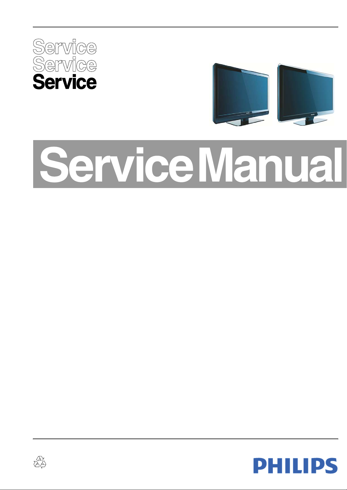
1.2.1 Rear Connections
1 & 2 - EXT1 & 2: Video RGB - In, CVBS - In/Out, Audio - In/ Out
21
20
E_06532_001.eps
2
1
050404
Figure 1-2 SCART connector
1 -Audio R 0.5 V
2 -Audio R 0.5 V
3 -Audio L 0.5 V
4 -Ground Audio Gnd H
/ 1 kohm k
RMS
/ 10 kohm j
RMS
/ 1 kohm k
RMS
5 -Ground Blue Gnd H
6 -Audio L 0.5 V
7 -Video Blue 0.7 V
/ 10 kohm j
RMS
/ 75 ohm jk
PP
8 -Function Select 0 - 2 V: INT
4.5 - 7 V: EXT 16:9
9.5 - 12 V: EXT 4:3 j
9 -Ground Green Gnd H
10 - n.c.
11 - Video Green 0.7 V
/ 75 ohm j
PP
12 - n.c.
Figure 1-1 Connection overview
13 - Ground Red Gnd H
14 - Ground P50 Gnd H
15 - Video Red 0.7 V
16 - Status/FBL 0 - 0.4 V: INT
17 - Ground Video Gnd H
18 - Ground FBL Gnd H
19 - Video CVBS/Y 1 V
20 - Video CVBS 1 V
21 - Shield Gnd H
3 - EXT3: Cinch: Video YPbPr - In, Audio - In
Gn - Video Y 1 V
Bu - Video Pb 0.7 V
Rd - Video Pr 0.7 V
Rd - Audio - R 0.5 V
Wh - Audio - L 0.5 V
4 - Cinch: S/PDIF - Out
Bk - Coaxial 0.4 - 0.6V
Service Connector (UART)
1 -Ground Gnd H
2 -UART_TX Transmit k
3 -UART_RX Receive j
5 - Cinch: Audio - Out
Rd - Audio - R 0.5 V
Wh - Audio - L 0.5 V
6 - Aerial - In
- - IEC-type (EU) Coax, 75 ohm D
I_18010_067.eps
110608
/ 75 ohm j
PP
1 - 3 V: EXT / 75 ohm j
/ 75 ohm k
PP
/ 75 ohm j
PP
/ 75 ohm jq
PP
/ 75 ohm jq
PP
/ 75 ohm jq
PP
/ 10 kohm jq
RMS
/ 10 kohm jq
RMS
/ 75 ohm kq
PP
/ 10 kohm kq
RMS
/ 10 kohm kq
RMS
Page 4
EN 4 Q522.2E LA1.
Technical Specifications, Connections, and Chassis Overview
7 - HDMI 1, 2 & 3 Digital Video, Digital Audio - In
19
18 2
1
E_06532_017.eps
250505
Figure 1-3 HDMI (type A) connector
1 -D2+ Data channel j
2-Shield Gnd H
3 -D2- Data channel j
4 -D1+ Data channel j
5-Shield Gnd H
6 -D1- Data channel j
7 -D0+ Data channel j
8-Shield Gnd H
9 -D0- Data channel j
10 - CLK+ Data channel j
11 - Shield Gnd H
12 - CLK- Data channel j
13 - n.c.
14 - n.c.
15 - DDC_SCL DDC clock j
16 - DDC_SDA DDC data jk
17 - Ground Gnd H
18 - +5V j
19 - HPD Hot Plug Detect j
20 - Ground Gnd H
8 - Mini Jack: HDMI/DVI Audio - In
Rd - Audio - R 0.5 V
Wh - Audio - L 0.5 V
/ 10 kohm jq
RMS
/ 10 kohm jq
RMS
1.2.2 Side Connections
10 - Cinch: Audio - In
Rd - Audio R 0.5 V
Wh - Audio L 0.5 V
/ 10 kohm jq
RMS
/ 10 kohm jq
RMS
11 - Cinch: Video CVBS - In
Ye - Video CVBS 1 V
/ 75 ohm jq
PP
12 - S-Video (Hosiden): Video Y/C - In
1 -Ground Y Gnd H
2 -Ground C Gnd H
3 - Video Y 1 V
4 - Video C 0.3 V
/ 75 ohm j
PP
/ 75 ohm j
PP
13 - USB2.0
1 2 3 4
E_06532_022.eps
300904
Figure 1-4 USB (type A)
1-+5V k
2 - Data (-) jk
3 - Data (+) jk
4 - Ground Gnd H
14 - HDMI: Digital Video, Digital Audio - In (see connector 7)
15 - Common Interface
68p - See diagram B09A jk
9. Head phone (Output)
Bk - Head phone 32 - 600 ohm / 10 mW ot
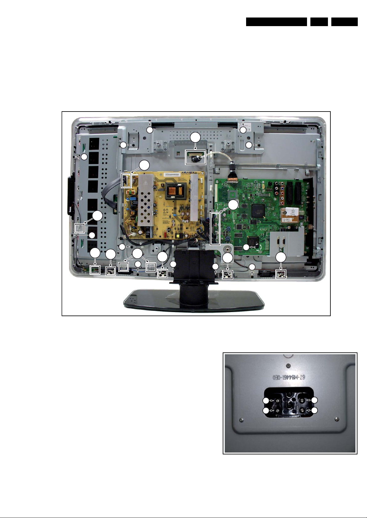
1.3 Chassis Overview
MAIN
A
SUPPLY PANEL
KEYBOARD CONTROL
E
PA NE L
IR & LED PANEL
J
Figure 1-5 PWB locations 32”
SMALL SIGNAL
BOARD
I_18010_004.eps
B
100608
Page 5
MAIN
A
SUPPLY PANEL
Technical Specifications, Connections, and Chassis Overview
EN 5Q522.2E LA 1.
KEYBOARD CONTROL
E
PANEL
IR & LED PANEL
J
MAIN
A
SUPPLY PANEL
KEYBOARD CONTROL
E
PA NE L
Figure 1-6 PWB locations 37”
SMALL SIGNAL
BOARD
I_18011_015.eps
SMALL SIGNAL
BOARD
B
240908
B
IR & LED PANEL
J
MAIN
A
SUPPLY PANEL
KEYBOARD CONTROL
E
PANEL
IR & LED PANEL
J
Figure 1-7 PWB locations 42”
Figure 1-8 PWB locations 47”
I_18010_009.eps
SMALL SIGNAL
BOARD
I_18010_064.eps
100608
B
100608
Page 6

EN 6 Q522.2E LA2.
Safety Instructions, Warnings, and Notes
2. Safety Instructions, Warnings, and Notes
Index of this chapter:
2.1 Safety Instructions
2.2 Warnings
2.3 Notes
2.1 Safety Instructions
Safety regulations require the following during a repair:
• Connect the set to the Mains/AC Power via an isolation
transformer (> 800 VA).
• Replace safety components, indicated by the symbol h,
only by components identical to the original ones. Any
other component substitution (other than original type) may
increase risk of fire or electrical shock hazard.
Safety regulations require that after a repair, the set must be
returned in its original condition. Pay in particular attention to
the following points:
• Route the wire trees correctly and fix them with the
mounted cable clamps.
• Check the insulation of the Mains/AC Power lead for
external damage.
• Check the strain relief of the Mains/AC Power cord for
proper function.
• Check the electrical DC resistance between the Mains/AC
Power plug and the secondary side (only for sets that have
a Mains/AC Power isolated power supply):
1. Unplug the Mains/AC Power cord and connect a wire
between the two pins of the Mains/AC Power plug.
2. Set the Mains/AC Power switch to the “on” position
(keep the Mains/AC Power cord unplugged!).
3. Measure the resistance value between the pins of the
Mains/AC Power plug and the metal shielding of the
tuner or the aerial connection on the set. The reading
should be between 4.5 MΩ and 12 MΩ.
4. Switch “off” the set, and remove the wire between the
two pins of the Mains/AC Power plug.
• Check the cabinet for defects, to prevent touching of any
inner parts by the customer.
2.2 Warnings
• All ICs and many other semiconductors are susceptible to
electrostatic discharges (ESD w). Careless handling
during repair can reduce life drastically. Make sure that,
during repair, you are connected with the same potential as
the mass of the set by a wristband with resistance. Keep
components and tools also at this same potential.
• Be careful during measurements in the high voltage
section.
• Never replace modules or other components while the unit
is switched “on”.
• When you align the set, use plastic rather than metal tools.
This will prevent any short circuits and the danger of a
circuit becoming unstable.
2.3 Notes
2.3.1 General
• Measure the voltages and waveforms with regard to the
chassis (= tuner) ground (H), or hot ground (I), depending
on the tested area of circuitry. The voltages and waveforms
shown in the diagrams are indicative. Measure them in the
Service Default Mode (see chapter 5) with a colour bar
signal and stereo sound (L: 3 kHz, R: 1 kHz unless stated
otherwise) and picture carrier at 475.25 MHz for PAL, or
61.25 MHz for NTSC (channel 3).
• Where necessary, measure the waveforms and voltages
with (D) and without (E) aerial signal. Measure the
voltages in the power supply section both in normal
operation (G) and in stand-by (F). These values are
indicated by means of the appropriate symbols.
2.3.2 Schematic Notes
• All resistor values are in ohms, and the value multiplier is
often used to indicate the decimal point location (e.g. 2K2
indicates 2.2 kΩ).
• Resistor values with no multiplier may be indicated with
either an “E” or an “R” (e.g. 220E or 220R indicates 220 Ω).
• All capacitor values are given in micro-farads (μ=× 10
nano-farads (n =× 10
• Capacitor values may also use the value multiplier as the
decimal point indication (e.g. 2p2 indicates 2.2 pF).
• An “asterisk” (*) indicates component usage varies. Refer
to the diversity tables for the correct values.
• The correct component values are listed in the Spare Parts
List. Therefore, always check this list when there is any
doubt.
2.3.3 BGA (Ball Grid Array) ICs
Introduction
For more information on how to handle BGA devices, visit this
URL: www.atyourservice.ce.philips.com (needs subscription,
not available for all regions). After login, select “Magazine”,
then go to “Repair downloads”. Here you will find Information
on how to deal with BGA-ICs.
BGA Temperature Profiles
For BGA-ICs, you must use the correct temperature-profile,
which is coupled to the 12NC. For an overview of these profiles,
visit the website www.atyourservice.ce.philips.com (needs
subscription, but is not available for all regions)
You will find this and more technical information within the
“Magazine”, chapter “Repair downloads”.
For additional questions please contact your local repair help
desk.
2.3.4 Lead-free Soldering
Due to lead-free technology some rules have to be respected
by the workshop during a repair:
• Use only lead-free soldering tin Philips SAC305 with order
code 0622 149 00106. If lead-free solder paste is required,
please contact the manufacturer of your soldering
equipment. In general, use of solder paste within
workshops should be avoided because paste is not easy to
store and to handle.
• Use only adequate solder tools applicable for lead-free
soldering tin. The solder tool must be able:
– To reach a solder-tip temperature of at least 400°C.
– To stabilize the adjusted temperature at the solder-tip.
– To exchange solder-tips for different applications.
• Adjust your solder tool so that a temperature of around
360°C - 380°C is reached and stabilized at the solder joint.
Heating time of the solder-joint should not exceed ~ 4 sec.
Avoid temperatures above 400°C, otherwise wear-out of
tips will increase drastically and flux-fluid will be destroyed.
To avoid wear-out of tips, switch “off” unused equipment or
reduce heat.
• Mix of lead-free soldering tin/parts with leaded soldering
tin/parts is possible but PHILIPS recommends strongly to
avoid mixed regimes. If this cannot be avoided, carefully
clear the solder-joint from old tin and re-solder with new tin.
-9
), or pico-farads (p =× 10
-12
-6
),
).
Page 7

2.3.5 Alternative BOM identification
It should be noted that on the European Service website,
“Alternative BOM” is referred to as “Design variant”.
The third digit in the serial number (example:
AG2B0335000001) indicates the number of the alternative
B.O.M. (Bill Of Materials) that has been used for producing the
specific TV set. In general, it is possible that the same TV
model on the market is produced with e.g. two different types
of displays, coming from two different suppliers. This will then
result in sets which have the same CTN (Commercial Type
Number; e.g. 28PW9515/12) but which have a different B.O.M.
number.
By looking at the third digit of the serial number, one can
identify which B.O.M. is used for the TV set he is working with.
If the third digit of the serial number contains the number “1”
(example: AG1B033500001), then the TV set has been
manufactured according to B.O.M. number 1. If the third digit is
a “2” (example: AG2B0335000001), then the set has been
produced according to B.O.M. no. 2. This is important for
ordering the correct spare parts!
For the third digit, the numbers 1...9 and the characters A...Z
can be used, so in total: 9 plus 26= 35 different B.O.M.s can be
indicated by the third digit of the serial number.
Identification: The bottom line of a type plate gives a 14-digit
serial number. Digits 1 and 2 refer to the production centre (e.g.
AG is Bruges), digit 3 refers to the B.O.M. code, digit 4 refers
to the Service version change code, digits 5 and 6 refer to the
production year, and digits 7 and 8 refer to production week (in
example below it is 2006 week 17). The 6 last digits contain the
serial number.
Directions for Use
MODEL :
PROD.NO:
32PF9968/10
AG 1A0617 000001
220-240V 50/60Hz
VHF+S+H+UHF
S
Figure 2-1 Serial number (example)
2.3.6 Board Level Repair (BLR) or Component Level Repair
(CLR)
If a board is defective, consult your repair procedure to decide
if the board has to be exchanged or if it should be repaired on
component level.
If your repair procedure says the board should be exchanged
completely, do not solder on the defective board. Otherwise, it
cannot be returned to the O.E.M. supplier for back charging!
2.3.7 Practical Service Precautions
• It makes sense to avoid exposure to electrical shock.
While some sources are expected to have a possible
dangerous impact, others of quite high potential are of
limited current and are sometimes held in less regard.
• Always respect voltages. While some may not be
dangerous in themselves, they can cause unexpected
reactions that are best avoided. Before reaching into a
powered TV set, it is best to test the high voltage insulation.
It is easy to do, and is a good service precaution.
EN 7Q522.2E LA 3.
MADE IN BELGIUM
~
128W
BJ3.0E LA
E_06532_024.eps
260308
3. Directions for Use
You can download this information from the following websites:
http://www.philips.com/support
http://www.p4c.philips.com
Page 8
EN 8 Q522.2E LA4.
Mechanical Instructions
4. Mechanical Instructions
Index of this chapter:
4.1 Cable Dressing
4.2 Service Positions
4.3 Assy/Panel Removal ME8 Styling
4.4 Assy/Panel Removal MG8 Styling
4.5 Set Re-assembly
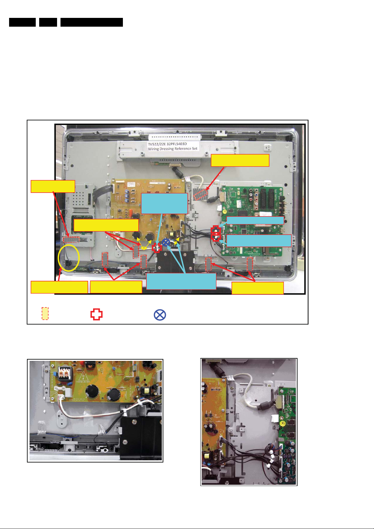
4.1 Cable Dressing
Notes:
• Figures below can deviate slightly from the actual situation,
due to the different set executions.
Tape the LVDS cable to LCD
Panel.
Tape the Control knob
cable to LCD Panel
Do not dress the control knob
cable too tight at IIR panel .
Tape the mains inlet cable to LCD
Panel away from the PSU edge
7x Tape
Tapes the terminal and IR
cable to LCD Panel
3x Saddle (M)
Saddle for mains inlet,
Speaker, Tweeter
terminal and IR cable
dressing.
Saddle for mains inlet cable dressing.
saddle position – away from PSU
area.
1x Saddle (S)
Figure 4-1 Cable dressing 32”
Saddle for speaker ferrite ring
Saddle for 8P, 11P and Speaker
cable dressing.
Tapes the terminal cables
to LCD Panel
I_18010_005.eps
110608
I_18010_006.eps
Figure 4-2 Mains inlet & left speaker cables 32”
100608
I_18010_008.eps
100608
Figure 4-3 LVDS & PSU_SSB cables 32”
Page 9
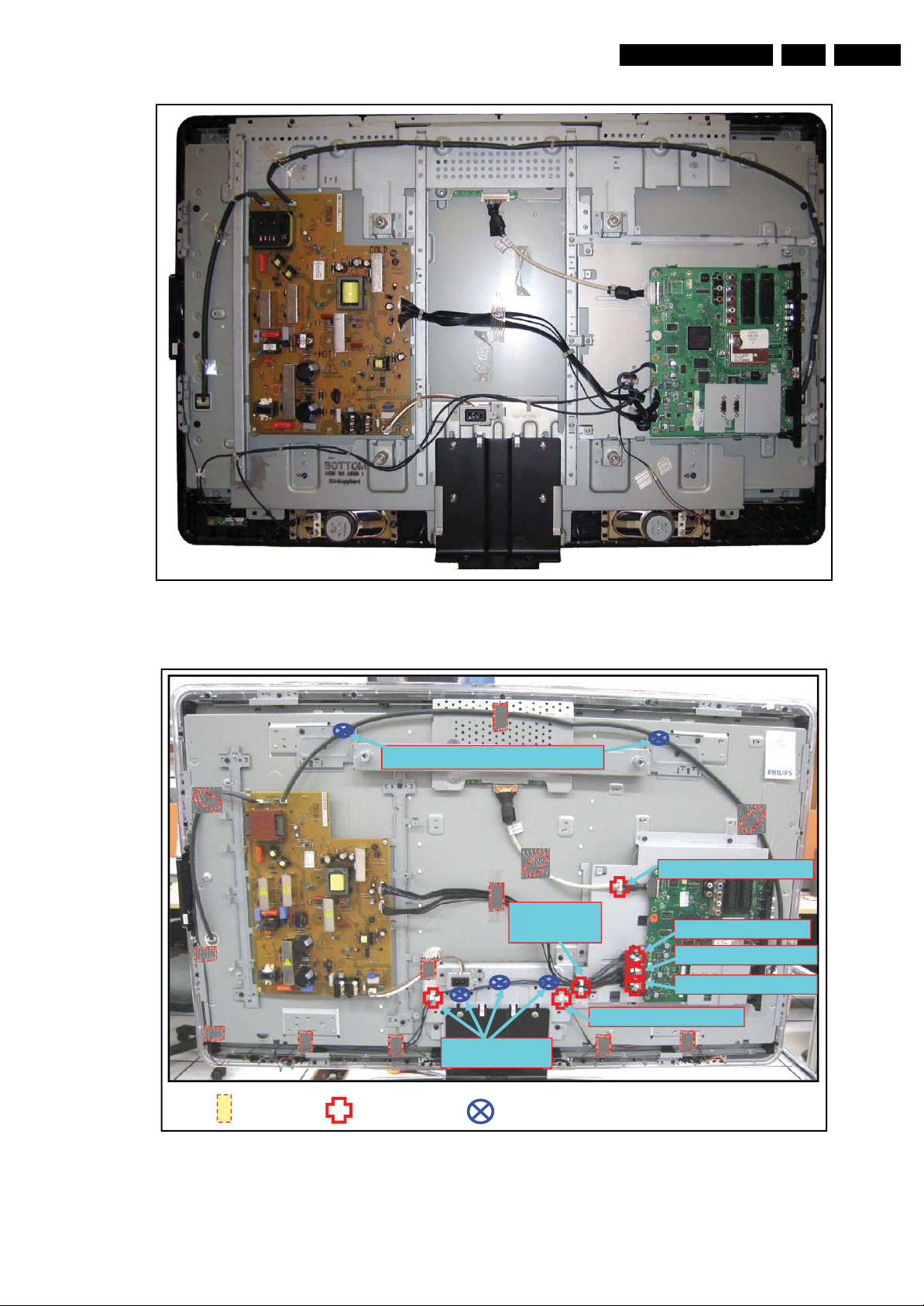
Mechanical Instructions
EN 9Q522.2E LA 4.
Figure 4-4 Cable dressing 37”
Saddles for High Voltage cable dressing
Saddle for 11P,
8P, speaker and
IR cable dressing
Saddle for LVDS cable dressing
Saddle for speaker ferrite
Saddle for 11P cable ferrite ring
Saddle for 8P cable ferrite ring
Saddle for speaker cable dressing
I_18011_016.eps
250908
12x Tape
7x Saddle (M)
Figure 4-5 Cable dressing 42”
Saddles for speaker
and IR cable dressing
5x Saddle (S)
I_18050_010.eps
100608
Page 10
EN 10 Q522.2E LA4.
Figure 4-6 Right speaker cables 42”
Mechanical Instructions
I_18010_061.eps
110608
I_18010_062.eps
Figure 4-7 Right speaker cables (with bar mounted) 42”
I_18010_063.eps
Figure 4-8 Felt and tape position for LVDS cable 42”
110608
110608
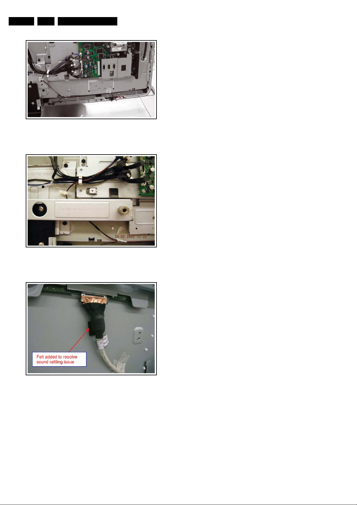
Page 11
g
Saddle for High
Voltage cable dressing
Mechanical Instructions
Saddles for High Voltage cable dressing
EN 11Q522.2E LA 4.
2x Metal bar clamp
for dressing High
Volta
e cable.
1x Metal bar clamp
for dressing
Control knob
12x Tape
Saddle for 8P/11P cable dressing
Saddles for IR,
Speaker and Mains
inlet cables dressing
9x Saddle (M)
Figure 4-9 Cable dressing 47”
Saddles for IR and
Speaker cables
dressing
8x Saddle (S)
Saddle for LVDS
dressing
Saddle for
speaker ferrite
Saddle for 11P cable ferrite ring
and Left Speaker cable dressing
Saddle for 11P cable ferrite
ring and Left Speaker cable
dressing
3x Not used
cable
ring
I_18010_065.eps
110608
I_18010_066.eps
110608
Figure 4-10 Dressing details for HV cable 47”
Page 12
EN 12 Q522.2E LA4.
Mechanical Instructions
4.2 Service Positions
For easy servicing of this set, there are a few possibilities
created:
• The buffers from the packaging.
• Foam bars (created for Service).
4.2.1 Foam Bars
1
Required for sets
1
42"
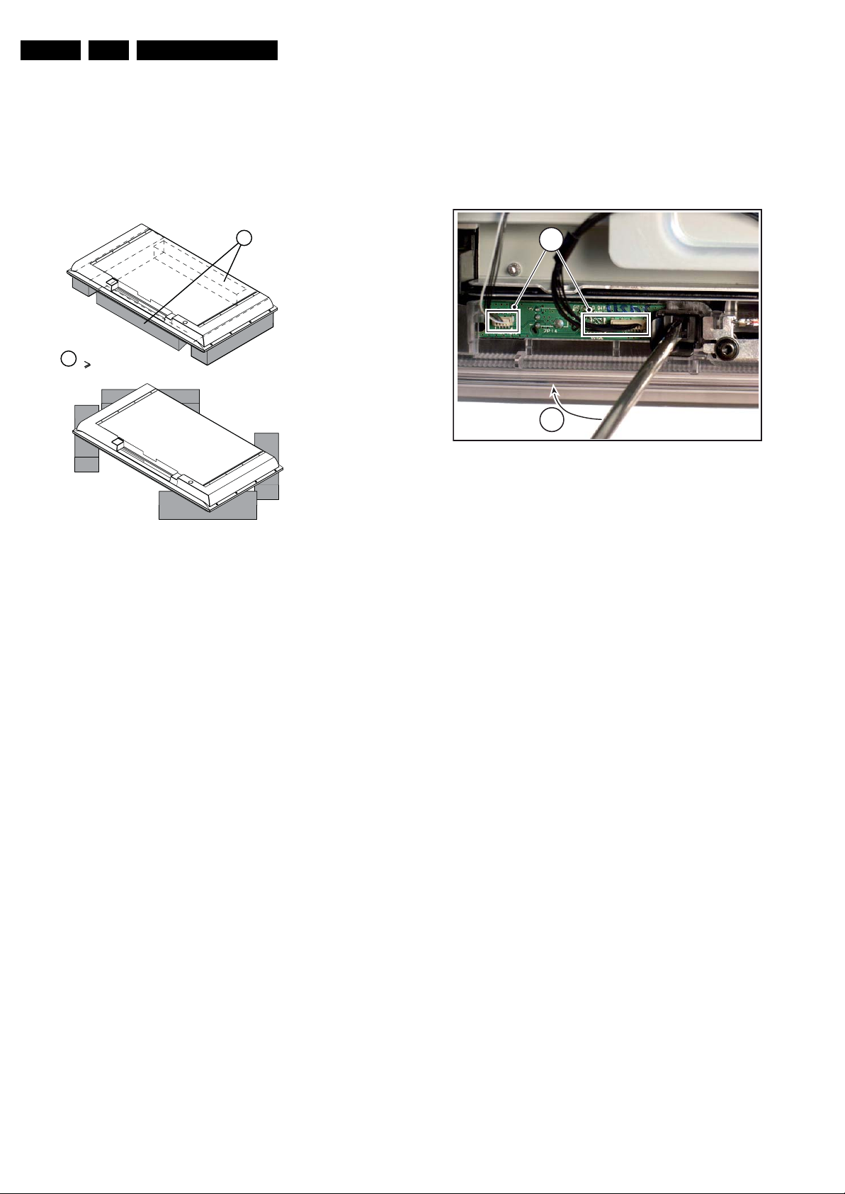
4.3.3 IR & LED Board
Refer to next figure for details.
1. Unplug connectors [1].
2. Use a flat screw driver to release the clip by pushing in the
indicated direction [2].
3. Lift the board and take it out.
When defective, replace the whole unit.
1
2
Figure 4-12 IR & LED Board
H_17650_098.eps
180108
E_06532_018.eps
171106
Figure 4-11 Foam bars
The foam bars (order code 3122 785 90580 for two pieces) can
be used for all types and sizes of Flat TVs. See figure “Foam
bars” for details. Sets with a display of 42" and larger, require
four foam bars [1]. Ensure that the foam bars are always
supporting the cabinet and never only the display.
Caution: Failure to follow these guidelines can seriously
damage the display!
By laying the TV face down on the (ESD protective) foam bars,
a stable situation is created to perform measurements and
alignments. By placing a mirror under the TV, you can monitor
the screen.
4.3 Assy/Panel Removal ME8 Styling
4.3.1 Rear Cover
Warning: Disconnect the mains power cord before you remove
the rear cover.
Note: it is not necessary to remove the stand while removing
the rear cover.
1. Remove all screws of the rear cover.
2. Lift the rear cover from the TV. Make sure that wires and
flat coils are not damaged while lifting the rear cover from
the set.
4.3.4 Key Board
1. Unplug the key board connector from the IR & LED board.
2. Remove the screws [1].
3. Lift the unit and take it out of the set.
When defective, replace the whole unit.
4.3.5 Main Supply Panel
1. Unplug all connectors.
2. Remove the fixation screws.
3. Take the board out.
When defective, replace the whole unit.
4.3.6 Small Signal Board (SSB)
Caution: It is mandatory to remount screws at their original
position during re-assembly. Failure to do so may result in
damaging the SSB.
1. Unplug the LVDS connector.
Caution: be careful, as this is a very fragile connector!
2. Unplug all other connectors.
3. Remove all screws that hold the board.
4. The SSB can now be taken out of the set, together with the
front shield and the side cover.
5. To remove the shield, remove the screws and lift it of.
6. To remove the side cover, remove the screws and pull the
cover sidewards from the SSB.
4.3.2 Speakers
Remove the screws [1] and lift the whole unit from the rear
cover. Take the speakers out together with their casing.
When defective, replace the whole unit.
Page 13
Mechanical Instructions
EN 13Q522.2E LA 4.
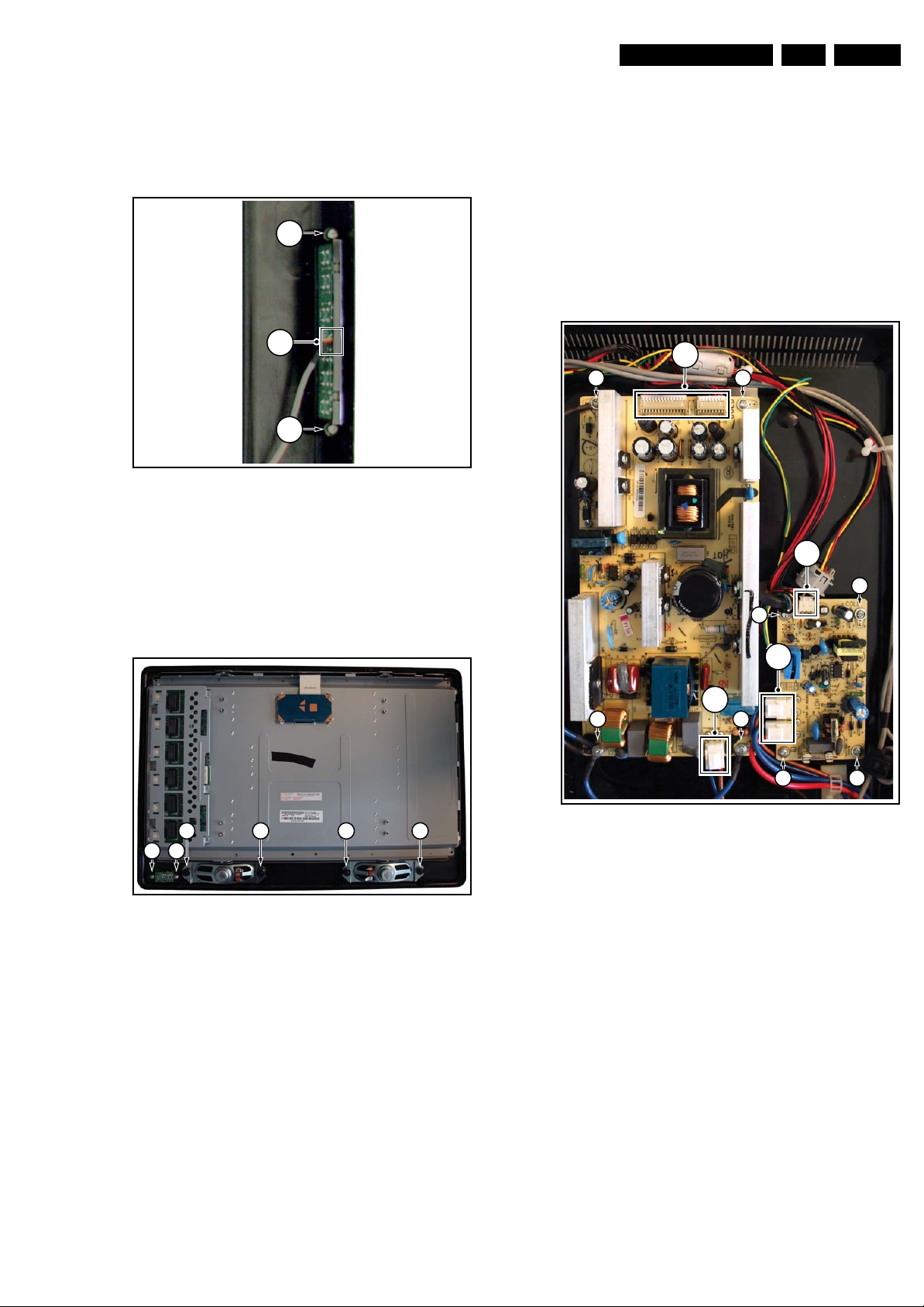
4.3.7 LCD Panel
Refer to next figure for details. As every screen size has a
(slightly) different mechanical construction (some have the
boards directly mounted on the LCD display, others use
brackets), we only describe one model. Disassembly method of
other LCD panels is similar to the one described below.
1. Unplug the LVDS connector [1].
Caution: be careful, as this is a very fragile connector!
2. Unplug the connectors [2].
3. Release the wiring tape [3].
9
7
2
3
4. Release the speaker connectors [4].
5. Remove the fixation screws from the SSB support bracket
and take the SSB out together with the bracket.
6. Do the same for the PSU.
7. Remove the fixation screws and the clamps [7].
8. Remove the fixation screws [8], that hold the subframe and
the fixation screws [9], that hold the LCD panel.
9. Lift out the sub frame.
10. The LCD panel can now be lifted from the front cabinet.
8 8
1
2
(
4x)
9
7
2
9
4
3
8
Figure 4-13 LCD Panel removal (photo from Q522.1E chassis)
4.4 Assy/Panel Removal MG8 Styling
4.4.1 Stand
1. Refer to next figure.
2. Place the TV set upside down on a table top, using the
foam bars (see section “Service Position”).
3. Remove the screws that secure the stand and remove the
stand.
9
4
8
4
8
8
4
I_17750_006.eps
250208
1
1
1
1
Figure 4-14 Stand
I_17930_040.eps
240408
Page 14
EN 14 Q522.2E LA4.
4.4.2 Rear Cover
Warning: Disconnect the mains power cord before you remove
the rear cover.
1. Refer to next figures.
2. Place the TV set upside down on a table top, using the
foam bars (see section “Service Positions”).
3. Remove the screws [1] that secure the rear cover. The
screws are located at the sides.
Be careful: Now the rear cover could be lifted but the SSB
and power supply panel(s) are mounted in the rear cover
and still connected to the LCD panel and other boards.
Those cables should be released first.
4. To release the LVDS cable lift the back cover a few
centimetres and move it downwards the set. Now unplug
the LVDS connector [2].
Caution: be careful, as this is a very fragile connector!
5. Remove the screw [3].
6. Now the rear cover can be lifted to gain access to the
speaker cables and the IR/LED panel cable. Release the
connectors [4].
1
1
1
Mechanical Instructions
1
4
4
4
I_17930_042.eps
Figure 4-17 Speaker and IR/LED panel cable release
240408
1
1 1
11
Figure 4-15 Rear cover
2
I_17930_039.eps
3
I_17930_041.eps
1
240408
240408
Figure 4-16 LVDS release
Page 15
Mechanical Instructions
EN 15Q522.2E LA 4.
4.4.3 Keyboard Control Board
1. Refer to next figure.
2. Unscrew two screws[1]
3. Unplug connector [2] and remove the board.
When defective, replace the whole unit
1
2
1
Figure 4-18 Keyboard control board
I_17930_063.eps
240408
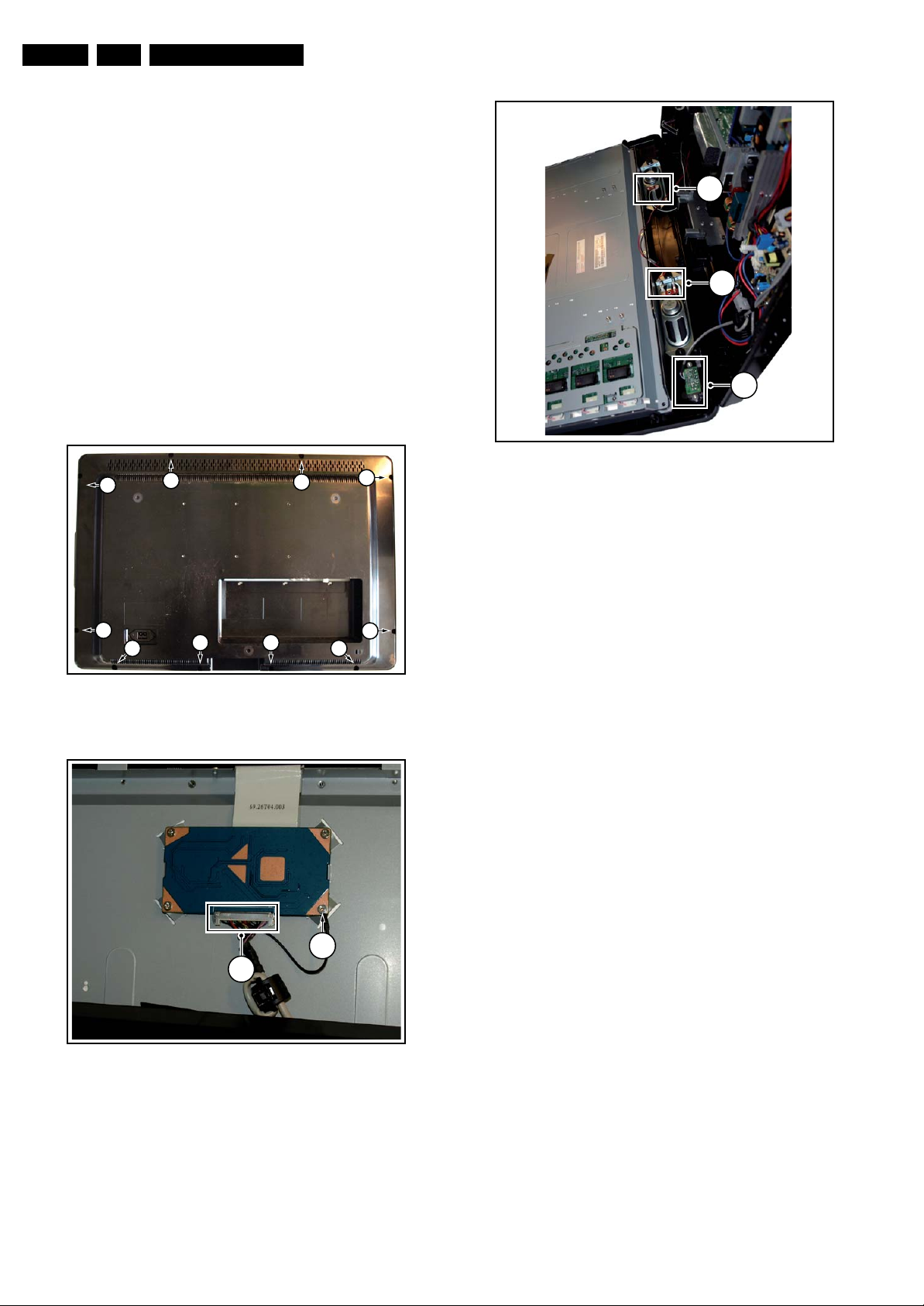
4.4.5 Power Supply Board
Due to different set executions this chassis is supplied with one
or two power supply boards and figures may differ.
Caution: it is absolutely mandatory to remount all different
screws and cables at their original position during re-assembly.
Failure to do so may result in damaging the power supply.
1. Refer to next figure.
2. Unplug all the connectors [1].
3. Remove the fixation screws [2]
4. Remove the main power supply board.
5. Unplug all the connectors [3].
6. Remove the fixation screws [4]
7. Remove the stand-by power supply board.
1
22
4.4.4 IR/LED Board and Speakers
1. Refer to next figure.
2. Remove the screws [1] and remove the IR/LED board.
3. Remove the screws [2] and remove the speakers.
When defective, replace the whole unit.
22 22
1 1
Figure 4-19 IR/LED Board and Speakers
I_17930_043.eps
240408
4
3
1
22
4 4
Figure 4-20 Power Supply Unit(s)
3
I_17930_045.eps
4
240408
Page 16
EN 16 Q522.2E LA4.
s
8
4.4.6 Inverter Board
Due to different set executions this chassis some versions are
supplied with an inverter board. Figures may differ.
1. Refer to next figure.
2. Unplug all connectors [1].
3. Release the clips [2]
4. Take out the inverter board.
Mechanical Instructions
2
4
4
4
2
3
2
1
2
Figure 4-21 Inverter Board
1
1
2
I_17930_065.eps
240408
2
Figure 4-23 SSB
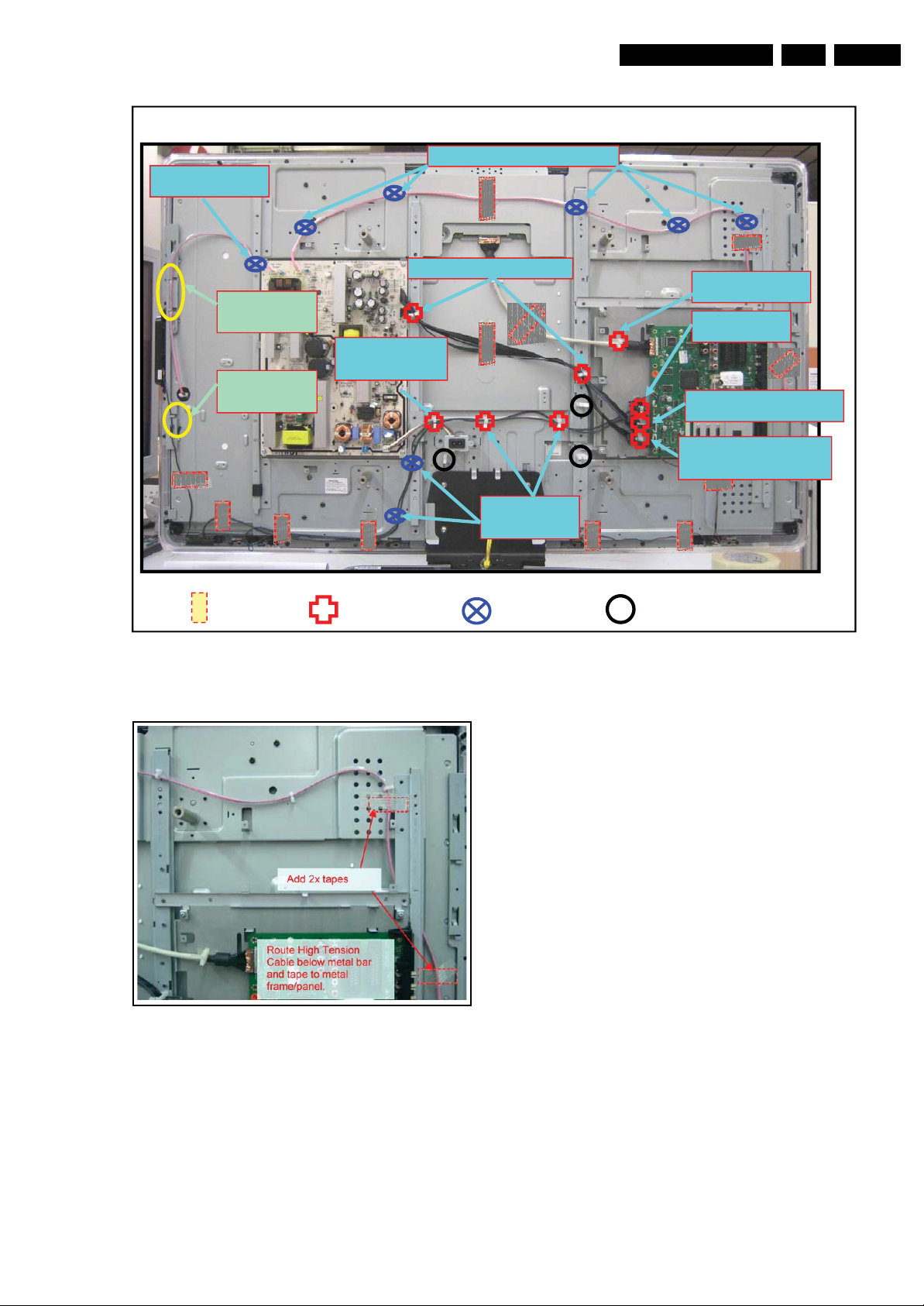
4.5 Set Re-assembly
To re-assemble the whole set, execute all processes in reverse
order.
Notes:
• While re-assembling, make sure that all cables are placed
and connected in their original position. See figure “Cable
dressing”.
• Pay special attention not to damage the EMC foams in the
set. Ensure that EMC foams are mounted correctly.
2
I_17930_048.ep
24040
4.4.7 Small Signal Board (SSB)
Caution: it is absolutely mandatory to remount all different
screws at their original position during re-assembly. Failure to
do so may result in damaging the SSB.
Removing the SSB
1. See next figures.
2. Remove the screws [1] from the SSB connector plate.
3. Remove the screws [2] from the SSB.
4. Gently lift the board from the rear cover.
5. Now unplug the LVDS connector [3].
Caution: be careful, as this is a very fragile connector!
Unplug the rest of the cables [4].
1 1
Figure 4-22 SSB connector plate
I_17930_047.eps
240408
Page 17
Service Modes, Error Codes, and Fault Finding
5. Service Modes, Error Codes, and Fault Finding
EN 17Q522.2E LA 5.
Index of this chapter:
5.1 Test Points
5.2 Service Modes
5.3 Stepwise Start-up
5.4 Service Tools
5.5 Error Codes
5.6 The Blinking LED Procedure
5.7 Protections
5.8 Fault Finding and Repair Tips
5.9 Software Upgrading
5.1 Test Points
As most signals are digital, it will be difficult to measure
waveforms with a standard oscilloscope. However, several key
ICs are capable of generating test patterns, which can be
controlled via ComPair. In this way it is possible to determine
which part is defective.
Perform measurements under the following conditions:
• Service Default Mode.
• Video: Colour bar signal.
• Audio: 3 kHz left, 1 kHz right.
5.2 Service Modes
Service Default mode (SDM) and Service Alignment Mode
(SAM) offers several features for the service technician, while
the Customer Service Mode (CSM) is used for communication
between the call centre and the customer.
This chassis also offers the option of using ComPair, a
hardware interface between a computer and the TV chassis. It
offers the abilities of structured troubleshooting, error code
reading, and software version read-out for all chassis.
(see also paragraph “ComPair”).
– Picture mute (blue mute or black mute).
– Automatic volume levelling (AVL).
– Skip/blank of non-favourite pre-sets.
How to Activate SDM
For this chassis there are two kinds of SDM: an analogue SDM
and a digital SDM. Tuning will happen according table “SDM
Default Settings”.
• Analogue SDM: use the standard RC-transmitter and key
in the code “062596”, directly followed by the “MENU”
button.
Note: It is possible that, together with the SDM, the main
menu will appear. To ;switch it “off”, push the “MENU”
button again.
• Digital SDM: use the standard RC-transmitter and key in
the code “062593”, directly followed by the “MENU” button.
Note: It is possible that, together with the SDM, the main
menu will appear. To switch it “off”, push the “MENU”
button again.
• Analogue SDM can also be activated by shorting for a
moment the two solder pads [1] (see figure “Service mode
pads”) on the SSB, with the indication “SDM”. Activation
can be performed in all modes, except when the set has a
problem with the Stand-by Processor.
1
1
SDM
SDM
SDMSPI
12
5.2.1 Service Default Mode (SDM)
Purpose
• To create a pre-defined setting, to get the same
measurement results as given in this manual.
• To override SW protections detected by stand-by
processor and make the TV start up to the step just before
protection (a sort of automatic stepwise start up). See
paragraph “Stepwise Start Up”.
• To override SW protections detected by MIPS. See also
paragraph “Error codes”.
• To start the blinking LED procedure (not valid for
protections detected by stand-by software).
Specifications
Table 5-1 SDM default settings
Region Freq. (MHz)
Europe, AP(PAL/Multi) 475.25 PAL B/G
Europe, AP DVB-T 546.00 PID
Video: 0B 06 PID
PCR: 0B 06 PID
Audio: 0B 07
• All picture settings at 50% (brightness, colour, contrast).
• All sound settings at 50%, except volume at 25%.
• All service-unfriendly modes (if present) are disabled, like:
– (Sleep) timer.
– Child/parental lock.
Default
system
DVB-T
I_18010_068.eps
Figure 5-1 Service mode pads
After activating this mode, “SDM” will appear in the upper right
corner of the screen (if you have picture).
How to Navigate
When you press the “MENU” button on the RC transmitter, the
set will toggle between the SDM and the normal user menu
(with the SDM mode still active in the background).
How to Exit SDM
Use one of the following methods:
• Switch the set to STAND-BY via the RC-transmitter.
• Via a standard customer RC-transmitter: key in “00”sequence.
5.2.2 Service Alignment Mode (SAM)
Purpose
• To perform (software) alignments.
• To change option settings.
• To easily identify the used software version.
• To view operation hours.
• To display (or clear) the error code buffer.
130608
Page 18
EN 18 Q522.2E LA5.
Service Modes, Error Codes, and Fault Finding
How to Activate SAM
Via a standard RC transmitter: key in the code “062596”
directly followed by the “INFO” button. After activating SAM
with this method a service warning will appear on the screen,
you can continue by pressing the red button on the RC.
Contents of SAM:
• Hardware Info.
– A. SW Version. Displays the software version of the
main software (example: Q522E-1.2.3.4 =
AAAAB_X.Y.W.Z).
• AAAA= the chassis name.
• B= the region: A= AP, E= EU, L= LatAm, U = US.
For AP sets it is possible that the Europe software
version is used.
• X.Y.W.Z= the software version, where X is the
main version number (different numbers are not
compatible with one another) and Y.W.Z is the sub
version number (a higher number is always
compatible with a lower number).
– B. SBY PROC Version. Displays the software version
of the stand-by processor.
– C. Production Code. Displays the production code of
the TV, this is the serial number as printed on the back
of the TV set. Note that if an NVM is replaced or is
initialized after corruption, this production code has to
be re-written to NVM. ComPair will foresee in a
possibility to do this.
• Operation Hours. Displays the accumulated total of
operation hours (not the stand-by hours). Every time the
TV is switched “on/off”, 0.5 hours is added to this number.
• Errors (followed by maximal 10 errors). The most recent
error is displayed at the upper left (for an error explanation
see paragraph “Error Codes”).
• Reset Error Buffer. When you press “cursor right” (or the
“OK button) and then the “OK” button, the error buffer is
reset.
• Alignments. This will activate the “ALIGNMENTS” submenu.
• Dealer Options. Extra features for the dealers.
• Options. Extra features for Service. For more info
regarding option codes, see chapter 8 “Alignments”.
Note that if you change the option code numbers, you have
to confirm your changes with the “OK” button before you
store the options. Otherwise you will loose your changes.
• Initialise NVM. The moment the processor recognizes a
corrupted NVM, the “initialize NVM” line will be highlighted.
Now, you can do two things (dependent of the service
instructions at that moment):
– Save the content of the NVM via ComPair for
development analysis, before initializing. This will give
the Service department an extra possibility for
diagnosis (e.g. when Development asks for this).
– Initialize the NVM.
Note: When you have a corrupted NVM, or you have replaced
the NVM, there is a high possibility that you will not have picture
anymore because your display code is not correct. So, before
you can initialize your NVM via the SAM, you need to have a
picture and therefore you need the correct display option. Refer
to chapter 8 for details. To adapt this option, you can use
ComPair (the correct HEX values for the options can be found
in chapter 8 “Alignments”) or a method via a standard RC
(described below).
Changing the display option via a standard RC: Key in the
code “062598” directly followed by the “MENU” button and
“XXX”, where XXX is the 3 digit decimal display code (see table
“Option code overview” in chapter 8 “Alignments”, or sticker on
the side/bottom of the cabinet). Make sure to key in all three
digits, also the leading zero’s. If the above action is successful,
the front LED will go out as an indication that the RC sequence
was correct. After the display option is changed in the NVM, the
TV will go to the Stand-by mode. If the NVM was corrupted or
empty before this action, it will be initialized first (loaded with
default values). This initializing can take up to 20 seconds.
Display Option
Code
39mm
040
PHILIPS
MODEL:
32PF9968/10
27mm
PROD.SERIAL NO:
AG 1A0620 000001
(CTN Sticker)
E_06532_038.eps
240108
Figure 5-2 Location of Display Option Code sticker
• Store. All options and alignments are stored when
pressing “cursor right” (or the “OK” button) and then the
“OK”-button.
• SW Maintenance.
– SW Events. Not useful for Service purposes. In case
of specific software problems, the development
department can ask for this info.
– HW Events. Not useful for Service purposes. In case
of specific software problems, the development
department can ask for this info.
• Test settings. For development purposes only.
• Upload to USB. To upload several settings from the TV to
a USB stick, which is connected to the Side I/O. The items
are “Channel list”, “Personal settings”, “Option codes”,
“Display-related alignments” and “History list”. First you
have to create a directory “repair” in the root of the USB
stick.To upload the settings you have to select each item
separately, press “cursor right” (or the “OK button), confirm
with “OK” and wait until “Done” appears. In case the
download to the USB stick was not successful “Failure” will
appear. In this case, check if the USB stick is connected
properly and if the directory “repair” is present in the root of
the USB stick. Now the settings are stored onto your USB
stick and can be used to download onto another TV or
other SSB. Uploading is of course only possible if the
software is running and if you have a picture. This method
is created to be able to save the customer’s TV settings
and to store them into another SSB.
• Download from USB. To download several settings from
the USB stick to the TV. Same way of working as with
uploading. To make sure that the download of the channel
list from USB to the TV is executed properly, it is necessary
to restart the TV and tune to a valid preset if necessary.
Note: The “History list item” can not be downloaded from
USB to the TV. This is a “read-only” item. In case of specific
problems, the development department can ask for this
info.
How to Navigate
• In SAM, you can select the menu items with the “CURSOR
UP/DOWN” key on the RC-transmitter. The selected item
will be highlighted. When not all menu items fit on the
screen, move the “CURSOR UP/DOWN” key to display the
next/previous menu items.
• With the “CURSOR LEFT/RIGHT” keys, it is possible to:
– (De) activate the selected menu item.
– (De) activate the selected sub menu.
• With the “OK” key, it is possible to activate the selected
action.
How to Exit SAM
Use one of the following methods:
• Press the “MENU” button on the RC-transmitter.
• Switch the set to STAND-BY via the RC-transmitter.
Page 19

Service Modes, Error Codes, and Fault Finding
EN 19Q522.2E LA 5.
5.2.3 Customer Service Mode (CSM)
Purpose
When a customer is having problems with his TV-set, he can
call his dealer or the Customer Help desk. The service
technician can then ask the customer to activate the CSM, in
order to identify the status of the set. Now, the service
technician can judge the severity of the complaint. In many
cases, he can advise the customer how to solve the problem,
or he can decide if it is necessary to visit the customer.
The CSM is a read only mode; therefore, modifications in this
mode are not possible.
When in this chassis CSM is activated, a colour bar test pattern
will be visible for 5 seconds. This test pattern is generated by
the Pacific3. So if you see this test pattern you can determine
that the back end video chain (Pacific3, LVDS, and display) of
the SSB is working. In case of a set with DFI panel, an extra
test picture is generated. So you will see the Pacific3 test
picture for 3 seconds and then the DFI EPLD test picture for
another 3 seconds. With this extra test picture you can
determine if the DFI board is working properly.
Also new in this chassis: when you activate CSM and there is
a USB stick connected to the TV, the software will dump the
complete CSM content to the USB stick. The file (Csm.txt) will
be saved in the root of your USB stick. This info can be handy
if you do not have picture.
Another new item in this chassis is when CSM is activated, the
complete error-buffer content will be shown via the blinking
LED procedure.
How to Activate CSM
Key in the code “123654” via the standard RC transmitter.
Note: Activation of the CSM is only possible if there is no (user)
menu on the screen!
How to Navigate
By means of the “CURSOR-DOWN/UP” knob on the RCtransmitter, you can navigate through the menus.
Contents of CSM
• Set Type. This information is very helpful for a help desk/
workshop as reference for further diagnosis. In this way, it
is not necessary for the customer to look at the rear of the
TV-set. Note that if an NVM is replaced or is initialized after
corruption, this set type has to be re-written to NVM.
ComPair will foresee in a possibility to do this.
• Production Code. Displays the production code (the serial
number) of the TV. Note that if an NVM is replaced or is
initialized after corruption, this production code has to be
re-written to NVM. ComPair will foresee a in possibility to
do this.
• Code 1. Gives the last five errors of the error buffer. As
soon as the built-in diagnose software has detected an
error, the buffer is adapted. The last occurred error is
displayed on the leftmost position. Each error code is
displayed as a 2-digit number. When less than 10 errors
occur, the rest of the buffer is empty (00). See also
paragraph “Error Codes” for a description.
• Code 2. Gives the first five errors of the error buffer. See
also paragraph “Error Codes” for a description.
• Options 1. Gives the option codes of option group 1 as set
in SAM (Service Alignment Mode).
• Options 2. Gives the option codes of option group 2 as set
in SAM (Service Alignment Mode).
• 12NC SSB. Gives an identification of the SSB as stored in
NVM. Note that if an NVM is replaced or is initialized after
corruption, this identification number has to be re-written to
NVM. ComPair will foresee in a possibility to do this. This
identification number consists of 14 characters and is built
up as follows:
- Seven last characters of the 12NC of the SSB itself.
- the serial number of the SSB, which consists of seven
digits. Both can be found on a sticker on the PWB of the
SSB itself. The format of the identification number is then
as follows: <last seven characters of 12NC of SSB><serial
number of SSB> (total fourteen characters).
• Installed date. Indicates the date of the first installation of
the TV. This date is acquired via time extraction.
• Digital Natural Motion. Gives the status of the Digital
Natural Motion setting as set by the customer. Remark: a
customer can choose between “OFF”, “MINIMUM” and
“MAXIMUM”, but in CSM this item will only show “OFF” or
“ON” (“ON” in case the customer has chosen “MINIMUM”
or “MAXIMUM”)
• Pixel Plus. Gives the last status of the Perfect Pixel HD
setting, as set by the customer. Possible values are “ON”
and “OFF”. See DFU on how to change this item.
• DNR. Gives the last status of the Noise reduction setting,
as set by the customer. Possible values are “OFF”,
“MINIMUM”, “MEDIUM” and “MAXIMUM”. See DFU on
how to change this item.
• Noise Figure. Gives an indication of the signal quality for
the selected transmitter. Possible values are “BAD”,
“AVERAGE”, “GOOD“ and “DIGITAL”. In case of a digital
channel, this item will never indicate: “BAD”, “GOOD” or
“AVERAGE” but only displays “DIGITAL”.
• 12NC Display. Shows the 12NC of the display.
• Head phone Volume. Gives the last status of the head
phone volume, as set by the customer. The value can vary
from 0 (volume is minimum) to 100 (volume is maximum).
See DFU on how to change this item.
• Surround Mode. Indicates the by the customer selected
sound mode (or automatically chosen mode). Possible
values are “STEREO” and “VIRTUAL DOLBY
SURROUND”. It can also have been selected
automatically by signalling bits (internal software). See
DFU on how to change this item.
• AVL. Indicates the last status of AVL (Automatic Volume
Level) as set by the customer: See DFU on how to change
this item.
• Delta Volume. Indicates the last status of the delta volume
for the selected preset as set by the customer: from “-12”
to “+12”. See DFU on how to change this item.
• Volume. Indicates the last status of the volume for the
selected preset as set by the customer: from “0” to “100”.
See DFU on how to change this item.
• Balance. Indicates the last status of the balance for the
selected preset as set by the customer: from “-10” to “+10”.
See DFU on how to change this item.
• Preset Lock. Indicates if the selected preset has a child
lock: “LOCKED” or “UNLOCKED”. See DFU on how to
change this item.
• Child Lock. Indicates the status of the Child lock. See DFU
on how to change this item.
• Lock After. Indicates at what time the channel lock is set:
“OFF” or e.g. “18:45” (lock time). See DFU on how to
change this item.
• Parental Rating Lock. Indicates the “Parental rating” as
set by the customer. See DFU on how to change this item.
• Parental Rating Status. Indicates the “Parental rating” as
transmitted by the broadcaster (if applicable). If the
parental rating status is indicating a higher age then the
parental rating lock as set by the customer, you will need to
enter the child lock code.
• TV Ratings Lock. Only applicable for US.
• Movie Ratings Lock. Only applicable for US.
• On timer. Indicates if the “On timer” is set “ON” or “OFF”
and when it is set to “ON”, also start time, start day and
program number is displayed. See DFU on how to change
this item.
• Location. Gives the last status of the location setting as
set via the installation menu. Possible values are “SHOP”
and “HOME”. If the location is set to “SHOP”, several
settings are fixed. So for a customer location must be set
to “HOME”. Can be changed via the installation menu (see
also DFU).
• HDMI Key Validity. Indicates if the HDMI keys (or HDCP
keys) are valid or not. In case these keys are not valid and
Page 20
EN 20 Q522.2E LA5.
Service Modes, Error Codes, and Fault Finding
the customer wants to make use of the HDMI functionality,
the SSB has to be replaced.
• Tuner Frequency. Indicates the frequency the transmitter
is tuned to.
• TV System. Gives information about the video system of
the selected transmitter. In case a DVBT signal is received
this item will also show ATSC.
– BG: PAL BG signal received
– DK: PAL DK signal received
– L/La: SECAM L/La signal received
– I: PAL I signal received
– M: NTSC M signal received
– ATSC: ATSC signal received
– DVB: DVBT signal received
• 12NC One Zip SW. Displays the 12NC number of the onezip file as it is used for programming software in production.
In this one-zip file all below software versions can be found.
• Initial Main SW. Displays the main software version which
was initially loaded by the factory.
• Current Main SW. Displays the built-in main software
version. In case of field problems related to software,
software can be upgraded. As this software is consumer
upgradable, it will also be published on the Internet.
Example: Q582E_1.2.3.4.
• Flash Utils SW. Displays the software version of the
software which contains all necessary components of the
download application. To program this software, EJTAG
tooling is needed. Example: Q582E_1.2.3.4.
• Stand-by SW. Displays the built-in stand-by processor
software version. Upgrading this software will be possible
via ComPair or via USB (see chapter Software upgrade).
Example: STDBY_3.0.1.2.
• MOP SW. Only applicable for US. At the time of release of
this manual, there was still a problem with this item, and
some rubbish was displayed. Ignore this.
• Pacific 3 Flash SW (if applicable). Displays the Pacific 3
software version.
• NVM Version. Displays the NVM version as programmed
by factory.
• Display Parameters. for development purposes only.
• Private PQ Parameters. for development purposes only.
• Public PQ Parameters. for development purposes only.
• Ambilight Parameters. for development purposes only.
• Acoustics Parameters. for development purposes only.
• DFI Software (if applicable). Displays the DFI EPLD
software.
• DFI Ambilight software (if applicable). Displays the DFI
ambilight EPLD software.
How to Exit CSM
Press “MENU” on the RC-transmitter.
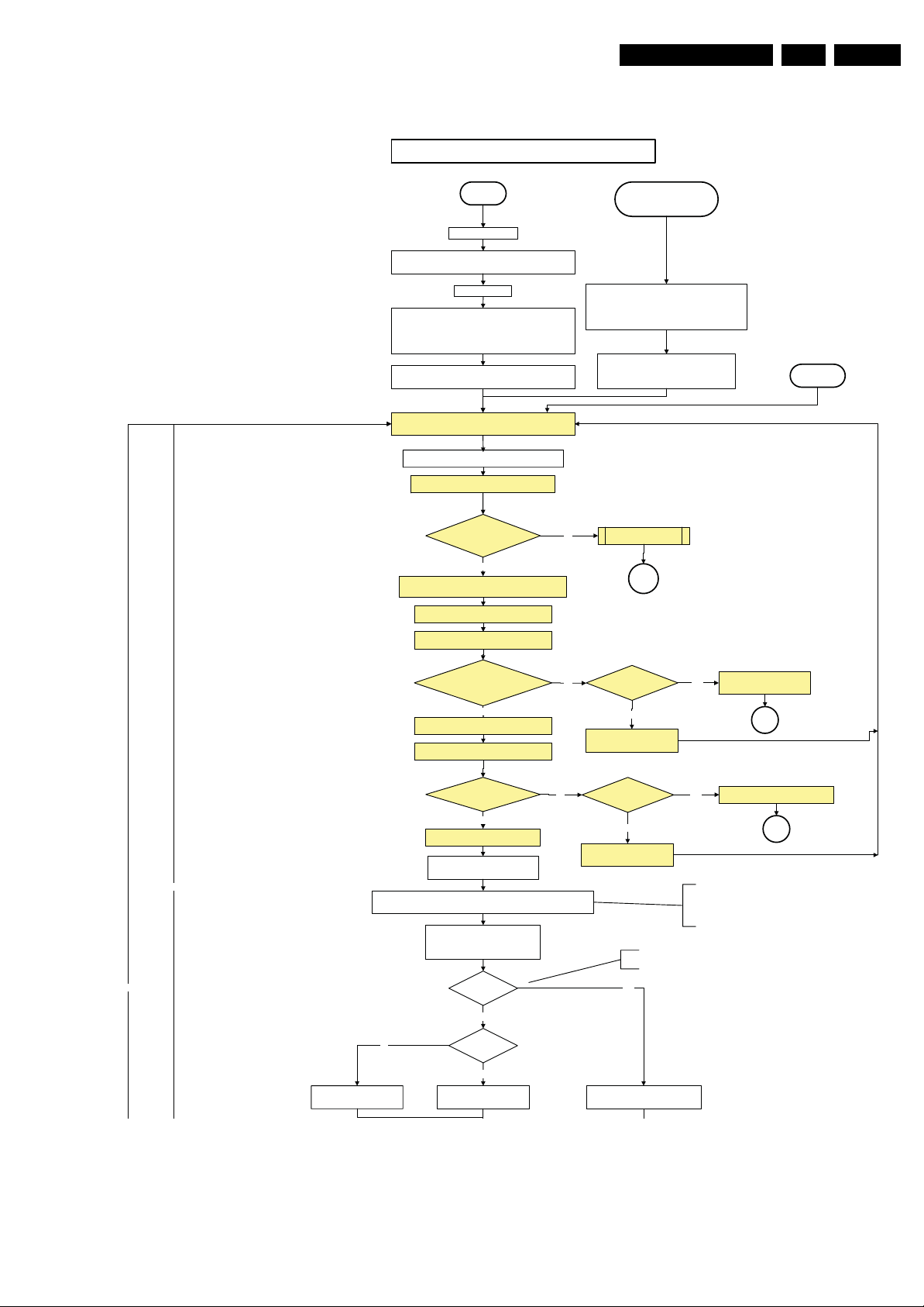
5.3 Stepwise Start-up
There are two possible situations: one for protections detected
by the stand-by software and one for protections detected by
the main software.
When the TV is in a protection state due to an error detected by
stand-by software (and thus blinking an error) and SDM is
activated via short-circuiting the pins on the SSB, the TV starts
up until it reaches the situation just before protection. So, this
is a kind of automatic stepwise start-up. In combination with the
start-up diagrams below, you can see which supplies are
present at a certain moment. Important to know is, that if e.g.
the 3V3 detection fails (and thus error 8 is blinking) and the TV
is restarted via SDM, the Stand-by Processor will enable the
3V3, but will not go to protection now. The TV will stay in this
situation until it is reset (Mains/AC Power supply interrupted).
Caution: in case the start up in this mode with a faulty FET
7U08 is done, you can destroy all ICs supplied by the +3V3,
due to overvoltage. It is recommended to measure first the FET
7U08 on short-circuit before activating SDM via the service
pads.
When the TV is in protection state due to an error detected by
main software (MIPS protection) and SDM is activated via
short-cutting the service pads on the SSB, the TV starts up and
ignores the error.
In this chassis, only error “63” (power-ok) is a MIPS protection
and already displays the failure via blinking LED.
The abbreviations “SP” and “MP” in the figures stand for:
• SP: protection or error detected by the Stand-by
Processor.
• MP: protection or error detected by the MIPS Main
Processor.
Off
Mains
off
- WakeUp requested
- Acquisition needed
- No data Acquisition
required
- Tact SW pushed
- Last status is hibernate
after mains ON
Tact sw itch
pushed
- Tact sw itch pushed
- last status is hibernate
after mains ON
St by
Hibernate
On
The Protect ion state and t he Hibernate state are hard ware wise
identical to the Standby st ate but have oth er , more limited wake up reasons.
Figure 5-3 Transition diagram
Mains
on
Semi
St by
GoToProtection
WakeUp
requested
- St by requested
- Tact SW pushed
WakeUp
requested
(SDM)
Protection
Active
GoToProtection
I_18010_077.eps
110608
Page 21
Service Modes, Error Codes, and Fault Finding
Off/Stby to Semi
EN 21Q522.2E LA 5.
Off
Mains is app lied
Standby Supply starts running.
All standby supply voltages become available .
st-by µ P resets
All I/O lines have a High default state:
- Switch PNX8541 in reset (active LOW).
- Keep the Audio-reset high.
- NVM p ower line is h igh, no NVM co mmunication p ossible.
Initialise I/O pins of the st-by µP, start keyboard scanning, RC
detection. Wake up reasons are off.
Switch ON PSU supply by switching LOW the Standby I/O
Wait 50m s and then star t polling th e DETECT 2
line.
+12V is switched on
every 40ms.
2900 ms
Yes
activate DETECT 2 algorithm
Enable the supply for
+3V3 an d +5V (ENABLE- 3V3)
Start polling the detect 1
every 40ms
Stand by or
Protection
If the protection state was left by short circuiting the
SDM pins, detection of a protection condition during
startup will stall the startup. Protection conditions in a
playing set will be ignor ed. Th e protectio n mode will
No
not be entered.
- Switch Audio-Reset high.
It is low in the standby mode if the standby
mode lasted longer than 10s.
12V supply” error 6DETECT 2 received within
SP
Restart
DETECT 1 = High
within
250 ms after enable-3V3 toggle?
Yes
Activate DETECT 1 algorithms
Wait 20ms
SUPPLY-F AULT I/O line
is High ?
Yes
Enable the supply fault detection
algorithm
Set I²C slave address
No
No
Release AVC system reset
Feed warm boot script
Switch LOW the RESET-NVM_WP-NANDFLASH line. Add a 2ms delay
before trying to address the NVM to allow correct NVM initialization.
No
of Standby µP to (A0h)
Detect EJTAG debug probe
(pulling pin of the probe interface to
ground by inserting EJTAG probe)
EJTAG probe
connected ?
No
Cold boot?
Yes
Relea se AVC system r eset
Feed cold boot script
No
Standby line set to HIGH for 5
No
Detect 1 = High?
Standby line set to HIGH for 5
No
seconds
Yes
No
seconds
This will allow access to NVM and
NAND FLASH and can not be done
earlier because the FLASH needs to
be in Write Protect as long as the
supplies are not available.
An EJTAG probe (e.g. WindPower ICE probe) can
be connected for Linux Kernel debugging purposes.
Yes
Release AVC system reset
Feed initializing boot script
disable alive mechanism
Voltage output error: 8Supply Fault = High? Yes
SP
Supply fault error 9
SP
I_18010_069a.eps
110608
Figure 5-4 “Off” to “Semi Stand-by” flowchart (part 1)
Page 22
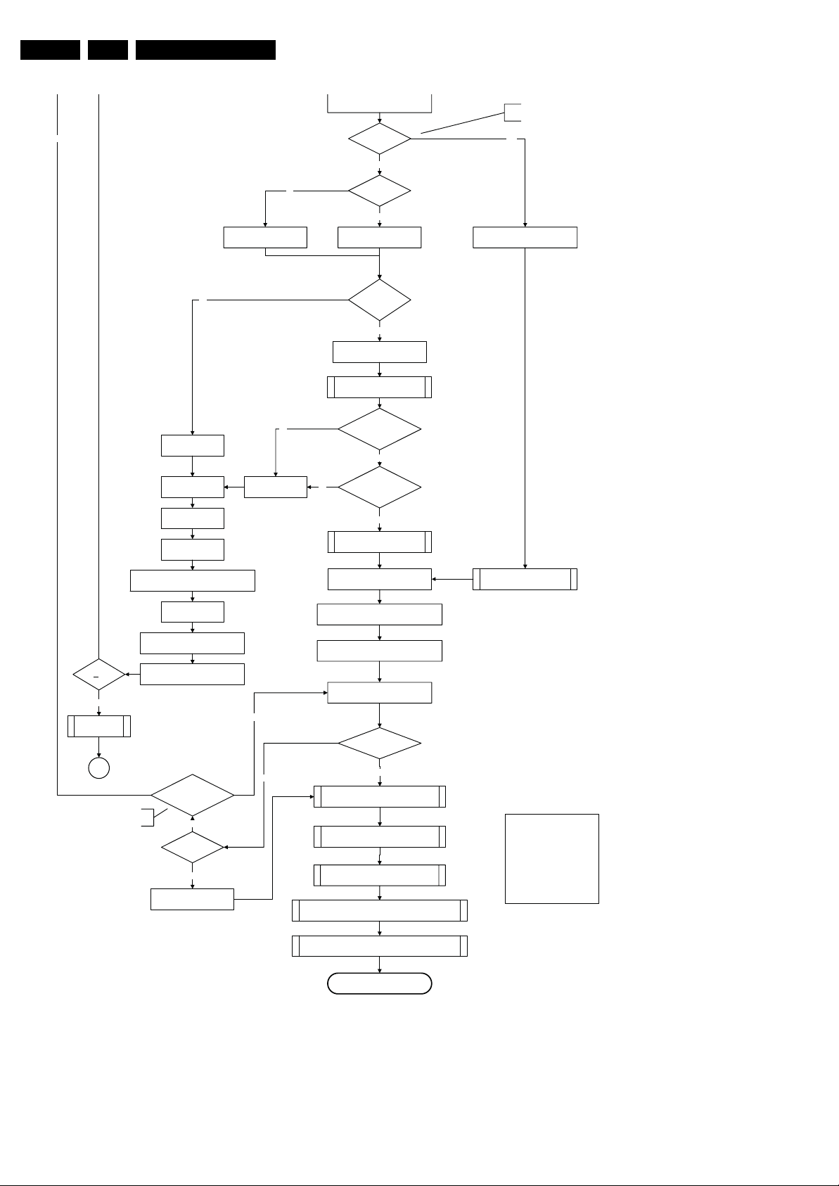
EN 22 Q522.2E LA5.
(pulli
No
Service Modes, Error Codes, and Fault Finding
ng pin of the probe interface to
ground by inserting EJTAG probe)
EJTAG probe
connected ?
No
An EJTAG probe (e.g. WindPower ICE probe) can
be connected for Linux Kernel debugging purposes.
Yes
Release AVC system reset
Feed warm boot script
No
Code = 5
Switch AVC PNX85 41
in reset (active lo w)
Wait 10ms
Switch t he NVM re set
line HIGH .
Disable all supply related protections and
switch off the +2V5, +3V3 DC/DC converter.
Code = 53
No
No
No
Cold boot?
Yes
Relea se AVC system r eset
Feed cold boot script
Bootscript ready
in 1250 ms?
Yes
Set I²C slave address
of Standby µP to (60h)
RPC start (comm. protocol)
Flash to RAM image
tran sfer succee ded
within 30s?
Yes
SW initializat ion
succeede d
within 20s?
Yes
Enable Alive check mechanism
MIPS reads the wake up reason
from standby µP.
Release AVC system r eset
Feed initializing boot script
disable alive mechanism
Wait until AVC starts to
commun icate
3-th try?
Yes
Blink Code as
error code
SP
No
- Channeldecoder type TDA10048
can be reloaded without reset.
Wait 5ms
switch of f the rema ining DC/DC
conver ters
Switch Standby
I/O line high.
Channel decoder
TDA 10048?
No
Third try?
Yes
Log channel decoder error
Start 4 seconds preheating timer in case of
an LPL scanning backlight LCD set.
Initialize a udio
Download firmware into the channel
decoder
Yes
Downloaded
successfull y?
No
Initialize tuner , Master IF and chan nel
Wait until Cpipe delivers a stable output
Initialize AutoTV by tr iggering CHS AutoT V Init inter face
Do not enter Semi-- Standby state in case of an LPL
scanning backlight LCD set before 4s preheating timer has
elapsed.
Yes
decoder
Initialize source selectio n
clock
Semi-Standby
Import ant remark :
Input v ertical frequency
changes (48 /50/60H z)
detect ed during startup
sequence should not be
taken int o account . The
end situat ion should
alway s be safeguarded .
.
I_18010_069b.eps
110608
Figure 5-5 “Off” to “Semi Stand-by” flowchart (part 2)
Page 23
Service Modes, Error Codes, and Fault Finding
Constraints taken into account:
- Display may only be started when valid LVDS output clock can be delivered by the AVC .
- Between 5 and 50 ms after power is supplied, display should receive valid LVDS clock.
- Backlight Control PWM output should always keep low until LVDS power is supplied .
- Minimum wait time to switch “on” the lamp after power up is 200ms.
- To have a reliable operation of the backlight, the backlight should be driven with a PWM duty cycle of 100%
during the first 2 seconds. Only after this first 2 seconds, the PWM may be set to the required output level (Note
that the PWM output should be present before the backlight is switched on). To minimize the artefacts, the picture
should only be unblanked after this first second.
EN 23Q522.2E LA 5.
action holder: AVC
action holder: St-by
autonomous action
The assumption h ere is that a fast toggle (<2s)
can only happen during ON->SEMI ->ON. In
these states, the AVC is still active and can
provide t he 2s delay. If the t ransition ON-> SEMI>STBY->SEMI->ON can be made in less than 2s,
we have to delay t he semi -> stby transition until
CPipe already generates a valid output
clock in t he semi -standby state: displa y
startup can start immediately when leaving
the semi-standby state.
the requ irement is met.
Rewrite Pacific register 0x03 (output format) with TcuUpdate:
this command is sometimes not processed properly by the
Pacific at initialisation time , resending it here solves the issue.
Switch on the display by switching CTRL1- MIPS_LCD-
Switch off the dimming backlight feature and
Semi Standby
Wait until previous on-state is left more than 2
seconds ago. (to prevent LCD display problems)
Assert RGB video blanking
and audio mute
PWR-ON to low.
Enable Backlight Control PWM output
wait 250ms (m in. = 200ms)
make sure PWM output is set to 100%
Initialize audio and video
processing IC's and functions
according needed use case.
Switch “on” LCD backlight
The higher level requirement is that
audio and video should be demuted
without transient effects and that the
audio should be demuted maximum 1s
before or at the same time as the
unblanking of the video.
Figure 5-6 “Semi Stand-by” to “Active” flowchart (non-DFI)
Wait until valid and stable audio and video, corr esponding to
the requested output is delivered by the AVC AND the
backlight PWM has been on for 2 seconds.
Switch Audio -Reset low and wait 5ms
Release audio mute and wait 100ms before any other audio
handling is done (e.g. volume change).
Restore dimming backlight feature, PWM output and unblank
the video.
Active
I_18010_070.eps
110608
Page 24
EN 24 Q522.2E LA5.
Service Modes, Error Codes, and Fault Finding
Active
Mute all sound outputs via softmute
Wait 100ms
Set main amplifie r mute (I/O : audio-mute )
Force ext. audio outputs to ground
(I/O: audio reset)
and wait 5ms
Switch “off” LCD backlight
Mute all video outputs
Wait 25 0ms (min. = 200ms)
action holder: AVC
action holder: St-by
autonomous action
Switch “off” the display by sending the
PanelConfig.PanelOff (I²C) command to the Pacific
Switch “off” ambient light
Semi Standby
Figure 5-7 “Active” to “Semi Stand-by” flowchart (non-DFI)
I_18010_071.eps
110608
Page 25
Service Modes, Error Codes, and Fault Finding
Semi Stand by
If ambientlight functionality was used in semi -standby
(lampadaire mode), switch “off” ambient light
EN 25Q522.2E LA 5.
Delay transition until ramping down of ambient light is
finished. *)
Transfer Wake up reasons to the Stand by µP.
Switch Memories to self-refresh (this creates a more
stable condition when switching “off” the power).
Switch AVC system in reset state
Wait 10ms
Switch the NVM reset line HIGH.
Disable all supply related protections and switch “off”
the DC/DC converter ( via the Enable-3V3 I/O line)
Wait 5ms
*) If this is not performed and the set is
switched to standby when the switch “off” of
the ambilights is still ongoing , the lights will
switch “off” abruptly when the supply is cut.
Import ant remark:
release reset audio 10 sec after
entering standby to save power
Switch “off” the +1V2 DC/DC converters
Switch “off” all supplies by switching HIGH the
standby I/O line..
Stand by
Figure 5-8 “Semi Stand-by” to “Stand-by” flowchart
I_18010_072.eps
110608
Page 26
EN 26 Q522.2E LA5.
Service Modes, Error Codes, and Fault Finding
action holder: MIPS
action holder: St-by
autonomous action
If needed to speed up this transition,
this block could be omitted. This is
depending on the outcome of the
safety investigations .
MP
Log the appropriate err or and
set stand-by flag in NVM
Redefine wake up reasons for protection
state and transfer to stand-by µP.
Switch “off” LCD lamp supply
Wait 250ms (min. = 200ms)
Switch “off” LVDS signal
Switch “off” 12V LCD supply within a time frame of
min. 0.5ms to max. 50ms after LVDS switch “off”.
Ask stand-by µP to enter protection state
Switch AVC in reset state
SP
Wait 10ms
Switch the NVM r eset line HIGH.
Disable all supply related protections and switch “off”
the +1V8 and the +3V3 DC/DC converter.
Wait 5ms
Switch “off” the +1V2 DC/DC converter
Switch “off” all supplies by switching HIGH the
Flash the Protection-LED in order to indicate
Standby I/O lines.
protection state *
Protection
Figure 5-9 “To Protection” state flowchart
(*): This can be the “Standby” LED or the “On” LED
depending on the availability in the set under
discussion.
I_18010_073.eps
110608
Page 27
Service Modes, Error Codes, and Fault Finding
supply detection algorithms for DC-DC outputs
EN 27Q522.2E LA 5.
Polling every 40ms
No
No
DETECT 1 = Low ?
Yes
Check DETECT1 5 times
( within 500us )
Yes
DETECT 1 = Low ?
5 consecutive times ?
Shutdown ( Active to
Semistdby to standby )
Wait for 5 seconds
Restart
Figure 5-10 “DC-DC output control” flowchart
supply fault detection algorithm
I_18010_074.eps
110608
N0
SUPPLY- FAULT = LOW f or
DETECT1 = High ?
Shutdown ( Active to
Semist dby to sta ndby )
Wait for 5 seconds
Restart
No
Figure 5-11 “Supply fault detection” flowchart
1ms ?
Yes
Yes
Error 9
SP
I_18010_075.eps
110608
Page 28
EN 28 Q522.2E LA5.
Service Modes, Error Codes, and Fault Finding
+12V supply
detection algorithm.
Polling every 40ms
No
No
DETECT 2 = Low ?
Check DETECT2 5 times
( within 500us)
DETECT 2 = Low ?
5 consecutive times ?
Shutdown ( Active to
Semist dby to sta ndby )
Wait for 5 seconds
Restart
Figure 5-12 “+12V fault detection” flowchart
Yes
Yes
I_18010_076.eps
110608
Page 29
Service Modes, Error Codes, and Fault Finding
EN 29Q522.2E LA 5.
5.4 Service Tools
5.4.1 ComPair
Introduction
ComPair (Computer Aided Repair) is a Service tool for Philips
Consumer Electronics products. and offers the following:
1. ComPair helps you to quickly get an understanding on how
to repair the chassis in a short and effective way.
2. ComPair allows very detailed diagnostics and is therefore
capable of accurately indicating problem areas. You do not
have to know anything about I
yourself, because ComPair takes care of this.
3. ComPair speeds up the repair time since it can
automatically communicate with the chassis (when the uP
is working) and all repair information is directly available.
4. ComPair features TV software upgrade possibilities.
Specifications
ComPair consists of a Windows based fault finding program
and an interface box between PC and the (defective) product.
The (new) ComPair II interface box is connected to the PC via
an USB cable. For the TV chassis, the ComPair interface box
and the TV communicate via a bi-directional cable via the
service connector(s).
How to Connect
This is described in the ComPair chassis fault finding database.
TO TV
TO
TO
I2C SERVICE
CONNECTOR
Multi
function
2
C
I
UART SERVICE
CONNECTOR
ComPair II
RC in
Optional
Switch
Power ModeLink/
Activity
UART SERVICE
RC out
CONNECTOR
2
C or UART commands
TO
RS232 /UART
5.5 Error Codes
5.5.1 Introduction
The error code buffer contains all detected errors since the last
time the buffer was erased. The buffer is written from left to
right, new errors are logged at the left side, and all other errors
shift one position to the right.
When an error occurs, it is added to the list of errors, provided
the list is not full. When an error occurs and the error buffer is
full, then the new error is not added, and the error buffer stays
intact (history is maintained).
To prevent that an occasional error stays in the list forever, the
error is removed from the list after more than 50 hrs. of
operation.
When multiple errors occur (errors occurred within a short time
span), there is a high probability that there is some relation
between them.
Basically there are three kinds of errors:
• Errors detected by the Stand-by software. These errors
will always lead to protection and an automatic start of the
blinking LED for the concerned error (see paragraph “The
Blinking LED Procedure”). In these cases SDM can be
used to start up (see chapter “Stepwise Start-up”). Note
that it can take up to 90 seconds before the TV goes to
protection and starts blinking the error (e.g. error 53)
• Errors detected by main software that lead to
protection. In this case the TV will go to protection and the
front LED should also blink the concerned error. See also
paragraph “Error Codes” -> “Error Buffer” -> “Extra Info”.
For this chassis only error 63 is a protection error detected
by main software.
• Errors detected by main software that do not lead to
protection. In this case the error will be logged into the
error buffer and can be read out via ComPair, via blinking
LED method, or in case you have picture, via SAM.
PC
ComPair II Developed by Philips Brugge
Optional power
HDMI
I
2
C only
5V DC
E_06532_036.eps
150208
Figure 5-13 ComPair II interface connection
Caution: The way of connection for this chassis is different
compared to the other Q52x chassis! This chassis uses UART
communication instead of RS232 which means that the voltage
levels are different. When you connect this chassis with a
ComPair RS232 cable, this might result in damaging the TV!
Therefore, it is compulsory to use ComPair II interface
together with the below mentioned Jack/Jack cable.
How to Order
ComPair II order codes:
• ComPair II interface: 3122 785 91020.
• The latest ComPair software can be found on the Philips
Service website.
• ComPair Jack/Jack cable: 3138 188 75051.
Note: If you encounter any problems, contact your local
support desk.
5.4.2 LVDS Tool
Support of the LVDS Tool has been discontinued.
5.5.2 How to Read the Error Buffer
Use one of the following methods:
• On screen via the SAM (only if you have a picture). E.g.:
– 00 00 00 00 00: No errors detected
– 06 00 00 00 00: Error code 6 is the last and only
detected error
– 09 06 00 00 00: Error code 6 was first detected and
error code 9 is the last detected error
• Via the blinking LED procedure (when you have no
picture). See next paragraph.
•Via ComPair.
• Via CSM. when CSM is activated the blinking LED
procedure will start and the CSM content will be written to
a USB stick (if present).
5.5.3 How to Clear the Error Buffer
Use one of the following methods:
• By activation of the “RESET ERROR BUFFER” command
in the SAM menu.
• With a normal RC, key in sequence “MUTE” followed by
“062599” and “OK”.
• If the content of the error buffer has not changed for 50+
hours, it resets automatically.
5.5.4 Error Buffer
In case of non-intermittent faults, clear the error buffer before
you begin the repair (before clearing the buffer, write down the
content, as this history can give you significant information).
This to ensure that old error codes are no longer present.
If possible, check the entire contents of the error buffer. In
some situations, an error code is only the result of another error
Page 30
EN 30 Q522.2E LA5.
Service Modes, Error Codes, and Fault Finding
code and not the actual cause (e.g., a fault in the protection
detection circuitry can also lead to a protection).
There are several mechanisms of error detection:
• Via error bits in the status registers of ICs.
• Via polling on I/O pins going to the stand-by processor.
• Via sensing of analogue values on the stand-by processor
or the PNX85xx.
• Via a “not acknowledge” of an I
2
C communication.
Take notice that some errors need more than 90 seconds
before they start blinking or before they will be logged. So in
case of problems wait 2 minutes from start-up onwards, and
then check if the front LED is blinking or if an error is logged.
Error Description Error/
3 I2C3 E MIPS PNX85xx Error ogged.
5 PNX85xx does not
boot (HW cause)
6 5V, 12V supply P Stby P / Protection +
8 1V2, 1V4, 2V5, 3V3
supply
9 Supply fault P Stby P / Protection +
23 HDMI mux E MIPS AD8190/8191/
26 Master IF E MIPS TDA9898/9897/
34 Tuner E MIPS TD1716 Error logged.
37 Channel decoder E MIPS TDA10060/
53 PNX85xx does not
boot (SW cause)
DetectedbyDevice Result
Prot
E Stby P PNX85xx Error blinking.
Error blinking.
P Stby P / Protection +
8197
9890
TDA10048
E Stby P PNX85xx Error blinking.
Error blinking.
Error blinking.
Error logged.
Error logged.
Error logged.
Extra Info
• Rebooting. When a TV is constantly rebooting due to
internal problems, most of the time no errors will be logged
or blinked. This rebooting can be recognized via a ComPair
interface and Hyperterminal (for Hyperterminal settings,
see paragraph “Stand-by software upgrade). You will see
that the loggings which are generated by the main software
keep continuing. In this case (rebooting) diagnose has to
be done via ComPair.
• Error 3 (I
2
C bus 3 blocked). When this error occurs, the
TV will constantly reboot due to the blocked bus. The best
way for further diagnosis here, is to use ComPair (e.g. read
out the NVM content). Instead of error “3” it is possible you
will see error “2” in the error buffer.
• Error 5 (PNX85xx doesn’t boot). When this error occurs,
the TV main processor was not able to read his bootscript.
This error will point to a hardware problem around the
PNX85xx (supplies not OK, PNX 8535 completely dead,
I2C link between PNX and Stand-by Processor broken,
etc...). When error 5 occurs it is also possible that I2C2 bus
is blocked (NVM). I2C2 can be indicated in the schematics
as follows: SCLUP-MIPS, SDA-UP-MIPS, SCL-SLAVE,
SDA-SLAVE, SCL-2 or SDA-2.
• Error 6 (5V, 12V supply). When this error occurs, the TV
set shutdown in protection mode and follow with the Error
blinking.This error will point to a hardware problem around
the DC/DC (B02C) probably 5V supply is under voltage
cause the "PROT-DC" (B02C) line activated. Or another
possibility is the 12V supply under voltage cause the
"DETECT2" (B04A) line activated.
• Error 8 (1V2, 3V3 supply). When this error occurs, the TV
set shutdown in protection mode and follow with the Error
blinking. This error will point to a hardware problem around
the DC/DC +3V3-STANDBY_+1V2-STANDBY (B02B)
probably 1V2 STANDBY and 3V3 STANDBY under
voltage cause the "DETECT1" (B04A) line activated.
• Error 9 (Supply fault). When this error occurs, the TV set
shutdown in protection mode and follow with the Error
blinking. This error will point to a hardware problem around
the DC/DC 3V3_1V2 (B02A) probably the CLASS D
amplifier output cause the "SUPPLY FAULT" (B10A) line
activated.
• Error 23 (HDMI MUX). When this error occurs it means
that there is a problem with the I2C communication towards
the HDMI MUX IC AD8197. This error will point to a
hardware problem around the Digi IO HDMI MUX (B08C).
It is possible you will see error "23" logged in the error
buffer. The best way for further diagnosis, is to use
ComPair (e.g. read out the NVM content).
• Error 26 (Master IF). When this error occurs it means that
there is a problem with the I2C communication towards the
MASTER IF TDA9898. it is probably will be no picture and
sound from tuner input. This error will point to a hardware
problem around the Main Tuner (B03A) IF processing IC. It
is possible you will see error "26" logged in the error buffer.
• Error 34 (Tuner). When this error occurs it means that
there is a problem with the I2C communication towards the
Tuner 1716. There probably will be no picture and sound
from tuner input.
• This error will point to a hardware problem around the Main
Tuner (B03A). As a side effect of error 34, it is possible that
error 24 (no existing error) is also logged.
• Error 37 (Channel decoder). When this error occurs,
there probably will be no picture and sound from tuner
input. As a side effect of error 37 it is possible that error 4
(no existing error) is also logged.
• Error 53. This error will indicate that the PNX85xx has read
his bootscript (if this would have failed, error 5 would blink)
but initialization was never completed because of hardware
problems (NAND flash, ...) or software initialization
problems. Possible cause could be that there is no valid
software loaded (try to upgrade to the latest main software
version). Note that it can take up to 2 minutes before the TV
starts blinking error 53.
Page 31

Service Modes, Error Codes, and Fault Finding
EN 31Q522.2E LA 5.
5.6 The Blinking LED Procedure
5.6.1 Introduction
The blinking LED procedure can be split up into two situations:
• Blinking LED procedure in case of a protection. In this case
the error is automatically blinked. This will be only one
error, namely the one that is causing the protection.
Therefore, you do not have to do anything special, just read
out the blinks. A long blink indicates the decimal digit, a
short blink indicates the units.
• Blinking LED procedure in the “on” state. Via this
procedure, you can make the contents of the error buffer
visible via the front LED. This is especially useful for fault
finding, when there is no picture.
When the blinking LED procedure is activated in the “on” state,
the front LED will show (blink) the contents of the error-buffer.
Error-codes > 10 are shown as follows:
1. “n” long blinks (where “n” = 1 - 9) indicating decimal digit,
2. A pause of 1.5 s,
3. “n” short blinks (where “n”= 1 - 9),
4. A pause of approx. 3 s,
5. When all the error-codes are displayed, the sequence
finishes with a LED blink of 3 s,
6. The sequence starts again.
Example: Error 12 8 6 0 0.
After activation of the SDM, the front LED will show:
1. 1 long blink of 750 ms (which is an indication of the decimal
digit) followed by a pause of 1.5 s,
2. 2 short blinks of 250 ms followed by a pause of 3 s,
3. 8 short blinks followed by a pause of 3 s,
4. 6 short blinks followed by a pause of 3 s,
5. 1 long blink of 3 s to finish the sequence,
6. The sequence starts again.
5.6.2 How to Activate
Use one of the following methods:
• Activate the SDM or CSM. The blinking front LED will
show the entire contents of the error buffer (this works in
“normal operation” mode).
• Transmit the commands “MUTE” - “062500” - “OK”
with a normal RC. The complete error buffer is shown.
Take notice that it takes some seconds before the blinking
LED starts.
• Transmit the commands “MUTE” - “06250x” - “OK”
with a normal RC (where “x” is a number between 1 and
5). When x= 1 the last detected error is shown, x= 2 the
second last error, etc.... Take notice that it takes some
seconds before the blinking LED starts.
5.7 Protections
5.7.1 Software Protections
Most of the protections and errors use either the stand-by
microprocessor or the MIPS controller as detection device.
Since in these cases, checking of observers, polling of ADCs,
and filtering of input values are all heavily software based,
these protections are referred to as software protections.
There are several types of software related protections, solving
a variety of fault conditions:
• Protections related to supplies: check of the 12V, +5V,
+1V2, and +3V3.
• Protections related to breakdown of the safety check
mechanism. E.g. since the protection detections are done
by means of software, failing of the software will have to
initiate a protection mode since safety cannot be
guaranteed any more.
Remark on the Supply Errors
The detection of a supply dip or supply loss during the normal
playing of the set does not lead to a protection, but to a cold
reboot of the set. If the supply is still missing after the reboot,
the TV will go to protection.
Protections during Start-up
During TV start-up, some voltages and IC observers are
actively monitored to be able to optimise the start-up speed,
and to assure good operation of all components. If these
monitors do not respond in a defined way, this indicates a
malfunction of the system and leads to a protection. As the
observers are only used during start-up, they are described in
the start-up flow in detail (see paragraph “Stepwise Start-up”).
5.7.2 Hardware Protections
The only real hardware protection in this chassis is (in case of
an audio problem) the audio protection circuit that will switch
“off” immediately the supply of the SSB. The supply will buzz
during the protection and +12VS drops to approx. 5V5 and +5V
Stand-by to approx. to 1V9. Other indication of the audio
protection is that the red LED lights up with an intensity of 50%.
Repair Tips
• It is also possible that you have an audio DC protection
because of an interruption in one or both speakers (the DC
voltage that is still on the circuit cannot disappear through
the speakers).
Caution: (dis)connecting the speaker wires during the ON
state of the TV at high volume can damage the audio
amplifier.
Page 32

EN 32 Q522.2E LA5.
Service Modes, Error Codes, and Fault Finding
5.8 Fault Finding and Repair Tips
Read also paragraph “Error Codes” -> “Error Buffer” -> “Extra
Info”.
5.8.1 CSM
When you activate CSM and there is a USB stick connected to
the TV, the software will dump the complete CSM content to the
USB stick. The file (Csm.txt) will be saved in the root of your
USB stick. If this mechanism works you can conclude that a
large part of the operating system is already working (MIPS,
USB...)
5.8.2 DC/DC Converter
Introduction
• The best way to find a failure in the DC-DC converters is to
check their starting-up sequence at “power-on via the
mains cord”, presuming that the stand-by microprocessor
is operational.
• If the input voltage of DC-DC converters is around 12.7 V
(measured on decoupling capacitors 2U0W and 2U0Y) and
the enable signals are “low” (active), then the output
voltages should have their normal values. The +1.2 V
supply starts-up when +12 V appears, then at least 100 ms
later, the +3.3 V will be activated via the ENABLE-3V3
signal from the stand-by microprocessor. If +12 V value is
less than 10 V then the last enumerated voltages will not
show-up due to the under-voltage detection circuit 7U01-1
+ 6U04 and surrounding components. Furthermore, if
+12 V is less than 8 V then also +1.2 V will not be available.
• The consumption of controller IC 7U0A is around 19 mA
(that means almost 200 mV drop voltage across resistor
3U70).
• The current capability of DC-DC converters is quite high
(short-circuit current is 7 to 10 A), therefore if there is a
linear integrated stabiliser that, for example, delivers 1.8 V
from +3.3 V with its output overloaded, the +3.3 V stays
usually at its normal value even though the consumption
from +3.3 V increases significantly.
• The SUPPLY-FAULT signal (active low) is an internal
protection (error 9) of the DC-DC convertor and will occur
if the output voltage of any DC-DC convertor is out of limits
(10% of the normal value).
- the stand-by microprocessor is detecting that and
switching “off” all supply voltages.
1. Check the drop voltage across resistor 3U70 or 3U3T
(they could be too high, meaning a defective controller
IC or MOS-FETs).
2. Check if the boost voltage on pin 4 of controller IC
7U0A is less than 14 V (should be 19 V).
3. Check if +1.2 V or +3.3 V are higher than their normal
values. That can be due to defective DC feedback of
the respective DC-DC convertor (ex. 3U1J, 3U75)
• Symptom: +1.2 V or +3.3 V show a high level of ripple
voltage (audible noise can come from the filtering coils
5U00 or 5U01). Possible cause: instability of the
frequency and/or duty cycle of a DC-DC converter or
stabiliser.
1. Check the resistor 3U0H and 3U2E, capacitors 2U0C
and 2U0A, input and output decoupling capacitors.
2. Check a.c. feedback circuits
(2U08+2U09+3U07+3U08 for +1.2 V and
2U03+2U05+3U04 for +3.3 V)
Note: when a pair of power MOSFETs (7U08-1/2 or 7U05-1/
22) becomes defective, the controller IC 7U0A must be
replaced as well.
5.8.3 Exit “Factory Mode”
When an “F” is displayed in the screen’s right corner, this
means that the set is in “Factory” mode, and it normally
happens after a new SSB has been mounted.
To exit this mode, push the “Volume minus” button on the TV’s
keyboard control for 5 seconds and restart the set.
Fault Finding
• Symptom: +1.2 V not present (only for a short while
~10 ms)
1. Check 12 V availability (resistor 3U70, MOS-FETs
7U05 and 7U06), value of +12 V, and surrounding
components).
2. Check the voltage on pin 9 (1.5 V).
3. Check for +1.2 V output voltage short-circuit to GND
that can generate pulsed over-currents 7 to 10 A
through coil 5U00.
4. Check the over-current detection circuit (2U00 or 3U17
interrupted).
• Symptom: +1.2 V present for about 100 ms, +3.3 V not
rising.
1. Check the ENABLE-3V3 signal (active “low”).
2. Check the voltage on pin 8 (1.5 V).
3. Check the under-voltage detection circuit (the voltage
on collector of transistor 7U01-1 should be less than
0.8 V).
4. Check for output voltages short-circuits to GND
(+3.3 V) that can generate pulsed overcurrents
7 to 10 A through coil 5U01.
5. Check the over-current detection circuit (2U04 or 3U14
interrupted).
• Symptom: +1.2 V OK, +2.5 V and +3.3 V present for
about 100 ms. Possible cause: SUPPLY-FAULT line
stays “low” even though the +3.3 V and +1.2 V is available
Page 33

Service Modes, Error Codes, and Fault Finding
5.8.4 SSB Replacement
Follow the instructions in the flowchart in case you have to
exchange the SSB. See figure “SSB replacement flowchart”.
EN 33Q522.2E LA 5.
START
Set is still
operating?
Set is sta rting up but no dis play .
Update main software in this step, by using
“autorun.upg” file.
Program “Display Option” code via 062598
MENU, followed by 3 digits code (this code
can be found on a sticker inside the set).
After entering “Display Option” code, set is
going to Standby (= validation of code).
Restart the set.
Create “r epair” directory on USB stick and
connect USB stick to TV-set
Go to SAM mode and save the TV settings
via “Upload to USB”.
- Replace SSB board by a Service SSB.
- Make the SSB fit mechanically to the set.
Start-up set.
Set behaviour?
Set is sta rting up & display is OK .
No
Set is sta rting up in “Fa ctory ” mode .
Noisy picture with bands/lines is visible and the
red LED is continuous “on”
(sometimes also the letter “F” is visible).
Press 5 s. the “Volume minus” button on the local
cntrl until the red LED switches “off”, and then
press 5 s. the MENU button of the local cntrl.
The picture noise is replaced by blue mute!
Unplug the mainscord to verify the correct
disabling of the factory-mode.
Program “Display Option” code via 062598 MENU,
followed by 3 digits code (this code can be found
on a sticker inside the set ).
No
Connect PC via ComPair interface to Service
connector.
Start TV in Jett mode (DVD i+ (OSD))
Open ComPair browser Q52x.
Program “set type number”, “serial number”,
and “display 12NC”.
Saved settings
on USB stick?
Yes
Go to SAM mode, and reload settings
via “Download from USB”.
If not already done;
Check latest software on Service website.
Update Main and Standby software via USB.
Check and perform alignments in SAM
according to the Service Manual.
E.g. option codes, colour temperatur e...
Final check of all menus in CSM.
Special attention for HDMI Keys.
END
Figure 5-14 SSB replacement flowchart
After entering “Display Option” code, set is going
to Standby (= validation of code).
Restart the set.
In case of settings reloaded from USB , the set type ,
serial number , Di splay 12 NC, are automaticall y stored
when enter ing dis play opti ons .
- C heck if corr ect “D ispl ay Option” code is pr ogram med .
- Ver ify “ Option C odes” ac cordi ng stick er ins ide the set .
- D efault set tings for Whi te driv e ...s ee Servi ce Manual
Q52xE SSB Board swap – v3
VDS/JA Updated 17-10-2008
H_16771_007.eps
171008
Page 34

EN 34 Q522.2E LA5.
5.8.5 Display option code
Caution: In case you have replaced the SSB, always check
the display option code in SAM, even if you have picture. With
a wrong display option code it is possible that you have picture,
but that in certain conditions you have unwanted side-effects.
5.8.6 Upgrade EDID NVM
Service Modes, Error Codes, and Fault Finding
To upgrade the EDID NVM you must short circuit pin 7 of the
EDID NVM to ground. Therefore some test points (EDID1,
EDID2 and EDID3) are foreseen next to the HDMI connectors
(figure “EDID-NVM pins”). See ComPair for further instructions.
5.9 Software Upgrading
5.9.1 Introduction
The set software and security keys are stored in a NANDFlash, which is connected to the PNX85xx via the PCI bus.
It is possible for the user to upgrade the main software via the
USB port. This allows replacement of a software image in a
stand alone set, without the need of an E-JTAG debugger. A
description on how to upgrade the main software can be found
in the DFU.
Important: When the NAND-Flash must be replaced, a new
SSB must be ordered, due to the presence of the security
keys!!! (copy protection keys, MAC address, ...).
Perform the following actions after SSB replacement:
1. Set the correct option codes (see sticker inside the TV).
2. Update the TV software (see the DFU for instructions).
3. Perform the alignments as described in chapter 8 (section
“Reset of Repaired SSB”).
4. Check in CSM if the HDMI keys are valid.
EDID 3 EDID 2 EDID 1
H_17650_089.eps
160108
Figure 5-15 EDID-NVM pins
5.9.2 Main Software Upgrade
The software image resides in the NAND-Flash, and is
formatted in the following way (refer to table “NAND-flash
content”):
Table 5-2 NAND flash content
NAND Flash content
Partition Content Erase Program Erase Program Erase Program
JFFS2 partition 1 (application read write data) Channel table, EPG data,... X X X
JFFS2 partition 0 (Application read only once data) HDMI keys, back up display file, … X X
JFFS2 partition 0 (Application read only upgradable data) wizard pictures, display file, cabinet file, upgrade assistant, … X X X
SQUASHFS partition Main software (Mips), Linux structure (root file system) X X X X
BFFS partition 2 (DVD OK) Default software upgrade application TriMedia software boot
BFFS partition 1 (DVD cursor down) Back up software upgrade application boot batch file 1 Linux
BFFS partition 0 Jaguar Boot loader boot batch file 0 X X
Block 0 mBTM partition table X
• The above overview of the NAND Flash shows the content
of the different partitions. It also shows which part of the
one-zip file erases and programs which part of the NAND
Flash.
• Remark: the above does not mean that you can reprogram
your HDMI keys with the “UpgradeAll.upg” file from the one
zip file. This can only be done in a secure environment (e.g.
the factory).
• The “UpgradeAll.upg” file is only used in the factory.
batch file 2
kernel JETT: needed for ComPair
One ZIP
Fuse UPG Upgrade all UPG Flash Utils UPG
XXXX
XXXX
• The “FlashUtils.upg” file is only used by service centra
which are allowed to do component level repair on the
SSB.
Page 35

Service Modes, Error Codes, and Fault Finding
EN 35Q522.2E LA 5.
Automatic Software Upgrade
In “normal” conditions, so when there is no major problem with
the TV, the main software and the default software upgrade
application can be upgraded with the “AUTORUN.UPG” (FUS
part of the one-zip file: e.g. 3104 337 03801 _FUS _Q582E_
0.37.0.0_commercial.zip). This can also be done by the
consumers themselves, but they will have to get their software
from the commercial Philips website or via the Software Update
Assistant in the user menu (see DFU). The “autorun.upg” file
must be placed in the root of your USB stick.
How to upgrade:
1. Copy “AUTORUN.UPG” to the root of your USB stick.
2. Insert USB stick in the side I/O while the set is in ON
MODE. The set will restart and the upgrading will start
automatically. As soon as the programming is finished, you
will get the message that you can remove your USB stick
and restart the set.
Manual Software Upgrade
In case that the software upgrade application does not start
automatically, you can also start it manually.
How to start the software upgrade application manually:
1. Disconnect the TV from the Mains/AC Power.
2. Press the “OK” button on a Philips DVD RC-6 remote
control (it is also possible to use the TV remote in “DVD”
mode). Keep the “OK” button pressed while reconnecting
the TV to the Mains/AC Power.
3. The software upgrade application will start.
Attention!
In case that you have started the download application
manually, the “autorun.upg” will maybe not be recognized.
What to do in this case:
1. Create a directory “UPGRADES” on your USB stick.
2. Rename the “autorun.upg” to something else, e.g. to
“software.upg”. Do not use long or complicated names,
keep it simple. Make sure that “AUTORUN.UPG” is no
longer present in the root of your USB stick.
3. Copy the renamed “upg” file into this directory.
4. Insert USB stick in the side I/O.
5. The renamed “upg” file will be visible and selectable in the
upgrade application.
Back-up Software Upgrade Application
If the default software upgrade application does not start (could
be due to a corrupted boot 2 sector) via the above described
method, you can try to activate the “back-up software upgrade
application”.
How to start the “back-up software upgrade application”
manually:
1. Disconnect the TV from the Mains/AC Power.
2. Press the “CURSOR DOWN” button on a Philips DVD RC6 remote control (it is also possible to use the TV remote in
“DVD” mode). Keep the “cursor down” button pressed
while reconnecting the TV to the Mains/AC Power.
3. The software upgrade application will start.
5.9.3 Stand-by Software Upgrade
There are two methods now to upgrade stand-by software:
Upgrade via USB
In this chassis it is possible to upgrade the Stand-by software
via a USB stick. The method is similar to upgrading the main
software via USB.
Use the following steps:
1. Create a directory “UPGRADES” on your USB stick.
2. Copy the Stand-by software (part of the one-zip file, e.g.
StandbySW_CFT01_9.0.0.0.upg) into this directory.
3. Insert the USB stick into the TV.
4. Start the download application manually (see paragraph
“Manual start of the Software Upgrade Application”.
5. Select the appropriate file and press the “red” button to
upgrade.
Upgrade via PC and ComPair interface
It will be possible to upgrade the Stand-by software via a PC
and the ComPair interface. Check paragraph “ComPair” on
how to connect the interface. To upgrade the Stand-by
software, use the following steps:
1. Disconnect the TV from the Mains/AC Power.
2. Short circuit the SPI pins [2] on the SSB (see figure
“Service mode pads” earlier in this chapter).
3. Keep the SPI pins shorted while connecting the TV to the
Mains/AC Power.
4. Release the short circuit after approx. two seconds.
5. Start up HyperTerminal (can be found in every Windows
application via Programs -> Accessories ->
Communications -> HyperTerminal). Use the following
settings:
–COM1
– Bits per second = 38400 (9600)*
– Data bits = 8
– Parity = none
– Stop bits = 1
– Flow control = None
6. Press “Shift U” on your PC keyboard. You should now see
the following info:
– PNX2015 Loader V1.0
– 19-09-2003
– DEVID=0x05
–Erasing
– MCSUM=0x0000
–=
7. If you do not see the above info, restart the above
procedure, and check your HyperTerminal settings and the
connections between PC and TV.
8. Via “Transfer” -> “Send text file ...”, you can send the
proper upgrade file to the TV (e.g. *.hex).
9. After successful programming, you must see the following
info (this can take several minutes!):
– DCSUM=0xC67E
–:Ok
– MCSUM=0xC67E
– Programming
– PCSUM=0xC67E
– Finished
10. If you do not see this info, restart the complete procedure.
11. Close HyperTerminal.
12. Disconnect and connect Mains/AC Power again.
(*) When having problems with upgrading, use the values
between brackets.
Page 36

EN 36 Q522.2E LA5.
5.9.4 Content and Usage of the One-Zip Software File
Below you find a content explanation of the One-Zip file
(content may vary per chassis), and instructions on how and
when to use it.
• 1.1 Ambilight_PRFAM_x.x.x.x.zip. Not to be used by
Service technicians.
• 1.2 Cabinet_ACOUS_x.x.x.x.zip. Not to be used by
Service technicians.
• 1.3 Ceisp2padll_P2PAD_x.x.x.x.zip. Not to be used by
Service technicians. For ComPair development only.
• 1.4 Display_DISPT_x.x.x.x.zip. Not to be used by Service
technicians.
• 1.5 EDID_Q582E_x.x.x.x.zip. Contains the EDID content
of the different EDID NVMs. See ComPair for further
instructions.
For sets with three HDMI connectors.
- For HDMI 1 NVM, use “*port 1*.bin
- For HDMI 2 NVM, use “*port 2*.bin
- For HDMI 3 NVM, use “*port 3*.bin
• 1.6 EJTAGDownload_Q582X_x.x.x.x.zip. Only used by
service centra which are allowed to do component level
repair.
• 1.7 Factory_Q582X_x.x.x.x_commercial.zip. Only for
production purposes, not to be used by Service
technicians.
• 1.8 FlashUtils_Q582X_x.x.x.x_commercial.zip. Not to
be used by Service technicians.
• 1.9 FUS_Q582X_x.x.x.x_commercial.zip. Contains the
“autorun.upg” which is needed to upgrade the TV main
software and the software download application.
• 2.0 MOP_IACXX_x.x.x.x.zip. Not to be used by Service
technicians. A programmed MOP device can be ordered
via your regional Service organization.
• 2.1 OpenSourceFile_Q582X_x.x.x.x.zip. Not to be used
by Service technicians.
• 2.2 Pacific3_P3FW0_x.x.x.x.zip. Not to be used by
Service technicians. A programmed PACIFIC device can
be ordered via your regional Service organization.
• 2.3 PQPrivate_U5207_x.x.x.x.zip. Not to be used by
Service technicians.
• 2.4 PQPublic_U5207_x.x.x.x.zip. Not to be used by
Service technicians.
• 2.5 Processor_NVM_SW_Q522_x.x.x.x.zip. Default
NVM content. Must be programmed via ComPair.
•
2.6 StandbySW_CFTxx_x.x.x.x_commercial.zip.
Contains the Stand-by software in “upg” and ”hex” format.
- The “StandbySW_xxxxx_prod.upg” file can be used to
upgrade the Stand-by software via USB.
- The “StandbySW_xxxxx.hex” file can be used to upgrade
the Stand-by software via ComPair.
-The files “StandbySW_xxxxx_exhex.hex” and
“StandbySW_xxxxx_dev.upg” may not be used by Service
technicians (only for development purposes).
• 2.7 UpgradeAll_Q531X_x.x.x.x_commercial.zip. Only
for production purposes, not to be used by Service
technicians.
Caution: Never use this file, because it will overwrite
the HDCP keys ! ! !
Service Modes, Error Codes, and Fault Finding
Page 37

Block Diagrams, Test Point Overview, and Waveforms
6. Block Diagrams, Test Point Overview, and Waveforms
Wiring Diagram 32” (ME8)
WIRING DIAGRAM 32” (STYLING ME8)
8521
CN2 (1319)
14. ANALOG_PWM
13. DIM
12. BL_ON_OFF
11. BOOSTI
10. SGND3
9. SGND3
8. SGND3
7. SGND3
6. SGND3
5. 24VI
4. 24VI
3. 24VI
2. 24VI
1. 24VI
MAIN POWER SUPPLY
A
(1005)
INVERTER
37Q522.2E LA 6.
LCD DISPLAY (1004)
LVD S INPUT
30P
8G50
1G50 (B06A)
41. VDISP
40. VDISP
39. VDISP
38. VDISP
...
2. SCL-I2C4-DISP
1. SDA-I2C4-DISP
SSB
B
(1150)
KEYBOARD CONTROL
(0025)
E
1N10
1. GND
2. KEYBOARD
3. +3V3STBY
4. INTERRUPT
8P11
14P
CN1 (1308)
CN6 (1M95)
1. 3.3VSB
2. PSON
3. SGND1
4. SGND1
5. SGND1
6. 12V
7. 12V
8. 12V
9. 12VA
10. SGND2
11. -12VA
CN7 (1M99)
1. 12V
2. 12V
3. SGND1
4. SGND1
5. BL_ON_OFF
6. DIM
7. BOOST
8. ANALOG_PWM
2. L
1. N
8002
INLET
8D10
8M95
8M99
8D12
1D12 (B10A)
4. RIGHT-
3. GNDSND
2. GNDSND
1. LEFT+
1D10 (B10A)
9. KEYBOARD
8. +5V
7. KEYBOARD
6. LED1
5. +3V3-STANDBY
4. LED2
3. RC
2. GNDSND
1. LIGHT-SENSOR
1M95 (B02B)
11. -AUDIO-POWER
10. GNDSND
9. +AUDIO-POWER
8. +12V
7. +12V
6. +12V
5. GND
4. GND
3. GND
2. STANDBY
1. +3V3-STANDBY
1M99 (B02B)
8. GND
7. BACKLIGHT-BOOST
6. MACKLIGHT-OUT
5. LAMP-ON-OUT
4. GND
3. GND
2. +12VD
1. +12VD
1P11
1. GND
2. KEYBOARD
IR LED PANEL
J
(1112)
3. +3V3STBY
4. TACT_SWITCH_INT
1P09
1. +3V3STBY
+ -
2. +5V_SW
3. LED1
1P10
1. LIGHT-SENSOR
2. GNDSND
3. RC
4. LED2
5. +3V3-STANDBY
6. LED1
7. KEYBOARD
8. +5V
9. KEYBOARD
RIGHT SPEAKER
(5212) IN BACK COVER
(5211) IN BACK COVER
+ -
LEFT SPEAKER
I_18010_047.eps
130608
Page 38

Block Diagrams, Test Point Overview, and Waveforms
Wiring Diagram 37” (MG8)
WIRING DIAGRAM 37" (STYLING MG8)
38Q522.2E LA 6.
KEYBOARD CONTROL
E
(0025)
TO BACKLIGHT
8401
DANGEROUS
HIGH VOLTAGE
CN2
1. HV1
2. N.C.
DANGEROUS
HIGH VOLTAGE
3. HV 1
CN3
1. HV2
2. N.C.
3. HV 2
MAIN POWER SUPPLY
A
(1005)
8402
CN6
1. 3.3VSB
2. PSON
3. SGND1
4. SGND1
5. SGND1
6. 12V
7. 12V
8. 12V
9. 12VA
10. SGND2
11. -12VA
CN7
1. 12V
2. 12V
3. SGND1
4. SGND1
5. BL_ON_OFF
6. DIM
7. BOOST
8. ANALOG_PWM
CN1
2. L
LCD DISPLAY (1004)
LVD S INPUT (768p)
30P
8G50
1G50 (B06A)
41. VDISP
40. VDISP
39. VDISP
1
38. VDISP
...
2. SCL-I2C4-DISP
1. SDA-I2C4-DISP
SSB
B
(1150)
1D12 (B10A)
4. RIGHT-
3. GNDSND
2. GNDSND
8D12
1. LEFT+
1D10 (B10A)
9. KEYBOARD
8. +5V
7. KEYBOARD
6. LED1
5. +3V3-STANDBY
4. LED2
3. RC
2. GNDSND
1. LIGHT-SENSOR
1M95 (B02B)
11. -AUDIO-POWER
10. GNDSND
9. +AUDIO-POWER
8. +12V
7. +12V
6. +12V
5. GND
4. GND
3. GND
2. STANDBY
1. +3V3-STANDBY
1M99 (B02B)
8. GND
7. BACKLIGHT-BOOST
6. MACKLIGHT-OUT
5. LAMP-ON-OUT
4. GND
3. GND
2. +12VD
1. +12VD
8M95
8M99
1. N
8002
INLET
TO BACKLIGHT
J1
1. GND
2. KEYBOARD
3. +3V3STBY
4. INTERRUPT
8P11
1P11
J
1. GND
2. KEYBOARD
3. +3V3STBY
4. TACT_SWITCH_INT
IR LED PANEL
(1112)
1P10
1. LIGHT-SENSOR
8D10
2. GNDSND
3. RC
4. LED2
5. +3V3-STANDBY
6. LED1
7. KEYBOARD
8. +5V
9. KEYBOARD
+ -
+ -
RIGHT SPEAKER (5211) LEFT SPEAKER (5211)
I_18011_011.eps
230908
Page 39

Block Diagrams, Test Point Overview, and Waveforms
Wiring Diagram 42” (ME8)
WIRING DIAGRAM 37"- 42" (STYLING ME8)
39Q522.2E LA 6.
KEYBOARD CONTROL
E
(0025)
TO BACKLIGHT
8401
DANGEROUS
HIGH VOLTAGE
CN2
1. HV1
2. N.C.
DANGEROUS
HIGH VOLTAGE
3. HV1
CN3
1. HV2
2. N.C.
3. HV2
MAIN POWER SUPPLY
A
(1005)
8402
CN4
1. 24VA
2. SGND3
3. 24VA
4. SGND3
5. 24VA
6. SGND3
CN6
1. 3.3VSB
2. PSON
3. SGND1
4. SGND1
5. SGND1
6. 12V
7. 12V
8. 12V
9. 12VA
10. SGND2
11. -12VA
CN7
1. 12V
2. 12V
3. SGND1
4. SGND1
5. BL_ON_OFF
6. DIM
7. BOOST
8. ANALOG_PWM
CN1
2. L
LCD DISPLAY (1004)
LVD S INPUT
51P
8G51
1G50
41. VDISP
40. VDISP
39. VDISP
38. VDISP
...
2. SCL-I2C4-DISP
1. SDA-I2C4-DISP
1D12
4. RIGHT-
3. GNDSND
2. GNDSND
8D12
1. LEFT+
1D10
9. KEYBOARD
8. +5V
7. KEYBOARD
6. LED1
5. +3V3-STANDBY
4. LED2
3. RC
2. GNDSND
1. LIGHT-SENSOR
1M95
11. -AUDIO-POWER
10. GNDSND
9. +AUDIO-POWER
8. +12V
7. +12V
6. +12V
5. GND
4. GND
3. GND
2. STANDBY
1. +3V3-STANDBY
1M99
8. GND
7. BACKLIGHT-BOOST
6. MACKLIGHT-OUT
5. LAMP-ON-OUT
4. GND
3. GND
2. +12VD
1. +12VD
8M95
8M99
1. N
8002
INLET
(B06A)
1
(B10A)
(B10A)
(B02B)
(B02B)
(1080p)
B
SSB
(1150)
TO BACKLIGHT
1N10
1. GND
2. KEYBOARD
3. +3V3STBY
4. INTERRUPT
8P11
1P11
J
1. GND
2. KEYBOARD
3. +3V3STBY
4. TACT_SWITCH_INT
IR LED PANEL
(1112)
1P09
1. +3V3STBY
2. +5V_SW
3. LED1
1P10
1. LIGHT-SENSOR
8D10
+ -
2. GNDSND
3. RC
4. LED2
5. +3V3-STANDBY
6. LED1
7. KEYBOARD
8. +5V
9. KEYBOARD
RIGHT SPEAKER
(5212) IN BACK COVER
TWEETER R
(5215)
(5211) IN BACK COVER
TWEETER L
(5215)
+ -
LEFT SPEAKER
I_18010_048.eps
230908
Page 40

Block Diagrams, Test Point Overview, and Waveforms
Wiring Diagram 47” (ME8)
WIRING DIAGRAM 47"
(STYLING ME8)
40Q522.2E LA 6.
KEYBOARD CONTROL
E
(0025)
TO BACKLIGHT
8401
DANGEROUS
HIGH VOLTAGE
CN2
1. HV1
2. N.C.
3. HV1
DANGEROUS
HIGH VOLTAGE
CN3
1. HV2
2. N.C.
3. HV2
MAIN POWER SUPPLY
A
(1005)
8402
CN4
1. 24VA
2. SGND3
3. 24VA
4. SGND3
5. 24VA
6. SGND3
CN6
1. 3.3VSB
2. PSON
3. SGND1
4. SGND1
5. SGND1
6. 12V
7. 12V
8. 12V
9. 12VA
10. SGND2
11. -12VA
CN7
1. 12V
2. 12V
3. SGND1
4. SGND1
5. BL_ON_OFF
6. DIM
7. BOOST
8. ANALOG_PWM
CN1
1. N
2. L
8002
8M95
INLET
8M99
LCD DISPLAY
LVD S INPUT
51P
8G51
1G50
(B06A)
41. VDISP
40. VDISP
39. VDISP
38. VDISP
...
2. SCL-I2C4-DISP
1. SDA-I2C4-DISP
1D12
(B10A)
4. RIGHT-
3. GNDSND
2. GNDSND
1. LEFT+
1D10
(B10A)
9. KEYBOARD
8. +5V
7. KEYBOARD
6. LED1
5. +3V3-STANDBY
4. LED2
3. RC
8D12
2. GNDSND
1. LIGHT-SENSOR
1M95
(B02B)
11. -AUDIO-POWER
10. GNDSND
9. +AUDIO-POWER
8. +12V
7. +12V
6. +12V
5. GND
4. GND
3. GND
2. STANDBY
1. +3V3-STANDBY
1M99
(B02B)
8. GND
7. BACKLIGHT-BOOST
6. MACKLIGHT-OUT
5. LAMP-ON-OUT
4. GND
3. GND
2. +12VD
1. +12VD
(1080p)
(1004)
B
SSB
(1150)
TO BACKLIGHT
1N10
1. GND
2. KEYBOARD
3. +3V3STBY
4. INTERRUPT
8P11
1P11
1. GND
IR LED PANEL
J
(1112)
2. KEYBOARD
3. +3V3STBY
4. TACT_SWITCH_INT
1P09
1. +3V3STBY
8D10
+ -
2. +5V_SW
3. LED1
1P10
6. LED1
7. KEYBOARD
8. +5V
4. LED2
5. +3V3-STANDBY
9. KEYBOARD
1. LIGHT-SENSOR
2. GNDSND
3. RC
RIGHT SPEAKER
(5212) IN BACK COVER
TWEETER R
(5215)
(5211) IN BACK COVER
TWEETER L
(5215)
+ -
LEFT SPEAKER
I_18010_049.eps
110608
Page 41

Block Diagrams, Test Point Overview, and Waveforms
Block Diagram Video
VIDEO
MAIN TUNER
B03A
1T04
TD1716F/BHXP
MAIN HYBRID
TUNER
+5V
9
IF-OUT2
IF-OUT1
RF-AGC
XTAL_OUT
VTUN
11
10
3
8
5T61
1T55
14
2
SAW 37MHZ67
1T70
1
2
SAW 36MHZ18
TUN-AGC
IF-FILTP1
5
IF-FILTN1
6
IF-FILTN2
7
IF-FILTP2
TUN-AGC-MON
7T57
TDA9898HL
6
IF1-A
IF1-B
IF
PROCESSING
IF2-B
IF2-A
TAG C
FREF
MPP-2
4-MHz
CVBS
OUT1-A
OUT1-B
AGC-DIN
43
32
7
41
7T17
TDA10048HN
AGC_TUN
XIN
CLR
1N00
7
10
9
47
46
4-MHz
16
CHANNNEL DECODER DVBT-T
B03B
7T18
AGC-COMP
RESET-SYSTEM
B04E
DIGI I/O: PCMCIA INTERFACE & BUFFERS
B09A
PCMCIA
CONDITIONAL
ACCESS
33
26
27
36
AGCT_CTL
DTV
RECEIVER
DATA
68P
VI-P
VI-M
42
3
2
7T56
EF
TDA-IF-AGC
MDO(0-7)
CA-MDI(0-7)
CVBS4
CVBS-TER-OUT
IF-N
IF-P
FE-DATA(0-7)
B04
CA-MDO(0-7)
PNX8541
7H00
PNX8541E/M1
B04K
J3
M1
M2
VIDEO ANALOGUE
B04N
ANALOGUE AV
SWITCH/
ADC/MUX/SRC
VIDEO
STREAMS
41Q522.2E LA 6.
PNX8541
MSP
VMPG
MPEG
DEMUX
AND
DECODING
VIDEC, 3D COMB AND VBI
CAPTURING
MAIN
VIDEO OUT
VIDEO
LAYER
GFX LAYER
STILL
MPEG/PC
CPIPE-TV
GFX OSD
LAYER
MBVP-TV
SNR/TNR
EDDI
HV SCALER
MEMORY
CONTROLLER
B04O
B06A
DIGITAL
VIDEO OUT
LVD S
VIDEO
OUTPUT
TTL
OR
LVD S
VIDEO
OUTPUT
LVDS
AG15
AH15
AJ21
AK21
AJ22
AK22
AG22
AH22
AJ23
AK23
AG23
AH23
AJ24
AK24
B05A
B06A
TX8535oA-
TX8535oA+
TX8535oB-
TX8535oB+
TX8535oC-
TX8535oC+
TX8535oCLK-
TX8535oCLK+
TX8535oD-
TX8535oD+
TX8535oE-
TX8535oE+
DUAL LVDS
10-bit YUV
LVDS
DV-Y(0-9)
DV-UV(0-9)
DV-HS
DV-VS
7CG0
BU7988KVT
7
8
LVDS
TRANSMITTER
LVD S
B06A
1G50
VDISP
DUAL LVDS ONLY
49
48
47
46
44
43
42
41
40
39
37
36
35
34
32
31
30
29
28
27
TXEA-
TXEA+
TXEB-
TXEB+
TXEC-
TXEC+
TXECLK-
TXECLK+
TXED-
TXED+
TXOA-
TXOA+
TXOB-
TXOB+
TXOC-
TXOC+
TXOCLK-
TXOCLK+
TXOD-_
TXOD+
41
40
39
38
32
31
30
29
28
27
25
24
22
21
17
16
15
14
13
12
10
9
7
6
LVD S
CONNECTOR
B08B
DIGI I/O: HDMI CONNECTORS +
DVI AUDIO INPUTS
1P34
1
3
1
4
6
7
9
18 2
19
10
12
HDMI 3
CONNECTOR
(Optional)
1P33
1
3
1
4
6
7
9
18 2
19
10
12
HDMI 2
CONNECTOR
CONNECTOR
CONNECTOR
B08C
1
18 2
19
HDMI 1
1
18 2
19
HDMI SIDE
DIGI I/O: HDMI MUX
CRX2+
CRX2-
CRX1+
CRX1-
CRX0+
CRX0-
CRXC+
CRXCBRX2+
BRX2-
BRX1+
BRX1-
BRX0+
BRX0-
BRXC+
BRXC-
ARX2+
ARX2-
ARX1+
ARX1-
ARX0+
ARX0-
ARXC+
ARXC-
1P32
1P35
1
3
4
6
7
9
10
12
1
3
4
6
7
9
10
12
7P70
AD8197A-ASTZ
74
73
71
70
68
67
65
64
12
11
9
8
6
5
3
2
24
23
21
20
18
17
15
14
HDMI
SWITCH
ON0
ON1
ON2
ON3
ANALOGUE I/O: YPBPR AUDIO OUT
B07B
DRX2+
DRX2-
DRX1+
DRX1-
DRX0+
DRX0-
DRXC+
DRXC-
CRX2+
CRX2-
CRX1+
CRX1-
CRX0+
CRX0-
CRXC+
CRXC-
BRX2+
BRX2-
BRX1+
BRX1-
BRX0+
BRX0-
BRXC+
BRXC-
ARX2+
ARX2-
ARX1+
ARX1-
ARX0+
ARX0-
ARXC+
ARXC-
DRX2+
62
DRX2-
61
DRX1+
59
DRX1-
58
DRX0+
56
DRX0-
55
DRXC+
53
DRXC-
52
34
OP0
33
37
OP1
36
40
OP2
39
43
OP3
42
RESET-SYSTEM
44
EXT 3
B07A
EXT 1
EXT 2
B07C
B04E
1E03
PR
PB
Y
ANALOGUE I/O: SCART 1 & 2
1E01
7E05
19
1
15
7
7
11
11
15
20
16
20
21
8
SCART1
16
1E02
7E04
19
7
1
15
7
8
11
20
15
16
20
16
21
SCART2
11
ANALOGUE I/O: SIDE AV
1E11
CVBS
1E14
1
3
5
SVHS IN
4
2
14
7E09
7E14
FRONT-Y_CVBS
AV3-PR
AV3-PB
AV3- Y
7E02
9,10,11
SC1-R
SC1-B
SC1-G
SC1-CVBS
AV1_STATUS
AV1_BLK
AV2-STATUS
SC2-CVBS
AV2-BLK
FRONT-C
RXC+
RXC-
RX0+
RX0-
RX1+
RX1-
RX2+
RX2-
Y_CVBS-MON-OUT-SC
1
CVBS-TER-OUT
5
REGIMBEAU_CVBS-SWITCH
B04A
B04A
B04A
B04A
B04A
7E16
7E06
Y_CVBS-MON-OUT
FRONT-Y_CVBS
B08B
SC2-B
SC2-R
SC2-G
FRONT-C
HOT-PLUG
L1
R3
G3
A3
K2
P5
F2
H2
R1
K3
J1
G1
J2
P2
B04H
HDMI-DVI RX/RX2DTL
D10
A10
DETECTION
MATRICING
A9
B7
B6
A8
A7
B9
B8
DIGITAL VIDEO
IN
RECEIVER
B04F
B04G
CONTROL
PCI
PCI XIO
DDR2
DDR
B04Q
PCI-AD<->NAND-AD
B04G
(0-12)
DDR2-D(0-15)
DDR2-A(0-12)
(16-31)
PNX8541: FLASH
7HA0
NAND512W3A2CN6E
NAND
FLASH
512Mx8
PNX 8541: DDR2
7HG0
EDE2516ACSE
DDR2
SDRAM
8Mx16x4
7HG1
EDE2516ACSE
DDR2
SDRAM
8Mx16x4
BYPASS
9G13-9G15
SINGLE LVDS (50Hz 768P)
I_18010_050.eps
220508
Page 42

Block Diagrams, Test Point Overview, and Waveforms
Block Diagram Audio
AUDIO
MAIN TUNER
B03A
1T04
TD1716F/BHXP
MAIN HYBRID
TUNER
+5V
9
IF-OUT2
IF-OUT1
RF-AGC
XTAL_OUT
VTUN
11
10
3
8
5T61
1T55
14
2
SAW 37MHZ67
1T70
1
2
SAW 36MHZ18
TUN-AGC
5
IF-FILTN1
6
7
IF-FILTP1
IF-FILTN2
IF-FILTP2
4-MHz
TUN-AGC-MON
B03B
7T18
B04E
B09A
7T57
TDA9898HL
6
IF1-A
7
IF1-B
PROCESSING
10
IF2-B
9
IF2-A
47
TAG C
46
FREF
16
MPP-2
IF
AGC-DIN
CVBS
OUT1-A
OUT1-B
33
26
27
36
CHANNNEL DECODER DVBT-T
7T17
TDA10048HN
43
AGC-COMP
4-MHz
RESET-SYSTEM
AGC_TUN
32
7
XIN
41
CLR
RECEIVER
AGCT_CTL
DTV
DATA
VI-P
VI-M
42
3
2
DIGI I/O: PCMCIA INTERFACE & BUFFERS
1N00
PCMCIA
CONDITIONAL
ACCESS
68P
7T56
EF
TDA-IF-AGC
MDO(0-7)
CA-MDI(0-7)
CVBS4
IF-N
IF-P
FE-DATA(0-7)
B04
B04
CA-MDO(0-7)
PNX8541
PNX8541
7H00
PNX8541E/M1
B04K
J3
M1
M2
B04N
ANALOGUE AV
VIDEO
STREAMS
42Q522.2E LA 6.
PNX8541
B04F
B04G
CONTROL
PCI
PCI XIO
DDR2
DDR
PNX8541: FLASH
B04Q
PCI-AD <-> NAND-AD
PNX 8541: DDR2
B04G
(0-12)
DDR2-D(0-15)
DDR2-A(0-12)
(16-31)
7HA0
NAND512W3A2BN6E
NAND
FLASH
512Mx8
7HG0
EDE2516ACSE
DDR2
SDRAM
8Mx16x4
7HG1
EDE2516ACSE
DDR2
SDRAM
8Mx16x4
B08B
DIGI I/O: HDMI CONNECTORS +
DVI AUDIO INPUTS
1P34
1
3
1
4
6
7
9
18 2
19
10
12
HDMI 3
CONNECTOR
(Optional)
1P33
1
3
1
4
6
7
9
18 2
19
10
12
HDMI 2
CONNECTOR
CONNECTOR
CONNECTOR
B08C
1
18 2
19
HDMI 1
1
18 2
19
HDMI SIDE
DIGI I/O: HDMI MUX
CRX2+
CRX2-
CRX1+
CRX1-
CRX0+
CRX0-
CRXC+
CRXCBRX2+
BRX2-
BRX1+
BRX1-
BRX0+
BRX0-
BRXC+
BRXC-
ARX2+
ARX2-
ARX1+
ARX1-
ARX0+
ARX0-
ARXC+
ARXC-
1P32
1P35
1
3
4
6
7
9
10
12
1
3
4
6
7
9
10
12
74
73
71
70
68
67
65
64
12
11
24
23
21
20
18
17
15
14
7P70
AD8197A-ASTZ
9
8
6
5
3
2
HDMI
SWITCH
OP0
ON0
OP1
ON1
OP2
ON2
OP3
ON3
62
61
59
58
56
55
53
52
34
33
37
36
40
39
43
42
44
DRX2+
DRX1+
DRX0+
DRXC+
DRXC-
CRX2+
CRX1+
CRX0+
CRXC+
CRXC-
BRX2+
BRX1+
BRX0+
BRXC+
ARX2+
ARX1+
ARX0+
ARXC+
DRX2-
DRX1-
DRX0-
CRX2-
CRX1-
CRX0-
BRX2-
BRX1-
BRX0-
BRXC-
ARX2-
ARX1-
ARX0-
ARXC-
DRX2+
DRX2-
DRX1+
DRX1-
DRX0+
DRX0-
DRXC+
DRXC-
RESET-SYSTEM
ANALOGUE I/O: SCART 1 & 2
B07A
EXT 1
EXT 2
B07B
B07C
B08B
B04E
1E01
1
1E02
3
2
6
1
3
2
6
AP-SCART-OUT-R
AP-SCART-OUT-L
AP-SCART-OUT-R
AP-SCART-OUT-L
AUDIO-IN2-R
AUDIO-IN2-L
16
20
SCART1
16
20
SCART2
1
7
11
15
21
1
7
11
15
21
ANALOGUE I/O: YPBPR_AUDIO OUT
1E03
AUDIO IN
L+R
AUDIO OUT
L+R
DIGITAL
AUDIO
OUT
1E08
7E10
A-PLOP
AUDIO-OUT-L
AUDIO-OUT-R
A-PLOP
ANALOGUE I/O: SIDE AV
1E11
AUDIO IN
L+R
DIGI I/O: HDMI CONNECTORS + DVI AUDIO INPUTS
1P6A
AUDIO IN
L+R
2
3
4
RXC+
RXC-
RX0+
RX0-
RX1+
RX1-
RX2+
RX2-
B04M
7E01
A-PLOP
3EA8
3EA7
B04I
AUDIO-CL-R
AUDIO-CL-L
A-PLOP
7HM1
8
14
7E03
EF
B04M
AUDI O
AUDIO
AUDIO
B04I
7HM1
5
7
ADAC(8)
1
ADAC(7)
3
AUDIO-IN1-R
AUDIO-IN1-L
AUDIO-IN3-L
AUDIO-IN3-R
10
ADAC(5)
ADAC(6)
12
SPDIF-OUT
AUDIO-IN5-L
AUDIO-IN5-R
AUDIO-IN4-L
AUDIO-IN4-R
HOT-PLUG
B08D
B04L
AG7
AG8
AK6
AJ6
AG5
AF5
AH5
AJ5
AJ10
AK9
AJ15
AJ4
AK4
AK5
AH4
B04H
D10
A10
HDMI-DVI RX/RX2DTL
A9
B7
B6
A8
A7
B9
B8
AIN1
AIN2
AIN3
AIN5
AIN4
DIGITAL VIDEO
IN
RECEIVER
DETECTION
MATRICING
ADC
SPDIF DECODING,
MULTICHANNEL,
DOWNMIX AND SRC
SPDIF OUT
DELAYED
DEMDEC
Delayed
Main
Main
PNX 8541:
B04I
ADAC(1)
ADAC(2)
ADAC(3)
ADAC(4)
AUDI O
9HM1
9HM2
B04M
B07A
B07B
AUDIO
B04L
AJ13
DAC
EPICS
DAC
AK12
W2
V4
AH11
AH10
DAC
I²C
MEMORY
CONTROL
DAC
STANDBY
B04A
CONTROLLER
CLASS D
B10A
+AUDIO-L
-AUDIO-R
7HV4
7HV5
7HVA
A-PLOP
7D13
AUDIO-RESET
AUDIO-MUTE
PNX 8541: STANDBY CONTROLLER
B04A
PNX 8541: AUDIO
B04M
A-PLOP
7HV3
261
7
7D10
TDA8932BTW/N2
2
IN1P
14
IN2N
5
ENGAGE
AUDIO-MUTE-UP
AUDIO-RESET
A-PLOP
CLASS D
POWER
AMPLIFIER
6D01
DETECT1
B07C
B04M
27
OUT1
22
OUT2
B04A
CONTROL
6H00
6H03
ANALOGUE I/O: SIDE AV
AUDIO-PROT
AUDIO-MUTE
B04A
CONTROL
7D11
7D12
7D15
DC
DETECTION
HP-DETECT
B02A
7U00
HP_LOUT
HP_ROUT
DC / DC 3V3_1V2
SUPPLY-FAULT
1E15
2
3
4
1D12
B04A
CONTROL
Speaker L
1
2
Speaker R
3
4
Headphone
Out 3.5mm
I_18010_051.eps
120608
Page 43

Block Diagrams, Test Point Overview, and Waveforms
Block Diagram Control & Clock Signals
CONTROL + CLOCK SIGNALS
B02B
DC/DC 2V5_1V
TO
POWER SUPPLY
TO
POWER SUPPLY
1M99
5
6
7
1M95
2
LAMP-ON-OUT
BACKLIGHT-OUT
BACKLIGHT-BOOST
STANDBY
B04A
B06B
N.C.
B04A
B04G
43Q522.2E LA 6.
PNX 8541: DDR2
7HG0
EDE2516ACSE
7HG1
EDE2516ACSE
DDR
SDRAM 1-2
8Mx16x4
M8
N8
DDR2-D(0-31)
DDR2-A(0-12)
DDR2-CLK_P
DDR2-CLK_N
B04
N28
N29
PNX8541
7H00
PNX8541E
VIDEO STREAMS
B04N
SDRAM
B04G
B03B
CHANNEL DECODER DVB-T
7T17
C5
D5
C4
FE-CLK
FE-VALID
FE-SOP
TDA10048HN
19
18
17
RECEIVER
DTV
DVB- T
B03A
7
41
MAIN TUNER
7T57
TDA9898HL
IF
PROCESSING
RESET-SYSTEM
1T04
TD1716F
TUNER
4-MHz
B04E
MAIN
846
E
KEYBOARD CONTROL
ON / OFF
CHANNEL +
CHANNEL -
VOLUME +
VOLUME -
MENU
J
LED PANEL
+5V_SW
+3V3STBY
+3V3STBY
+5V_SW
3P11
3P10
3P16
1N16
1N11
1N12
1N14
1N15
1N13
7P14
7P12
6P11
6P10
LED1
WHITE
LED2
RED
IR
RECEIVER
+5V_SW
7P13
7P10
INTERRUPT
KEYBOARD
7P11
+3V3STBY
LIGHT_SENSOR
B09A
B08A
CONNECTOR
KEYBOARD
TAC T _SWITCH_INT
LED1
LED2
IR
+5V_SW
DIGI I/O: PCMCIA INTERFACE & BUFFER
1N00
1
PCMCIA
CONDITIONAL
ACCESS
68
DIGI I/O: USB CONNECTOR + CONTROLLER
7HD0
NCP303LSN
2
IN
3
GND
LED1
LED2
+3V3-STANDBY
+5V
78
87
83
85
RST
4 3 21
USB 2.0
SIDE
1P07
1
2
3
4
1N10
1P11
1P10
USB-OC
4
2
2
4
9
7
6
4
3
5
8
1
USB20-OC1
USB20-OC2
PCI-CLK-USB20
B04E
USB20-1-DM
USB20-1-DP
RESET-USB20
RESET-SYSTEM
B04D
PNX 8541: MMISCELLANEOUS
+3V3-STANDBY
3HD3
B10A
CLASS D
1D10
9
7
6
4
3
5
8
1
PCMCIA-D(0-7)
PCMCIA-A(0-14)
COMMON INTERFACE
7P00
ISP1564HL
PCI
HOST
CONTROLLER
7
5
B04E
1
RESET-STBY
KEYBOARD
LIGHT-SENSOR
MDO(0-7)
RC
PNX8541
CONTROL
B04F
7N13
CA-MDI(0-7)
B04F
PNX8535: CONTROL_PCI
75
12M
1P01
74
9
8
B04A
PNX 8541: STANDBY CONTROLLER
+3V3-STANDBY
9H0D
7N11
7N12
B08B
B02A
+12VD
B10A
B04E
B07A
B07A
B07A
B07A
PCI-AD(0-31)
B07C
CA-DATADIR
CA-DATAEN
PCI-AD(24-31)
CA-ADDEN
PCI-AD(0-14)
PCI-REQ-USB20
PCI-GNT-USB20
3H07
3H41
LED1
LED2
CA-MDO(0-7)
3H06
PSEN
ALE
3H08
RESET-STBY
CEC-HDMI
SUPPLY-FAULT
DETECT2
DETECT1
HP-DETECT
RESET-SYTEM
AV1-BLK
AV2-BLK
AV1-STATU S
AV2-STATU S
KEYBOARD
RC_uP
LIGHT-SENSOR
D22
A22
B22
CONTROL
B04F
PCI
E22
E20
STANDBY CONTROLLER
B04A
Y1
EA
AA4
AA3
AB4
AB3
AB2
AC3
AC2
AF2
AF1
AF4
AD2
AA1
AA2
AF3
Y2
W1
U5
W4
B04E
B05A
B04O
CONTROL
DUAL
LVD S
DIGITAL
VIDEO
OUT/LVDS
A21
AK26
AJ26
T1
T2
D10
AK17
U4
AC1
AE2
V5
AG1
AG2
AD1
AE4
AE3
AD4
AE1
W3
U2
U1
V3
V4
W2
FE-DATA(0-7)
B04F
PNX 8541: CONTROL_PCI
PCI-CLK-PNX8535
B04E
PNX 8541: CONTROL_MIPS
PCI-CLK-OUT
CTRL1-MIPS_LCD-PWR-ON
RESET-NVM_WP-NANDFLASH
SDM
SPI-PROG
27M
1H00
SPI-CLK
SPI-WP
SPI-CSB
SPI-SDO
SPI-SDI
REGIMBEAU_CVBS-SWITCH
B04Q
PNX 8541: FLASH
7HA0
PCI-AD(24-31) --> NAND-AD(0-7)
7HF1
CY2305SXC
BACKLIGHT-CONTROL BACKLIGHT-OUT
81
ZERO
7
DELAY
BUFFER
2
RESET-SYSTEM
3HFN
3HFM
PCI-CLK-PNX5050
3HFK
PCI-CLK-PNX8535
PCI-CLK-USB20
B03B
B08A
B03C
B08C
B08A
n.c.
B04A
7HA1
B06B
7G58
B05A
HOT-PLUG
B08B
7CG1
NAND512W3A2CN6E
NAND
FLASH
(512Mx8)
WP-NANDFLASH-INV
DISPLAY-INTERFACING
+12VD
7HA1
CONTROL
DUAL LVDS
7CG0
BU7988KVT
17
TRANSMITTER
DV-CLK
9H01
SDM
9H08
SPI-PROG
CTRL1-STBY_LAMP-ON
7H02
M25P05-AVMN6P
6
3
FLASH
1
5
2
STANDBY
ENABLE-3V3
UART-SWITCH
AUDIO-RESET
AUDIO-MUTE-UP
512K
LAMP-ON-OUT
B02B
B07A
B02A
B02C
B04C
AUDIO-MUTE
B04C
B08C
B02B
B04E
B04M
B10A
10
PNX 8541: NVM
7HC3
7HC47
M24C64-WDW6P
8
EEPROM
DIGI I/O: HDMI MUX
7P70
AD8197A-ASTZ
RESET-SYSEM
(8Kx8)
HDMI
SWITCH
LV DS
19
VDISP
44
B02B
I_18010_052.eps
071008
Page 44

Block Diagrams, Test Point Overview, and Waveforms
SSB: Test Points (Overview Top Side)
Part 1
I_18010_046a.eps
44Q522.2E LA 6.
IGBC A1
IGBD A1
IH06 B3
IHBT B3
IHBU B3
IHPF C3
IHR0 C3
IHR2 C3
IHR3 C3
IHR4 C3
IHR5 C3
IHR6 C3
IHR7 C3
IHRC C3
IHRF C3
IHRH C3
IHSF C3
IHSU C3
IHSV C3
IP0P D3
IP3L E3
IP3T D5
IP4M E3
IP5K E4
IP7H D3
IP7I D3
3139 123 6417.2
Part 2
I_18010_046b.eps
I_18010_046.eps
040608
Page 45

Block Diagrams, Test Point Overview, and Waveforms
SSB: Test Points (Part 1 Top Side)
45Q522.2E LA 6.
Part 1
I_18010_046a.eps
040608
Page 46

Block Diagrams, Test Point Overview, and Waveforms
SSB: Test Points (Part 2 Top Side)
46Q522.2E LA 6.
Part 2
I_18010_046b.eps
040608
Page 47

Block Diagrams, Test Point Overview, and Waveforms
SSB: Test Points (Overview Bottom Side)
47Q522.2E LA 6.
3139 123 6417.2
Part 2
I_18010_055b.eps
Part 1
I_18010_055a.eps
I_18010_055.eps
040608
1U21 F5
AH00 B3
AT62 D1
AT 63 D1
AT64 C2
AT65 C2
FC17 C2
FC1A B2
FC1B B2
FC1C A5
FC1D B2
FC1E B2
FD10 E5
FD11 D5
FD12 E5
FD13 E5
FD14 E5
FD15 E5
FD16 E5
FD17 D5
FD19 E5
FD20 E5
FD21 E4
FD22 D5
FD23 D5
FD24 D5
FD25 D5
FD26 D5
FD27 D4
FD28 E4
FD29 D5
FD30 D4
FE10 B2
FE11 A2
FE12 A2
FE13 A3
FE14 A1
FE15 A3
FE17 C1
FE18 B1
FE20 C1
FE21 C1
FE22 B1
FE23 B1
FE24 A1
FE25 B1
FE27 A3
FE28 A1
FE29 A1
FE30 A1
FE31 A1
FE32 A1
FE33 B1
FE34 B1
FE35 A1
FE36 A1
FE37 A1
FE38 A3
FE39 A3
FE40 A3
FE41 A3
FE42 A3
FE43 A4
FE44 A4
FE45 A4
FE46 A4
FE47 A4
FE48 A2
FE49 B2
FE50 B2
FE51 A2
FE52 B2
FE53 A3
FE56 C1
FE57 A3
FE59 A3
FE60 B2
FE61 B2
FE62 B2
FE63 B2
FE64 B2
FE65 B2
FE66 A2
FE67 A2
FE68 B2
FE69 A3
FE70 B1
FE71 B1
FE72 B1
FE73 B1
FE74 B1
FE75 B1
FE76 A2
FE77 A2
FE78 A2
FE79 A2
FE80 A1
FE81 A1
FE82 A1
FE83 A1
FE84 A1
FE85 A1
FE86 B1
FE87 B1
FE88 B1
FE89 B1
FE90 B1
FE91 B1
FE94 A4
FE95 A4
FE96 A4
FE97 A3
FE98 A1
FEA0 B1
FEA1 B2
FEA2 A1
FEA3 A1
FEA4 A1
FEB2 A1
FEB3 A1
FEB4 B1
FEB5 B1
FEB6 B1
FEB7 B1
FEB8 A1
FEB9 A1
FG00 B5
FG01 A5
FG02 A5
FG03 A5
FG04 A5
FG05 A5
FG06 A5
FG07 A5
FG08 A5
FG09 A5
FG10 A5
FG13 A5
FG14 A5
FG15 A5
FG16 A5
FG17 A5
FG18 A5
FG19 A5
FG20 A5
FG21 A5
FG22 A5
FG23 A5
FG24 A5
FG25 A5
FG26 A5
FG50 A5
FG51 B5
FG52 A5
FG53 A5
FG54 A5
FG56 B5
FG59 A5
FH00 C3
FH01 B3
FH02 B4
FH03 B3
FH04 A3
FH05 B3
FH06 B5
FH07 C4
FHC1 B4
FHC2 B4
FHC3 C2
FHC4 C3
FHC5 C3
FHC6 C3
FHC7 B4
FHC9 B4
FHD0 B3
FHD1 B4
FHE1 C3
FHE2 C4
FHE3 C4
FHG1 C5
FHG2 C5
FHG3 C5
FHG4 C5
FHG5 C5
FHG6 C5
FHG7 C5
FHG8 C5
FHG9 C5
FHGA C5
FHGB C5
FHGC C5
FHGD C5
FHGE C5
FHGG C5
FHGH C5
FHGI C5
FHGJ C5
FHGK C5
FHGL C4
FHGO C5
FHM0 B3
FHM1 B
FHM2 B3
FHM3 A3
FHP2 B1
FHP3 A4
FHP4 A4
FHP5 B4
FHPA A4
FHPB B4
FHQE B3
FHR2 C3
FHR3 C3
FHR4 C3
FHR5 C3
FHR6 C3
FHV3 B4
FHV4 B4
FHV5 B4
FHV6 A4
FHV7 C1
FHV8 C1
FHY3 C5
FN05 E2
FP00 D4
FP07 D1
FP08 C1
FP09 C1
FP0A D1
FP0B D2
FP0V D1
FP30 E3
FP31 E3
FP32 E3
FP33 E3
FP34 E3
FP35 E2
FP3K E3
FP3R D1
FP3S D1
FP3T D1
FP3U D1
FP3V D1
FP3W D1
FP41 E3
FP42 E3
FP46 E3
FP47 E2
3
FP48 E2
FP49 E2
FP4A E2
FP4B E3
FP4C E2
FP4L E3
FP4M E3
FP4N E3
FP4P E3
FP4Q E3
FP4S E3
FP4T E3
FP61 D1
FP62 D2
FP63 D1
FP64 D1
FP65 E2
FP70 D2
FP71 E2
FP72 E2
FP73 D2
FT11 C2
FT15 C2
FT17 C2
FT40 C2
FT41 C2
FT42 C2
FT56 C1
FT57 C2
FT5B D1
FT5C D1
FT76 C2
FT77 C2
FT78 C2
FU00 E5
FU01 E4
FU03 E4
FU04 E4
FU05 F5
FU06 F4
FU07 E5
FU08 F4
FU09 F4
FU0A F5
FU0B F4
FU0C F4
FU0D E4
FU0E E5
FU10 E5
FU11 E5
FU12 E5
FU13 F5
FU14 F5
FU15 E5
FU16 F5
FU17 F5
FU18 F5
FU19 F5
FU1A E5
FU1B E5
FU1C E5
FU1D E5
FU1F E5
FU20 E5
FU21 E5
FU22 E5
FU23 E5
FU80 F5
FU81 F5
FU84 F4
ICDB A5
ICDC A5
ICG0 A5
ICG1 A5
ICG2 A4
ICG3 A5
ICG4 A4
ICG5 A4
ICG6 A5
ICG7 A5
ICG8 A4
ICG9 A5
ID10 E4
ID11 E4
ID12 E4
ID13 E5
ID14 E4
ID15 E4
ID16 D4
ID17 D5
ID18 D4
ID19 D5
ID20 D5
ID21 E5
ID22 E4
ID23 D4
ID24 D5
ID25 D5
ID26 E4
ID27 D4
ID28 D5
ID29 D4
ID30 D5
ID31 E4
ID32 E4
ID33 D4
ID34 D4
ID35 D4
ID36 D4
ID38 D4
ID39 D4
ID40 D5
ID41 D4
ID42 D4
ID43 D5
ID44 D5
ID45 D5
ID46 D4
ID47 D5
ID48 D4
ID49 D5
ID50 D5
ID51 D4
ID52 E5
ID53 D5
IE00 C3
IE01 A3
IE02 A
IE03 C3
IE04 A2
IE05 B2
IE06 A2
IE07 A1
IE09 A1
IE15 A3
IE18 B1
IE20 B1
IE21 B2
IE22 B1
IE23 B1
IE24 A4
IE25 A4
IE29 B2
IE31 B2
IE33 A3
IE34 A4
IE35 A4
IE38 A1
IE48 A1
IE51 A2
IE57 A4
IE58 B1
IE60 A1
IE61 A1
IE62 A3
IE66 C1
IE67 B1
IE68 A3
IE70 A1
IE72 B1
IE73 A1
IE89 A1
IE90 A1
IE91 A2
IE92 A1
IE93 A2
IE94 A2
IE96 A1
IE98 A1
IEB8 A1
IEB9 A4
IEBA B1
IEBB A1
IEBE A5
IEC0 B1
IEC1 B2
IEC2 B2
IEC3 B1
IEC4 A1
IEC7 A1
IEC9 A1
IECB B1
IG53 B5
IG65 A5
IG71 B5
IG73 B5
IG75 B5
IG77 B5
IG78 A5
IG79 A5
IG89 A5
IG90 A5
IG92 B5
IG93 B5
IG94 B5
IG95 B5
IG97 B5
IGA9 A5
IGB5 B5
IGB6 A5
IH00 C3
IH01 B3
IH02 C3
IH03 B3
IH04 B3
IH07 B3
IH09 D5
IH0Z B4
IH10 D5
IH11 C5
IH14 B3
IH16 B3
IH17 B3
IH18 B3
IH19 B3
IH2
8 C3
IH9D B3
IH9E B3
IH9F A5
IH9G B3
IH9H B3
IH9K C3
IH9M A1
IH9N C3
IH9P C3
IH9Q C3
IH9R C3
IH9S C3
IHAR D4
IHAS D4
IHAT C4
IHAU D3
IHB0 B3
IHB1 B3
IHBF B3
IHBG B3
IHBH B3
IHBJ B3
IHBK B3
IHBL C3
IHBM C3
IHBV B3
IHBW B3
IHBY B3
IHBZ B3
IHC1 B4
IHC2 B4
IHC5 A4
3
IHC6 D1
IHC7 B4
IHC8 C3
IHD0 B4
IHF0 B4
IHF5 B4
IHF6 B4
IHF7 C4
IHF8 C4
IHF9 C3
IHFA B4
IHFB B5
IHFC B4
IHFD B4
IHFE B4
IHFF B4
IHFG B4
IHFH B4
IHG0 C4
IHK1 C3
IHK2 C3
IHK3 C3
IHK4 C4
IHKM C3
IHM1 B5
IHM2 B4
IHM3 B4
IHM6 C5
IHM9 B5
IHMG B4
IHMV B3
IHMW B3
IHMY B4
IHMZ B3
IHN0 B4
IHN3 B3
IHN4 B4
IHN6 B3
IHN8 B4
IHNA B3
IHNB B3
IHND B3
IHNE B3
IHNF B4
IHNG B4
IHNH B4
IHNJ B4
IHNK B4
IHPA C3
IHPB C3
IHPC C3
IHPD C3
IHPG C3
IHPH C3
IHPJ C2
IHPM C3
IHPN C3
IHPO C2
IHPS C3
IHPT C3
IHPU C3
IHPV C3
IHPW C3
IHQ3 B3
IHQC B3
IHQD B4
IHQW B3
IHQY B3
IHR8 C3
IHRB C1
IHRE C3
IHS2 C3
IHS3 C3
IHS6 C3
IHSA C3
IHSB C3
IHSC C3
IHSD C3
IHSE C3
IHSG C3
IHSH C3
IHSJ C3
IHSK C3
IHSL C3
IHSM C
IHSN C3
IHSO A1
IHSP C3
IHSR C3
IHST C3
IHSX C3
IHSZ C3
IHV2 B1
IHV3 B4
IHV6 B1
IHV7 A4
IHV8 B4
IHV9 A4
IHVA B4
IHVB A4
IHVG B3
IHVH B4
IHVJ B1
IHVK B1
IHVL B1
IHVM C1
IHVO B1
IHVP B1
IHVQ B1
IHVR C1
IHVS C1
IHVT C1
IHVZ B4
IHW0 C3
IHWA B4
IHWB C4
IHY0 B4
IHY1 B3
IHY2 B3
IHY4 C3
IHY5 C4
IHY6 C4
IHY7 C4
IHY8 C4
3
IHYA C4
IHYB C4
IHYC C4
IHYD C4
IHYF C4
IM2N E3
IM2P F3
IN03 F1
IN10 E1
IN11 F1
IN18 E1
IN20 F3
IN22 F3
IN24 F3
IN25 C4
IN26 E1
IN27 E1
IN28 E1
IN29 E1
IN2A E2
IN2B E2
IN2C E2
IN2D E1
IN2E E2
IN2F E2
IN2G F2
IN2H F2
IN2J F2
IN2K F2
IN2L F2
IN2M E1
IN30 E1
IN31 E1
IN32 E1
IN33 E1
IN34 E1
IN35 E1
IN36 E1
IN37 E1
IN38 E1
IN39 E1
IN40 E1
IN41 E1
IN42 E1
IN43 F2
IN44 F1
IN45 F1
IN46 E2
IN47 F1
IN48 E1
IN49 E2
IN50 F1
IN51 E2
IP00 D3
IP01 D3
IP02 D1
IP04 D3
IP05 E3
IP06 E4
IP07 E3
IP08 D4
IP09 D4
IP0A D4
IP0B D3
IP0C E4
IP0D E3
IP0E D3
IP0F E3
IP0G E3
IP0H D3
IP0K D3
IP0L D4
IP0M D3
IP0N D4
IP0Q E3
IP32 D2
IP33 E3
IP3A E3
IP3B E3
IP3D D1
IP3E E2
IP3F E3
IP3G E3
IP3H E2
IP3J E3
IP3K E3
IP3M D1
IP3N D1
IP3P D1
IP3Q D1
IP42 E2
IP49 E2
IP4B E2
IP4C E2
IP4D E2
IP4H E2
IP4L E3
IP4P E3
IP4Q E2
IP4U D1
IP4Y D1
IP5R D1
IP5Z D1
IP67 D2
IP70 D2
IP7A D2
IP7B D2
IP7C E2
IP7D D2
IP7E D3
IP7F D3
IP7G D3
IPHE C3
IT01 D2
IT02 C1
IT03 C2
IT06 D2
IT07 C2
IT08 C2
IT09 D2
IT11 C2
IT12 D2
IT13 D2
IT14 D2
IT15 C2
IT16 C2
IT17 C2
IT18 C2
IT19 C2
IT20 C1
IT21 D2
IT22 C2
IT23 C1
IT24 C2
IT25 C2
IT26 C2
IT27 C2
IT28 C2
IT31 C2
IT32 C2
IT33 C2
IT41 C2
IT42 C2
IT43 C2
IT45 C2
IT5A D1
IT70 C1
IT71 C2
IT73 C1
IT74 C1
IT75 C1
IT76 C2
IT77 C1
IT7A D2
IT7B D2
IT7C D2
IT86 C2
IT89 D1
IT90 C2
IT91 C2
IT92 C1
IT93 C2
IT94 C2
IT95 C2
IT96 C1
IT97 C1
ITAA C1
ITAC C1
ITAD D2
ITAE C1
IU00 E4
IU01 E5
IU02 E5
IU03 E4
IU04 F4
IU05 F4
IU06 F5
IU07 F4
IU08 E5
IU09 F5
IU0A E4
IU0C E4
IU0D F5
IU0E F5
IU0F E5
IU0G E5
IU0H F5
IU0K F5
IU0M F5
IU0N F5
IU0P F5
IU0R E5
IU0S E4
IU0T F5
IU0U F4
IU0V F4
IU0W F5
IU0Z F4
IU10 E4
IU11 F4
IU12 F4
IU13 E5
IU14 F5
IU15 F4
IU16 E4
IU19 F4
IU1B E5
IU1D F4
IU1E F4
IU1F E4
IU1G F4
IU1H E4
IU1K F5
IU1M F5
IU1N E5
IU1P E5
IU1S E4
IU1T E5
IU20 F5
IU22 F4
IU23 F4
IU24 F5
IU25 F5
IU26 F5
IU34 E5
IU35 E5
IU3C E5
Page 48

Block Diagrams, Test Point Overview, and Waveforms
SSB: Test Points (Part 1 Bottom Side)
48Q522.2E LA 6.
Part 1
I_18010_055a.eps
040608
Page 49

Block Diagrams, Test Point Overview, and Waveforms
SSB: Test Points (Part 2 Bottom Side)
49Q522.2E LA 6.
Part 2
I_18010_055b.eps
040608
Page 50

I2C IC Overview
I²C
PNX8541: CONTROL_MIPS
B04E
7H00
PNX8541E
Block Diagrams, Test Point Overview, and Waveforms
DIGI I/O: HDMI MUX
B08C
+3V3-PER
50Q522.2E LA 6.
DIGI I/O: HDMI CONNECTORS + DVI AUDIO INPUTS
B08B
CHANNEL DECODER DVB-T
B03B
B03A
MAIN TUNER
I2C3-SDA
I2C3-SCL
B04H
DIGITAL
VIDEO IN
DDC-SDA
DDC-SCL
PNX8541
ERR
05
B04F
CONTROL
PCI
B04G
DDR2
I2C1SDA
I2C1-SCL
I2C2-SDA
I2C2-SCL
B04A
STANDBY
CONTROL
ERR
53
AJ27
AJ28
ERR
03
B04H
E10
C9
B04Q
PCI-AD<>NAND-AD
B04G
DDR2-D
DDR2-A
AH27
AK27
AK28
AK29
B04A
7HA0
NAND512W3A
NAND
FLASH
(512x8)
7HG0
EDE2516ACSE
7HG1
EDE2516ACSE
DDR2
SDRAM
8Mx16x4
3HPJ
3HPH
3HPE
3HPD
3HPG
3HPF
+3V3-STANDBY
SDA3
SCL3
PNX8541: DIGITAL VIDEO IN
PNX8541: FLASH
PNX8541: DDR2
SDA1
SCL1
SDA2
SCL2
PNX8541: STANDBY CONTROLLER
3HPK
3HPM
SDA-UP-MIPS
SCL-UP-MIPS
SDA-UP-MIPS
SCL-UP-MIPS
SDA-SSB
SCL-SSB
DDC-SDA
DDC-SCL
B04C
89
90
PNX8541: NVM
3P79
50 49
7P70
AD8197A
HDMI
MUX
ERR
23
3P76
98
99
93
94
85
86
80
81
PARX-DDC-SDA
PARX-DDC-SCL
PBRX-DDC-SDA
PBRX-DDC-SCL
PCRX-DDC-SDA
PCRX-DDC-SCL
PDRX-DDC-SDA
PDRX-DDC-SCL
3P3Z
3P3Y
3P4C
3P48
3P3G
3P3F
3P4M
3P4L
ANALOG I/O: BOLT-ON
B07D
AIN-5V
3P3V
3PRT
3P3S
3P3U
56
7P36
M24C02
EEPROM
BIN-5V
3P46
3P44
3P40
3P43
56
7P44
M24C02
EEPROM
CIN-5V
3P3D
3P3B
3P3A
3P3C
56
7P31
M24C02
EEPROM
DIN-5V
3P4P
3P4Q
ARX-DDC-SDA
ARX-DDC-SCL
BRX-DDC-SDA
BRX-DDC-SCL
CRX-DDC-SDA
CRX-DDC-SCL
DRX-DDC-SDA
DRX-DDC-SCL
3P4S
3P4W
56
7P38
M24C02
EEPROM
1P35
16
15
1P32
16
15
1P33
16
15
1P34*
16
15
HDMI
SIDE
HDMI 1
BACK
HDMI 2
BACK
HDMI 3
BACK
1
18 2
19
4x HDMI
CONNECTOR
3T28
3T26
34 35
7T17
TDA10048HN
CHANNEL
RECEIVER
ERR
37
3T56
3T57
23 24
7T57
TDA9898HL
IF
PROCESSING
ERR
+3V3DVB
3T33
3T32
15
16
SDA-TUNER
SCL-TUNER
9T59
9T60
26
3T35
3T36
76
1T04
TD1716F/BHXP
MAIN
TUNER
ERR
34
I2C uP-SDA
I2C uP-SCL
B05A
DUAL
LVD S
B_OUT-0
B_OUT-1
RXD
TXD
RXD
TXD
512K
FLASH
DUAL LVDS
3H38-2
3H38-1
AH3
AG4
7H02
M25P05
U4
UART-SWITCH UA RT-SWITCHn
V3
AB1
AC5
E27
D28
B05A
AF15
AK16
3H02
3H03
+3V3-STANDBY
3H60
3H58
RESET-NVM_WP-NANDFLASH
DV-B0_UART2-RX
DV-B1_UART2-TX
7HC1
SDA-UP-MIPS
SCL-UP-MIPS
RXD-UP
TXD-UP
RXD-MIPS
TXD-MIPS
7CG0
69
BU7988KVT
70
LVD S
TRANSMITTER
7HC4
7HC0
74HC4066PW
2
9
3
10
56
7HC3
M24C64
EEPROM
(MAIN NVM)
8
5
4
1
8
11
1E50
3
UART
2
FOR
FACTORY
1
USE ONLY
RXD
TXD
3ECJ
3ECI
1E06
3
2
UART
SERVICE
CONNECTOR
WARNING: the way of connection for this chassis is different compared to the other Q52x chassis!
This chassis uses UART communication instead of RS232. The voltage levels are different.
When you connect this chassis with the ComPair RS232 cable this might result in damage of the TV set.
Use cable 3138 188 75051.
I_18010_053.eps
300708
Page 51

Block Diagrams, Test Point Overview, and Waveforms
Supply Lines Overview
SUPPLY LINES OVERVIEW
SUPPLY
A
MAIN
POWER SUPPLY
A
CN7
12V
12V
SGND1
SGND1
BL-ON
BL-DIM
BOOST
SGND1
CN6
3.3VSB
PSON
SGND1
SGND1
SGND1
12V
12V
12V
12VA
10
SGND2
11
-12VA
1 1
2
3
4
5
6
7
8
1 1
2
3
4
5
6
7
8
9
B02b
B02b
B02B
1M99
2
3
4
5
6
7
8
1M95
2
3
4
5
6
7
8
9
10
11
DC/DC 3V3_1V2
B02A
+12V
5U02
7U0A
NCP5422
Out-of-Phase
Synchronous
Buck Controller
1V2-STANDBY
DC / DC 2V5_1V
LAMP-ON-OUT
BACKLIGHT-OUT
BACKLIGHT-BOOST
7U0M
7U0N
VOLT.
REG.
STANDBY
5U52
7U08-1
3U70
14
1
Dual
7U08-2
2
7U05-1
16
7U05-2
15
5U51
B04A
B06B
N.C.
+3V3-STANDBY
+1V2-STANDBY
B04A
+AUDIO-POWER
-AUDIO-POWER
12V/3V3
COVERTER
5U01
5U03
12V/1V2
COVERTER
+1V2-PNX8541
5U00
1V2-STANDBY
+12VD
+12V
+12V
+12VF
+3V3
+3V3F
B04a,B06b,
B07b
B04a,c,d,m,p,
B07d,
B08b,B10a
B02a,B04p
B02a,c
B04i,B10a
B04i,B10a
B02b
B02c
B02a
B03a
B02a
B02b
B02a
B02b
B02c
B07d
B04P
B02a
B02b
B02b
B04p
B02b,c
B02a
B03b,B04a,c,l,p,q,
B05a,B06b,
B07a,b,d,B08a,c,
B09a,B10a
B04P
B04g
B02a
B02b,B03b,
B04a,e,p
B04P
51Q522.2E LA 6.
DC/DC
B02C
+12V
B03A
+5V
B03B
+3V3
+5V-TUN
B04A
+1V2-PNX8541
+3V3-STANDBY
+3V3
+12VD
+5V
B04C
+3V3-EXT
+3V3-PER
+3V3
+3V3-STANDBY
B04D
+3V3-STANDBY
B04E
+3V3-PER
+1V2-PNX8541
B04F
+3V3-PER
B04G
+3V3F
B04H
RREF-PNX8535
7U0Z
VOLT.
REG.
MAIN TUNER
5T63
CHANNEL DECODER DVB-T
7T25
VOLT.
REG.
PNX8541: STANDBY CONTROLLER
PNX8541: NVM
PNX8541: MISCELANEOUS
PNX8541: CONTROL_MIPS
PNX8541: CONTROL_PCI
PNX8541: DDR2
7HG3
IN OUT
COM
PNX8541: DIGITAL VIDEO IN
5T08
5T53
3HJ1
DDR2-VREF-CTRL
3HJ3
+12V
+5V
+5V
+5V-TUN
V1
+3V3
+3V3DVB
+1V2DVB
+5V-TUN
+1V2-PNX8541
+3V3-STANDBY
+3V3
+12VD
+5V
+3V3-EXT
+3V3-PER
+3V3
+3V3-STANDBY
+3V3-STANDBY
+3V3-PER
+1V2-PNX8541
+3V3-PER
+3V3F
+1V8-PNX8541
DDR2-VREF-DDR
RREF-PNX8535
B02b
B02b
B04P
B02c
B02a
B02b
B02c
B04P
B02a
B02b
B02b
B02a
B04l
B04g
B02a
B02a
B06b
B06b
B06b
B02b
B02a
B02b
B03a,B04a,l,m
B07a,b,B08a,
B09a,B10a
B03b
B04p
PNX8541: AUDIO
B04I
+AUDIO-POWER
-AUDIO-POWER
B04K
+3V3-PER
B04L
+5V
B04M
+3V3-STANDBY
+5V
B04N
+3V3-PER
B04P
+1V2-PNX8541
+3V3-STANDBY
+1V2-STANDBY
+3V3
VDDA-AUDIO
+1V8-PNX8541
B04Q
+3V3
B05A
+3V3
VDISP
B06A
VDDA-LVDS
VDISP
B06B
+12VD
5HM0
5HM1
PNX8541: ANALOGUE AV
PNX8541: AUDIO
7HQ0
IN OUT
COM
PNX8541: AUDIO
PNX8541: VIDEO STREAMS
PNX8541: POWER
5HYA
5HY4
5HY7
PNX8541: FLASH
5HA0
DUAL LVDS
PACIFIC 3: LVDS
PACIFIC 3: DISPLAY-INTERFACING
7G54
7G55
CTRL1-MIPS_LCD-PWR-ON
5G55
5HK3
5HY1
+AUDIO-POWER
AUDIO-VDD
-AUDIO-POWER
AUDIO-VEE
+3V3-PER
+5V
VDDA-AUDIO
+3V3+3V3
+3V3-STANDBY
+5V
+3V3-PER
+1V2-PNX8541
+3V3-STANDBY
+1V2-STANDBY
+3V3
+3V3-PER
RREF-PNX8535
VDDA-LVDS
VDDA-AUDIO
VDDA-DAC
AUDIO-ADC
+1V8-PNX8541
+3V3
+3V3-NAND
+3V3
VDISP
VDDA-LVDS
VDISP
+12VD
VDISP
+3V3+3V3
+3V3-STANDBY+3V3-STANDBY
1G50
41
TO
DISPLAY
B02a
B02c
B02c
B02a
B02b
B02b
B02a
B02c
B02a
B02c
B02b
B02a
B08b
B02a
B02c
B02a
B02b
B02b
B02b
B02c
B04P
B04c,e,f,k,n
B04h
B06a
B05a,B06a
ANALOGUE I/O: SCART 1 & 2
B07A
+3V3
+5V
ANALOGUE I/O: YPBPR AUDIO OUT
B07B
+5V
+3V3
+12VD
ANALOGUE I/O: BOLT-ON
B07D
+3V3-STANDBY
+3V3
+5V
1E50
FACTORY
USE ONLY
B08A
+3V3
+5V
B08B
CONNECTOR
CONNECTOR
CONNECTOR
CONNECTOR
+3V3-STANDBY
B08C
+3V3
+5V-CON
B09A
+3V3
+5V
B10A
+3V3
-AUDIO-POWER
+AUDIO-POWER
+3V3-STANDBY
+5V
4
DIGI I/O: USB CONNECTOR + CONTROLLER
DIGI I/O: HDMI CONNECTORS +
DVI AUDIO INPUTS
1P35
HDMI
18
1P32
HDMI
HDMI
HDMI
18
1P33
18
1P34
18
6P64
6P65
6P63
DIGI I/O: HDMI MUX
5P74
5P75
5P76
DIGI IO: PCMCIA INTERFACE & BUFFER
5N01
3N09
+T
CLASS D
5D14
5D15
3D14
5D11
3D15
5D10
+3V3
+5V
+5V
+3V3
+12VD
+3V3-STANDBY
+3V3
+5V
3V3-EXT
+3V3
+5V
AIN-5V
BIN-5V
CIN-5V
DIN-5V
6P66
+5V-CON
+3V3-STANDBY
+3V3
+3V3-DIG
+3V3-ANA
+5V-CON
+5V-MUX
+3V3
+3V3_BUF
+5V
PCMCIA-VCC-VPP
+3V3
+AUDIO-POWER
VSSA
VSS
-AUDIO-POWER
VDD
VDD
+3V3-STANDBY
+5V
5D16
(12V2)
(+12V2)
(12V2)
(-12V2)
1D10
5
8
TO 1P10
J
IR/LED
B04c
B08c
I_18010_054.eps
130608
Page 52

Circuit Diagrams and PWB Layouts
7. Circuit Diagrams and PWB Layouts
Main Supply Panel (42")
52Q522.2E LA 7.
A A
MAIN SUPPLY PANEL (42”)
I_18011_014.eps
230908
Page 53

Circuit Diagrams and PWB Layouts
Main Supply Panel (47") (Part 1)
53Q522.2E LA 7.
A1 A1
CN1
L
N
B+
SGND2
R607
MAIN SUPPLY PANEL (47”)
C703
CY4
C604
RL701
R818
R701R703R704
R5R6
C807
R625
SCR601
R627
L
R820
C108
VCC-ON
F1
CY1
CY2
R102
R601
R629
PC601
1/2
C601
VCC-SW
L1
NTC1
R39R40
R821 R822
R101
C107
B++
R602
R603
R604
R608
R616
Z1
SGND3
C602
D716
CY5
D601
R609
NTC2
J81
R819
R628
C603
L2
GT3
NTC4
FL1
N2
GT4
FB204FB601
C803
C804
R817
C805
C806
VCC-ON
R606
C610
CT601
R610
1/2
CY3
C611
CX1
IC801
R611
C954
C960
R506
D951
R956
C202
3.3VSB'
R959
C
R958
R954R955
R509
C504
Q950
R957
FB201
C203
C502
IC501
ZD950
24VA
FB901
C952
1
2
1/2
D902
R201B
ZD901
FB902
C916
R907
R911
C907
D
R201C
T901
ZD908
R201D
R512
L201
R950
D950
12V'
D608
C950
1
2
C505
D607
R201E
1/2
ZD951
PC901
C956
ZD602
R511
R502
R201F
L951
R951
R952
R503
C951
R953
C955
IC951
R504
R201G
R510
R201H
R919
C909
C918
R918
D904
VCC-S
C917
VCC-S
C912
D910
R927
Q900
ZD907
C902
B++
D911
D908
R923
R928
ZD904
CR201
R901
R924
C905
C906
R905
C201
D901
Q906
R917
D903
C908
R904
PC902
1/2
R201A
N2
FL2
GT2
R908
GT1
R909
NTC5
BD1
R910
J78
ZD905
C809
R804R805R806
L801
Z2
D905
R803
R920
R914
VCC-S
R912
C910
C810
C811
R921
Q902
R913
C911
L800B
L800A
C816
R808
C812
FB801FB802
Q907
D803
D805
FB803FB804
Q903
B+
C813
C808
NTC3
N2
FL4
CX3
D909
Z3
D907
F2
L2
IC901
R926
C817
1/2
C903
C904
ZD903
PC901
VCC-ON
R812
R814
C801
R815
R823
R809
D802
R813
R810
C802
R811
D801
R801
Q802
C815
Q801
R802
R816
VCC-ON
C814
C915
B+
D603
Q904
C914
R634
ZD902
Q905
R906
VCC-SW
D906
R915
R916
C913
T1
B++
SGND3
C625C626
D606
C614
C612
R623
FB202
12VB
CR202
R630
C613
12V'
C204
C209
L202
12V''
R202A
R202B
R202C
R202D
C205
C206
FB203
12VSSB
SGND1
HOT
D201
D202D203
,
D204
COLD
R204A
R205A
R204B
R205B
R204E
C207 C208
R205E
R204F
R205F
L203
L204
R204C
R205C
R204D
R205D
F201
C210C211
F200
I_18011_012.eps
C605
R605
R612
IC601
C607
C608
R615
D605
R617
R618
D604
R620
R621
R626
Q602Q603
R619R622
C609
VCC-INV
R613
C606
R614
Q601
R624
CT601
1/2
ZD601
3.3VSB
C953
PC601
C506
12VA
SGND2
-12VA
230908
Page 54

Circuit Diagrams and PWB Layouts
Main Supply Panel (47") (Part 2)
54Q522.2E LA 7.
A2 A2
R335
MAIN SUPPLY PANEL (47”)
R317
B+
R301
VCC-INV
R302
VREF VREF
R306 R343
1/2
C706
D702
Q303
C303
R303
PC302
1/2
ZD212
C702
1/2
R328
PC301
R337
R323
R329
R330
R336
R312
C307
C305
R761R768
R309
C318
OC
PC301
D715
R702
R713
R710
1/4
IC701
OV
R715
A
R705
C722
VREF
R714
C707
CN4 CN5
Q706
CN5A
24VA
C701
D701
1/4
IC701
SGND3
24VA
SGND3
24VA
SGND3
VL
Q704
R307
C304
R706
D712
R722
C711
12VB
12VB
SGND1
SGND1
HOT COLD
A
HV1
IC703
1/4
CN3
R342
D306
R339
R340
C959
OL1
AC
D305
R321
R327R334
R341
D307
OL2
CN2
R760
C725
1
2
D708
R711
IC703
1/4
D212
1/4
IC703
R738
R216
D210
PC902
1/2
R304
R222
PC302
1/2
C710
C715
C714
R221
R217
BL-ON
R746
C723
R212
R213
Q305
Q701
R745
R747
D211
SCR210
C
C957
D705
D313
D707
R218
R219
Q604
R963
3.3VSB'
C958
R964
PSON
D704
R730R732R733
R734
D706
VREF
R744
Q703
C720
C726
OL1
VREF
OL2
12VB
Q702
R749
R750
HV2
R313
R314
IC702
1/2
R736
C333
1/4
D302
R315
R318
D303
R316
R319
C309
HV2
HV1
C327
R325
R326
C313
Q301
C312
C310C311
Q302
C315
ZD211
D
12V'
ZD210
D311
C314
C317
H
R320
R220
R215
PRO
R759
R214
VREF
R741
HV2
HV1
C328C334
R751
C719
C721
VL
R742
R740
C718
C713
D312
R743
R737R739
VREF
D703
IC703
D713
Q304
R755
C717 D710
R735R756
C716
R728
H
R308
C301
R310
R311
R331
C306
D310
IC301
C302
C308
C316
R332
D309
R338
BOOSTVREF
OV
R707
IC701
1/4
1/4
IC701
R709
VREF
R712
R708
D711
C705
R753
R765R766 R769
OV
C727
C708
R717
R333
C319
D308
VREF
IC702
1/2
VL
C712
12VB
12VB
SGND1
SGND1
R725
D718
R718R719
R721
R720
BL-DIM
R724
Q707
CN6
3.3VSB
PSON
SGND1
SGND1
SGND1
12VSSB
12VSSB
12VSSB
12VA
C724
CN7
Q708
12VSSB
12VSSB
SGND1
SGND1
BL-ON
BL-DIM
BOOST
PWM
R752
D714
PRO
SGND2
-12VA
I_18011_013.eps
230908
OC
R748
R757
IC705
Page 55

Circuit Diagrams and PWB Layouts
55Q522.2E LA 7.
SSB: DC / DC 3V3 1V2
2U01 E7
2U04 C6
2U05 B8
2U06 B9
2U08 E8
2U09 D8
2U0A C4
2U0C C2
2U0D G2
2U0E G2
2U0F A6
2U0G A4
2U0H B8
2U0J E8
2U0K E8
2U0M B7
2U0N A2
2U0R D9
2U0T D9
2U0U D9
2U0V D9
2U0W A6
2U0Y A11
2U0Z B9
2U10 D12
2U11 D13
2U12 C8
2U14 A11
12
3U00 D5
3U01 C6
3U02 E7
3U04 C8
3U05 C6
3U06 C6
3U08 E8
3U09 E8
3U0A E9
3U0D D2
3U0E C2
3U0F G1
3U0G G1
3U0H C4
3U0J B8
3U0K D8
3U0M C6
3U0N B5
3U0P B5
3U0R B6
3U0S B3
3U0T A3
3U0U A3
3U0V B2
3U0W B2
3U0Y E102U00 D5
3U10 E112U02 E6
3U13 D11
3U14 C6
3U15 C72U07 D9
3U17 D6
3U18 E2
3U19 E42U0B G2
3U1B D5
3U1D F11
3U1E D7
3U1F D7
3U1G B3
3U1H B3
3U1J F14
3U1K E7
3U1M B8
3U1N B5
3U1P B6
3U1R B6
3U1S B5
3U1T B6
3U1U D4
3U70 A4
3U71 A5
3U72 B5
3U73 B6
3U74 D82U13 A6
3U76 D92U15 B13
5U00 D8
5U01 B8
5U02 A12
5U03 D123U03 B8
6U00 D6
6U01 E7 IU0T C4
6U02 A3
6U03 F73U07 D8
6U04 E5
7U00-1 B3
7U00-2 A2
7U01-1 E3
7U01-2 E4
7U03 E7
7U04 C2
7U05-1 B7
7U05-2 C6
7U07-1 D11
7U07-2 E11
7U08-1 A6
7U08-2 B6
7U0A B4
9U02 B5
9U03 B6
FU00 B8
FU01 C11
FU03 E4
FU04 C6
FU05 A73U0Z D11
FU06 E10
FU07 B43U11 E112U03 B8
FU08 B33U12 D11
FU09 C6
FU0A D7
FU0B C9
FU0C D113U16 C7
FU0D E7
FU0E D12
IU00 E7
IU01 B83U1A D4
IU02 B8
IU03 E7
IU04 D8
IU05 E8
IU06 A4
IU07 D8
IU08 B8
IU09 A3
3 45678 910111213 14
IU0A D11
IU0C E3
IU0D D5
IU0E D5
IU0F C5
IU0G B5
IU0H C5
IU0K C6
IU0M B7
IU0N B7
IU0P B5
IU0R A6
IU0S C43U75 E9
IU0U C43U77 B22U16 D12
IU0V C4
IU0W C4
IU0Z E5
IU10 C2
IU11 B2
IU12 A2
IU13 A3
IU14 B3
IU15 E11
IU16 E4
IU19 G3
IU1B C8
IU1D E9
IU1E E8
IU1F D11
IU1G F14
IU1H D4
IU1K C6
IU1M C6
IU1N C6
DC / DC 3V3 1V2
B02A B02A
IU1T
5U03
25V
2U15
220u
6.3V330u
2U16
FU0E
10u
4V100u
2U10
2U11
100u 4V
IU1F
5U02
10u
10u
22u
2U0Y
3U13
100R
2
IU0A
1K0
3U12
3U11
3K3
2K2
3U1D
1%
1K0
7U05-1
SI4936ADY
3U15
6K8
2U01
100n
3U1K
470R
BAS316
3U02
470R
1
FU05
12V/3V3 CONVERSION
3U1M
5U01
10u
6K8
22R
3U03
IU01
100n
2U03
IU02
1K0
3U04
FU00
3U0J
2U0H
2U12
22R
IU08
1n0
IU1B
1n0
12V/1V2 CONVERSION
5U00
10u
6K8
22R
22R
3U74
3U07
3U0K
IU04
IU07
1n0
2U0J
IU1E
2U0K
FU0D
6U03
PDZ18-B
100n
2U08
IU05
1n0
1K0
3U08
4K7
3U09
RES
GND-SIG
2U05
2U09
3n3
3n3
2U0R
IU1D
GND-SIG
2U06
FU0B
3U75
3U0A
10u
1u0
120R
1%
1K01%
2U07
2U0Z
2U14
RES
10u
FU01
RES
RES
2U0T
10u
RES
2U0V
2U0U
*
10R
3U76
10u
10u
10u
3U0Y
10K
FU06
7U07-2
BC847BS
3
4
3U0Z
10K
FU0C
7U07-1
BC847BS
6
1
IU15
5
3U10
3U71
RES
10R
RES
3U1S 10R
IU0P
3U0P
IU0H
3U00
3K3
9U02
4R7
IU0F
IU0E
+12VF
2
3U05
6K8
2U00
3U72
7U08-1
IU0R
4R7
3U73
IU1K
100n
4
3U01
7 8
1
2U13
22R
IU1N
1K0
SI4936ADY
3n3
3U1T
22R
IU1M
100n
2U04
BAS316
1u0
2U02
56
SI4936ADY
3
RES
3U1P
4R7
3U0M
4R7
3U06
3K3
FU09
3U17
6U00
RES
2U0F
7U08-2
3U1R
RES
3K3
+1V2-PNX8541
9U03
3U0R
10R
IU0K
FU04
IU1S
3U14
10u
2U0W
6K8
VSW
10R
IU0M
7U05-2
4
SI4936ADY
3U1E
3U1F
22u
IU0N
2
2U0M
3n3
56
3
3U16
FU0A
6K8
68R
68R
IU00
6U01
IU03
3
7U03
BC817-25W
2
BOOSTER
7 8
1
A
IU12
3U77
AUDIO -PROT
B
C
D
10K
3U0E
33K
2U0C
GND-SIG
IU10
3U0D
GND-SIG
3U0V
3U0W
33K
BC847BPN
7U00-2
10K
10K
100n
7U04
BC847BW
1
4
3
IU11
GND-SIG
0V
3
2
E
3U18
10K
3U0T
22K
100n
2U0N
3U0U
5
2
IU0C
IU14
6
7U00-1
BC847BPN
1
IU09
BAS316
3U0S
100R
22K
6U02
FU08
3V3
3U1G
BC857BS
7U01-1
IU13
10K
1
6
SUPPLY-FAULT
22K
3U1H
2
IU16
IU0V
2U0A
GND-SIG
BC857BS
3U19
NCP5422ADR2G
FU07
IU0S
IU0T
IU0U
IU0W
100n
GND-SIG
IU1H
4
7U01-2
3
100K
GND-SIG
3U0H
2U0G
7U0A
4
7
10
8
9
39K
3U1U
330R
10R
3U70
IU06
1u0
14
Φ
VCC
BST
1
VFB
2
1
COMP
2
ROSC
3
GND-SIG
1K0
3U1A
5
FU03
GATE
GATE
3U1B
GND
1K0
IU1P
22R
3U1N
3U0N 22R
1
H1
IU0G
2
L1
16
H2
15
L2
5
+1
6
-1
IS
1213
+2
11
-2
IU0D
IU0Z
6U04
PDZ9.1-B
12V UNDER-VOLTAGE DETECTION
F
+12V
+12VF
+3V3
+1V2-PNX8541
+3V3F
3U1J
IU1G
1%120R
SENSE+1V2-PNX8541
ENABLE-3V3
IU1P A5
IU1S D6
IU1T A12
PROT-DC
15
A
B
C
D
E
F
G
3139 123 6417.2
12
100p
2U0B
2U0D
IU19
100p
4K7
470R
3U0F
3U0G
1%
GND-SIG
100n
2U0E
GND-SIGGND-SIG
I_18010_011.eps
3 478
56
9 10111213 14 15
G
020608
Page 56

Circuit Diagrams and PWB Layouts
56Q522.2E LA 7.
SSB: DC / DC +3V3 +1V2 Standby
1
2 8 9
3 4567
10 11 12
DC / DC +3V3-STANDBY +1V2-STANDBY
B02B B02B
A
B
C
D
E
T 3A 452
1M99
1
2
3
4
5
6
7
8
1735446-8
1M95
1
2
3
4
5
6
7
8
9
10
11
1-1735446-1
FU19
FU14
FU13
FU16
FU17
FU18
FU15
FU1A
FU1B
FU20
FU23
FU1C
FU22
FU21
FU1D
FU10
FU11
FU12
RES
100p2U51
RES
2U72
3U56 68R
3U57
RES
2U52 100p
GNDSND
RES
100n
2U22
100n
2U55
RES
5U51
120R
2U23
68R
+12VD
LAMP-ON-OUT
BACKLIGHT-OUT
BACKLIGHT-BOOST
100p2U54
RES
RES
2U53 100p
+3V3-STANDBY
2U25
22n
IU35
68K
RES
3U46
*
3
1
7U0M
BC847BW
2
1K0
3U3V
2U26
+1V2-STANDBY
FU1F
1u0
4K7
+3V3-STANDBY
1n0
1n02U56
RES
5U52
120R
100n
68R3U58
1n02U57
RES
+AUDIO-POWER
STANDBY
+12V
-AUDIO-POWER
2U24
7U0N
TS431AILT
1u0
3
K
A
5
3U3W
IU34
IU3C
3U4A
1K0
1
NCNC
4
REF
2
A
B
C
D
E
1M95 D2
1M99 B2
2U22 E3
2U23 E3
2U24 D5
2U25 D6
2U26 E7
2U51 C3
2U52 C3
2U53 C3
2U54 C3
2U55 D3
2U56 E3
2U57 E4
2U72 E2
3U3V E7
3U3W D6
3U46 D7
3U4A D6
3U56 B3
3U57 C3
3U58 D3
5U51 B3
5U52 E4
7U0M D7
7U0N E6
FU10 E2
FU11 E2
FU12 E2
FU13 B2
FU14 B2
FU15 C2
FU16 C2
FU17 C2
FU18 C2
FU19 B2
FU1A D2
FU1B D2
FU1C E2
FU1D E2
FU1F D7
FU20 E2
FU21 E2
FU22 E2
FU23 E2
IU34 D6
IU35 E7
IU3C D6
F
G
H
3139 123 6417.2
12 67
3 45
8 910
F
G
H
I_18010_012.eps
020608
11 12
Page 57

SSB: DC / DC
Circuit Diagrams and PWB Layouts
57Q522.2E LA 7.
A
B
123 45
678
DC / DC
B02C B02C
7U0Z-1
+12V
5U0A
33R
2U90
10u
2U91
10u
IU22
2U92
ST1S10PH
3U80
100K
10u
IU23 IU24
5 3
7U0Z-2
ST1S10PH
1
6
A
INH
SYNC
10 11
SW
SW
VIN
VFB
GND
HSPA
4
928
VIA
5U0B
7
10u
RES
FU84
2U93
3U82
10u
1K0
2U94
RES
4n7
IU25
3U81
3U83
1%
2U95
100K
1%
18K
10u
2U96
+5V
25V220u
3U84
3K9
IU20
3U85
1K0
FU80
3U86
3
5
7U0X-2
BC847BS
4
10K
IU26
PROT-DC
A
B
1U21 D3
2U90 B2
2U91 B2
2U92 B2
2U93 B5
2U94 B5
2U95 B5
2U96 B5
2U97 C3
3U80 B3
3U81 B5
3U82 B5
3U83 B5
3U84 B6
3U85 B6
3U86 B7
3U87 D3
3U88 D3
5U0A B2
5U0B B4
7U0X-1 D3
7U0X-2 B7
7U0Z-1 A3
7U0Z-2 B3
FU80 B7
FU81 D7
FU84 B5
IU20 B6
IU22 B2
IU23 B3
IU24 B4
IU25 B5
IU26 B7
C
D
3139 123 6417.2
6
7U0X-1
BC847BS
1
123
100n
C
2U97
1U21
2
3U88
33K
33K
3U87
45
678
FU81
ENABLE-3V3
I_18010_013.eps
020608
D
Page 58

Circuit Diagrams and PWB Layouts
58Q522.2E LA 7.
SSB: Main Tuner
1T04 D2
1T55 C5
1T65 D5
1T70 D5
2T47 G8 9T59 F5
1T75 B5
2T51 F131T85 G13
2T59 E2
2T03 H8
2T46 F10
2T5A B8
2T62 F5
2T5B B9
2T63 H11
2T5D B7 7T20 G9
2T64 E12
2T60 F14
2T65 H11
2T73 G13 FT57 H13
2T78 F13
2T66 G14
2T74 F14
2T67 F1
2T75 G14
2T71 F1
2T77 H11
2T72 G2 FT56 I8
2T79 E11
2T80 G10
2T81 G10
2T82 H10
2T87 F9 IT21 G9
2T83 H10
2T91 E3
2T84 E12
2T92 H12
2T93 F5
2T85 H14
3T25 G9
2T96 F13
3T36 F2
2T97 G11
3T37 F32T98 I9 9T62 G5
3T24 G8
3T39 G13
3T55 H10
3T40 G10
3T56 F13
3T41 G14
3T42 G9 9T70 H8
3T57 F13
3T5A B7
3T54 G10
321 11109
B03A B03A
MAIN TUNER
A
RES
1T75
*
1
IN
10
ISWI
2
IGND
B
C
1T04
*
I…C ADRESS C0
D
TD1716F
RF-IN
IT01
E
4n7
F
2T67
2T71
4n7
TUNER
1314
MTMT
15
DC_PWR
NC1
NC24RF_AGC3SCL
AS
5
1
2
IT06
IT09
IT12
IT13
4n7
2T72
12
SDA
IF_OUT110IF_OUT2
XTAL_OUT
+5V
7
6
11
8
9
IT7C
IT7A
IT7B
IT14
150p
150p
RES
2T59
2T91
RES
47R
47R
3T36
3T37
AT6 2
AT6 3
560n
5T61
IT90
IT91
G
3
GND
8
OFWK6274K
*
1
I
2
3
GND
X6768M
37M67
*
1
I
2
3
GND
X6778M
36M18
*
1
I
2
3
GND
X6874D
36M125
IT89
RES
RES
38M
1T55
1T70
RES
1T65
5T54
30R
2T62
100n
2T93
9T59
9T60
9T62
9T65
4
O1
5
O2
6
NC
7
5
O1
4
O2IGND
5
O1
4
O2IGND
4
O1
5
O2IGND
+5V-TUN
22u
IF-FILTP1
IF-FILTN1
IF-FILTN2
IF-FILTP2
IF-FILTN1
IF-FILTP1
IF-FILTN2
IF-FILTP2
IF-FILTN3
IF-FILTP3
TUN-AGC
4-MHz
SDA-TUNER
SCL-TUNER
SDA-SSB-MUX2
SCL-SSB-MUX2
H
I
3139 123 6417.2
1
32
4
5
3T5B B7
3T5C B8
3T5D B9
3T5E B9
3T5F C8
3T64 E13
3T70 I9
3T71 I8
RESERVED
EMC
2T5D
IF-N
IF-P
TUN-AGC
TUN-AGC
TUN-AGC-MON
CVBS-TER-OUT
CVBS4
5T61 F4
5T63 A10
7T56 I9
7T57 E11
7T5A B7
7T5B B9
9T57 G7
3T86 F10
3T74 H10 IT7B E3
3T87 F10
3T75 H10
5T53 E12
3T76 E13
5T54 E5
3T85 I9
9T60 G5 IT71 E132T5C B10
9T65 G5
9T66 F14
9T68 F13
9T69 G13
87654
+5V
+12VD
2K2
3T5A
7T5A
10K
TS2431
2T5A
22n
1
R
2
AK
3
9T57
9T70
RES
FT76
FT56
2T47
1n0
3T5B
FT5B
100n
IT5A
3T5C
1K0
IHC6
IT02
1n0
2T03
3T24
470R
3T5D
1K0
FT5C
3T5E
10K
1K0
3T5F
AT6 4
3p3
2T87
AT6 5
IT21
ITAA
7T20
BC847BW
V1
22u
2T98
3
7T56
3T71
2
BC847BW
IT20
68R
3T85
220R
2
7T5B
PHD38N02LT
1
3
1u0
2T5B
ITAC
V1
3T54
3T42
330R
330R
10K
3T25
1
IT19
3T55
5K6
3T75
3T70
100R
876
9T6A G14
9T6B G14
AT62 E4
3T87
3T40
IT95
3T74
470R
1K8
5T63
2T5C
4K7
2T82
IT73
2T81
IT75
2T46
2T83
AT6 3 F4
AT64 F9
AT65 F9
4u7
1u0
10n
2T80
47p
2n2
IT94
+5V-TUN
100R3T86
100R
IT77
4n7
220n
2T97
22p
2T77
ITAE
FT5B B8
FT5C B9
FT76 H8
100n
100n2T63
470n
2T65
FT77
FT78
FT77 F11
FT78 G11
IHC6 B8
IT01 E2
V1
7T57
TDA9898HL/V2
14
45
2
18
35
37
42
26
27
29
30
47
31
33
12
16
15
IT74
13
IT93
19
IT86
38
1
IT96
8
IT97
5
20
2T79
IC
PROCESSING
NC
A
OUT1
B
A
OUT2
B
TAG C
AUD
CVBS
1
MPP
2
EXTFILO
VIF
LF
FM
SYN1
SYN2
CTAGC
CIFAGC
CDEEM
IT02 G8
IT13 E2
IT06 E2
IT14 E2
IT09 E2
IT19 I9
IT12 E2
IT20 I9
12
+5V-TUN
30R
5T53
IT70
100n
2T84
43
44
VP
OPTXTAL
Φ
IF
ADRSEL
EXT
AGCDIN
GND GNDA
GNDD
48
22
I…C ADRESS 86
1211109
FREF
IF1
IF2
IF3
TOP2
CAF1
CAF2
41
2T64
22u
39
46
23
SDA
24
SCL
32
BVS
25
6
A
7
B
9
A
10
B
3
A
4
B
17
FILI
21
FMI
36
11
28
34
40
IT23 G13
IT28 E14
IT5A B8
100u 16V
IT71
3T56
RES
RES
2T73
IT76
2T92
IT70 E12
IT76 H13
IT77 H10
IT73 G10
IT74 G11
IT7A E3
13
3T76
3K3
3T64
RES
2K2
RES
2T96
100p
IT92
9T68
9T69
IT23
1n5
2T78
100p
3T57
100R
100R
10n2T51
10n
O
RES
3T39
150R
SFSKA
FT57
IT75 H10
RES
1T85
RES
IT90 F4
IT91 G49T67 F14
IT92 F13
IT93 G11
IT94 H10
IT95 H10
IT96 H11
IT97 H11
IT7C E3
IT86 G11
IT89 F4
14
IT28
4-MHz
SDA-SSB
SCL-SSB
9T66
2T60
10n
9T67
RES
10n2T74
9T6A
RES
RES
2T75
10n
RES
2T66
10n
RES
9T6B
ITAD
13
I
2
GND
4M5
RES
3T41
150R
IF-FILTP1
IF-FILTN1
IF-FILTP2
IF-FILTN2
IF-FILTP3
IF-FILTN3
TDA-IF-AGC
10n
2T85
ITAA G9
ITAC G9
ITAD G14
ITAE F11
15
I_18010_014.eps
020608
151413
A
B
C
D
E
F
G
H
I
Page 59

Circuit Diagrams and PWB Layouts
SSB: Channel Decoder DVB-T
2T04 C8
2T05 C8
2T07 C8
2T08 C9
2T09 C9
2T12 C11
2T13 C11 3T14 C4
2T14 C12
1
2T15 C12
2T16 C11
2T18 D8
2T19 D8
2T20 E6
2T21 E6
2 3
2T24 F6
2T25 B7
2T26 C4
2T27 B8
2T28 H5
2T29 H5
2T31 D2
2T32 A8
2T35 C9
4
59Q522.2E LA 7.
2T36 C9
3T01 H4
3T02 H4 IT17 H12
3T06 D82T01 A8
3T07 G8
3T08 D7 FT40 F9
5
3T09 D7
3T10 E7
3T11 E7
3T16 D3
67
3T18 G8
3T19 C2
3T20 A7
3T26 F5
3T28 F5
3T29 G8
3T30 G8
3T31 H8
8
3T32 G13
3T33 G13
5T08 B8
5T09 A8
7T17-1 E9
7T17-2 H10
7T18-1 D4
7T18-2 C3
7T25 A8
9
9T03 G9 IT25 A8
9T20 C3
FT11 B8
FT15 A8
FT17 F9
10 11 12
FT41 F43T13 C2 3T21 D3
FT42 C2
IT03 B7
IT07 D9
IT08 E7
IT11 C3
IT15 C2
IT16 G12
IT18 F7
IT22 D4
IT24 A8 IT33 G10
IT26 D3
IT31 F6 IT41 A7
IT32 F6
13 14
IT42 C2
IT43 E11IT27 D3
IT45 H9
B03B B03B
CHANNEL DECODER DVB-T
A
+1V2-PNX8541
RES
B
+3V3
IT11
9T20
RES
IT42
FT42
3T19
100K RES
3T13
100K
4
IT15
BC847BPN
7T18-2
5
3
3T16
IT26
1K0
56K
100n
2T31
3T21
C
TUN-AGC
TUN-AGC-MON
D
AGC-COMP
RESET-SYSTEM
TDA-IF-AGC
E
4-MHz
F
SDA-SSB
SCL-SSB
+3V3DVB
10K
100n
3T14
2T26
IT22
6
IT27
2
7T18-1
BC847BPN
1
100n
100n
2T20
2T21
3T26
3T28
2T24
100n
100R
100R
IT32
IT31
FT41
G
IF-N
IF-P
H
3T01
390R
3T02
390R
2T28
10n
2T29
10n
3T10
18K
JTAG-TDO
JTAG-TCK
JTAG-TDI
JTAG-TMS
JTAG-TRST
IT41
2T25
IT03
IT08
1u0
+5V-TUN
3T08
+3V3DVB
3T11
5T09
120R
3T20
100K
+5V-TUN
RES
1K8
3T09
10K
IT18
FT15
100n
2T01
2T32
7T25
LD3985M122
1
IT24
3
5T08
120R
4K7
2T18
3T30
3K3
RES
INH BP
100n
3T07
COM
FT11
2T04
10K
5
OUTIN
4
2
100n
2T05
3T29
3K3
RES
6.3V
22u
6.3V
2T07
3T06
2T19 22u
3T31
+1V2DVB
IT25
100n
2T27
+3V3DVB
+1V2DVB
+3V3DVB
+1V2DVB
+1V2DVB
+3V3DVB
100n
100n
100n
100n
100n
2T14
2T13
2T12
2T16
42
AGC_IF
VDDI12
VDDE33
AGC_TUN
DEN
DO
GPIO<0:3>
OCLK
PSYNC
SCL
TUN
SDA
VSSIS
VSSE
44
56
55
IT43
43
18
32
20
0
21
1
22
2
23
3
24
4
25
5
26
6
27
7
19
17
16
15
2T15
FE-VALID
AGC-COMP
FE-DATA0
FE-DATA1
FE-DATA2
FE-DATA3
FE-DATA4
FE-DATA5
FE-DATA6
FE-DATA7
FE-CLK
FE-SOP
+3V3DVB
4K7
4K7
3T32
IT16
IT17
3T33
SCL-TUNER
SDA-TUNER
3T18
10K
+3V3DVB
100n
100n
2T08
2T35
RES
47K
RES
100n
FT17
RES
9T03
IT45
10K
100n
2T09
IT07
TDA10048HN
FT40
100n
2T36
7T17-1
7
8
41
33
35
34
39
38
40
37
36
2
3
100n
XIN
XOUT
CLR
SADDR
SCL
SDA
TCK
TDI
TDO
TMS
TRST
M
VI
P
4859
VDD33_ADC
GND_HS
47
49
IT33
TDA10048HN
+1V2DVB
+1V2DVB
+3V3DVB
+1V2DVB
1
11
VDDA12_PLL
VDDA33_ADC
VDDA12_OSC
MAIN
I2C ADDRESS 10
VSA_ANA VDA_12_ANA
VSSA_OSC
VSSA_PLL
VSSA_ADC
4
6
1014291330
57
58
7T17-2
VIA
50
51
52
VIA
VIA
VIA
VIA
53
54
2846123145
3139 123 6417.2
123 456
7 8 9
10 11
12
13
14
I_18010_015.eps
020608
A
B
C
D
E
F
G
H
Page 60

Circuit Diagrams and PWB Layouts
60Q522.2E LA 7.
SSB: PNX8541: Standby Controller
123 4 13 14
5678 9
10 11 12
PNX 8541: STANDBY CONTROLLER
B04A B04A
A
RC_uPRC
RES FOR ITV
+3V3-STANDBY
B
+3V3-STANDBY
+3V3-STANDBY
C
+3V3-STANDBY
D
E
F
G
H
3139 123 6417.2
12
9H0D
9H0E
3H13
3H15
3H17
3H20
3H42
3H48
100K
3H23
3H26
3H28
3H31
3H60
3H64
10K
10K
9H0F
RC2
RC1
3H10 10K
10K
10K
10K
22K
10K
3H51
3H21
10K
10K
100K
10K
3H3610K
3H39
100K
3H58
3H52
3H70
+1V2-PNX8541
10K
3H24
10K
3H27
10K
3H30
10K
3H16
10K
3H19
4K7
10K
3H46
27K
10K
IH9N
+3V3
+5V
+3V3-STANDBY
RESET-STBY
IH9M
RESET-NVM_WP-NANDFLASH
REGIMBEAU_CVBS-SWITCH
CTRL1-STBY_LAMP-ON
IH9P
SUPPLY-FAULT
IH9Q
BOLT-ON-IO_RESET-STI7100
IH9R
IH9F
680R
CTRL4-STBY_SELECT
CTRL3-STBY_POWER-OK-DISP
10K
2H01
9H06
3H86-4
45
10K
3H87-3
3 6
10K
10K
RES
3H0A
HP-DETECT
ENABLE-3V3
AUDIO-RESET
UART-SWITCH
2H00
IH9S
1n0
RC_uP
LED2
CEC-HDMI
DETECT1
EJTAG-DETECT
AV1-BLK
STANDBY
AUDIO-MUTE-UP
DETECT2
RXD-UP
TXD-UP
IRQ-FRAME-SYNC
RESET-SYSTEM
SDM
KEYBOARD
100n
IRQ-FRAME-SYNCBACKLIGHT-CONTROL
IH9E
3H86-3
6 3
10K
3H92-3
6 3
10K
IH9G
10K
27
3H87-2
27p
2H04
1H00
27p
2H02
HP-DETECT
RESET-NVM_WP-NANDFLASH
+3V3-STANDBY
REGIMBEAU_CVBS-SWITCH
ENABLE-3V3
CTRL1-STBY_LAMP-ON
AUDIO-RESET
UART-SWITCH
RC_uP
LED2
CEC-HDMI
SUPPLY-FAULT
DETECT1
BOLT-ON-IO_RESET-STI7100
EJTAG-DETECT
AV1-BLK
STANDBY
AUDIO-MUTE-UP
DETECT2
CTRL4-STBY_SELECT
CTRL3-STBY_POWER-OK-DISP
RXD-UP
TXD-UP
IRQ-FRAME-SYNC
RESET-SYSTEM
AV2-BLK
SDM
KEYBOARD
LIGHT-SENSOR
AV1-STATUS
AV2-STATUS
SPI-PROG
SPI-WP
IH9D
3H86-2
27
10K
81
3H87-1
10K
3H87-4
10K
27M
AH00
3H37
10K
45
3H14
10K
IH02
RES
IH19
10K
3H86-1
1 8
IH04
10K
3H92-2
72
10K
3H92-1
8 1
IH18
1
1
BAS316
3H44
PNX8541E1/M1/2414
3H78-1
8 1
6
2
1
6H02
3
5
4
7H94
BC847BW
3
1
2
10K
7H00-6
STANDBY CONTROL
AG1
I
XTAL
AG2
O
AA3
RESET_IN
U5
0
U4
1
U3
2
U2
3
P0
U1
4
V5
5
V4
6
V3
7
AA2
0
AA1
1
AB4
2
P1
AB3
3
AB2
7
V2
0
V1
1
W4
2
W3
3
W2
P2
4
W1
5
Y4
6
Y3
7
AB1
0
AC5
1
AC4
2
P3
AC3
3
AC2
4
AC1
5
AF4
0
AF3
1
P5
AF2
2
AF1
3
AE2
4
P6
AE4
5
10K
IH14
1
7H16-1
BC847BS
IH16
1
7H16-2
BC847BS
IH17
1
53 4
AD4
SDO
AE1
SDI
SPI
AD1
CLK
AE3
CSB
I2C uP
1
2H03
12
1u0
AG4
SCL
SDA
0
PWM
1
PSEN
ALE
EA
10K
3H78-2
72
3
7H14
PDTC114EU
2
3H38-2
AH3
AD3
3H38-4
AD2
Y1
Y2
IH9K
AA4
FH05
8 1
72
100R
3H38-3
6 3
54
100R
3H54
100R
+3V3-STAN D BY
DETECT1
3H38-1
100R
3H53-2
100R
3H56
100R
DETECT2
100R
FH04
3K3
3H43
678 139
SPI-SDO
SPI-SDI
SPI-SDI
SPI-CLK
SPI-CSB
SPI-PROG
SPI-WP
SCL-UP-MIPS
SDA-UP-MIPS
CTRL2-STBY_PWM-BOOST CTRL2-STBY_PWM-BOOST
IH9H
3H41
10K
SCL-UP-MIPS
SDA-UP-MIPS
LED1 LED1
PSEN
PSEN
ALE
ALE
EA
EA
SPI-SDO
SPI-CLK
SPI-CSB
SPI-WP
+3V3-STAN D BY
+12VD
3H32
10K
M25P05-AVMN6
IH00
IH03
IH06
IH07
+3V3-STAN D BY
7H02
5
D
6
C
1
S
3
W
7
HOLD
84
VCC
Φ
512K
FLASH
VSS
Q
RESERVED
+12VD
3H00
3H02
3H06
10K
3H08
10K
2
2H10
3H04
10K
4K7
10K
IH01
100n
3H0C
100R
3H01
10K
3H03
4K7
3H05
10K
3H07
10K
RES
SPI-SDI
+3V3
+5V
RES
RES
3H12
4K7
4K7
IH10
+3V3-STAN D BY
AUDIO-MUTE-UP
AUDIO -RES
10 11 12
+3V3-STAN D BY
+3V3
10K
RES
1
3H22
3
9H05
10K
3H29
7H06
PDTC114EU
3H25
IH09
BC847BW
ET
7H03
2
9H07
KEYBOARD
SPI-PROG
SDM
RES
IH11
3H0B
100R
7H07
PDTC114EU
6H00
FH02
BAS316
6H03
BAS316
DEVELOPMENT ONLY
RES
9H04
FOR SERVICE ONLY
FH00
FH03
FH01
FOR SERVICE ONLY
CTRL1-STBY_LAMP-ON
LAMP-ON-OUT
CTRL3-STBY_POWER-OK-DISP
AUDIO -MUTE
IH0Z
9H08
2H06
RES
100p
RES
2H07
100p
9H01
I_18010_016.eps
14
020608
A
B
C
D
E
F
G
H
1H00 A4
2H00 B3
2H01 D3
2H02 A3
2H03 F6
2H04 A3
2H06 C14
2H07 C14
2H10 C11
3H00 B11
3H01 B12
3H02 B11
3H03 B12
3H04 B11
3H05 B12
3H06 B11
3H07 B12
3H08 C11
3H0A A3
3H0B G13
3H0C G11
3H10 B2
3H12 E12
3H13 B1
3H14 B4
3H15 B1
3H16 B2
3H17 B1
3H19 B2
3H20 B1
3H21 C2
3H22 E12
3H23 C1
3H24 C2
3H25 E12
3H26 C1
3H27 C2
3H28 C1
3H29 F12
3H30 C2
3H31 C1
3H32 A11
3H36 D2
3H37 D4
3H38-1 B7
3H38-2 B7
3H38-3 B7
3H38-4 B7
3H39 B2
3H41 E9
3H42 B1
3H43 F8
3H44 H4
3H46 C2
3H48 C1
3H51 C2
3H52 D2
3H53-2 B7
3H54 B7
3H56 C7
3H58 C2
3H60 D1
3H64 D1
3H70 D2
3H78-1 E5
3H78-2 E6
3H86-1 F4
3H86-2 F4
3H86-3 F3
3H86-4 F2
3H87-1 H3
3H87-2 H3
3H87-3 H2
3H87-4 H4
3H92-1 G4
3H92-2 F4
3H92-3 F3
6H00 G13
6H02 F4
6H03 H13
7H00-6 A5
7H02 D11
7H03 E12
7H06 G12
7H07 G13
7H14 E6
7H16-1 F5
7H16-2 F5
7H94 G4
9H01 C14
9H04 B13
9H05 F12
9H06 D2
9H07 G12
9H08 C14
9H0D A1
9H0E A1
9H0F A2
AH00 A4
FH00 C13
FH01 C13
FH02 G13
FH03 C13
FH04 E8
FH05 E6
IH00 D10
IH01 D11
IH02 D4
IH03 D10
IH04 F4
IH06 D10
IH07 D10
IH09 E12
IH0Z H13
IH10 F12
IH11 F12
IH14 E5
IH16 F5
IH17 G5
IH18 G4
IH19 E4
IH9D E3
IH9E E3
IH9F C2
IH9G G3
IH9H B8
IH9K C6
IH9M B3
IH9N B2
IH9P B3
IH9Q C2
IH9R C2
IH9S B3
Page 61

SSB: PNX8541: NVM
Circuit Diagrams and PWB Layouts
61Q522.2E LA 7.
123
B04B B04B
PNX 8541: NVM
A
RESET-NVM_WP-NANDFLASH
FHC6
1 8
3HC2-1
10K
+3V3-PER
10K
3HC2-2
72
+3V3-PER
4567
IHC2
FHC9
7HC3
IHC1
BC857BW
7HC4
84
2HC0
100n
RES
10K
3HC2-3
6 3
8
Φ
(8Kx8)
EEPROM
0
ADR
1
2 SDA
FHC7
MAIN NVM
WC
SCL
RXD
7
FHC1
6
5
FHC2
SCL-UP-MIPS
SDA-UP-MIPS
+3V3-STA ND B Y
+3V3
FHC3
6HC2
BAS316
6HC1
BAS316
RES
7HC0-1
74HC4066PW
1
13
IHC5
5HC0
IHC8
1
X1
714
30R
1
+3V3-EXT
2HC1
100n
2
RXD-UP
B
C
IHC7
3HC9
10K
1
2
3
A
B
C
2HC0 A5
2HC1 C7
3HC2-1 A3
3HC2-2 A4
3HC2-3 B5
3HC7 F6
3HC8 F5
3HC9 B4
5HC0 C6
6HC1 C6
6HC2 B6
7HC0-1 C6
7HC0-2 D6
7HC0-3 E6
7HC0-4 E6
7HC1 F6
7HC2 F6
7HC3 B4
7HC4 A4
FHC1 B5
FHC2 B5
FHC3 D6
FHC4 F5
FHC5 F5
FHC6 A3
FHC7 C4
FHC9 A4
IHC1 A4
IHC2 A4
IHC5 C6
IHC7 B3
IHC8 C7
D
E
F
3139 123 6417.2
UART-SWITCHn
TXD
UART-SWITCHn
UART-SWITCH
FHC5
FHC4
10K
3HC8
12
7HC1
PDTC144EU
7HC0-2
74HC4066PW
4
5
7HC0-3
74HC4066PW
8
6
7HC0-4
74HC4066PW
11
12
1
X1
1
X1
1
X1
3HC7
12
10K
7HC2
PDTC144EU
3
1
714
9
1
714
10
1
714
RXD-MIPS
TXD-UP
TXD-MIPS
I_18010_017.eps
020608
D
E
F
12
3 4567
8
Page 62

Circuit Diagrams and PWB Layouts
SSB: PNX8541: Miscellaneous
62Q522.2E LA 7.
1
2 3 46
5
7 8 9
PNX 8541: MISCELLANEOUS
B04C B04C
A
B
C
+3V3-STANDBY +3V3-STANDBY
10K
3HD3-1
1 8
FHD1
3HD3-2
27
10K
10K
IHD0
2HD0
NCP303LSN10T1
2
3
5
100n
IN
GND
CD
7HD0
RST
NC
3HD3-4
1
4
45
FHD0
RESET-STBY
2HD0 C3
3HD3-1 B2
3HD3-2 C2
3HD3-3 D2
3HD3-4 B4
7HD0 B3
FHD0 B4
FHD1 C2
IHD0 C3
A
B
C
D
3139 123 6417.2
1
10K
3HD3-3
6 3
2 3 8 9
4567
I_18010_018.eps
020608
D
Page 63

Circuit Diagrams and PWB Layouts
SSB: PNX8541: Control MIPS
63Q522.2E LA 7.
123 4
B04E B04E
A
B
+1V2-PNX8541
C
+3V3-PER
3HP8
PNX8541: CONTROL MIPS
PNX8541E1/M1/2414
EJTAG-TDI
EJTAG-TCK
EJTAG-TMS
EJTAG-TRSTN
EJTAG-TDO
SCL1
SDA1
SCL2
SDA2
SCL3
SDA3
9HF8
BACKLIGHT-CONTROL
CTRL1-MIPS_LCD-PWR-ON
10K
2HF2
100n
IRQ-CA
IRQ-PCI
IRQ-CA
RXD-MIPS
TXD-MIPS
BACKLIGHT-CONTROL
IRQ-PCI
9HF3
IHF9
IHF8
3HFY
10K
3HF1
10K
9HF4
IHF7
RES
7H00-4
AK1
AJ2
AK3
AJ3
AK2
AK27
AH27
AK29
AK28
AJ28
AJ27
AE27
T1
T2
T3
G27
E27
D28
+3V3-PER
MIPS C0NTROL
TDI
TCK
EJTAG
TMS
TRST
TDO
SCL
I2C1
SDA
SCL
I2C2
SDA
SCL
I2C3
SDA
VPP_ID
0
1
2
GPIO
3
4
5
RESET_SYS
27MHz_OUT
AJ26
AK26
IHF6
3HF0
33R
D
E
IHFE
SCL1
IHFF
SDA1
IHFG
SCL2
IHFH
SDA2
SCL3
SDA3SDA-SSB
3HPE
100R
3HPG
100R
3HPJ
100R
3HPD
100R
3HPF
100R
3HPH
100R
SCL-UP-MIPS
SDA-UP-MIPS
SCL-UP-MIPS
SDA-UP-MIPS
SCL-SSB
SCL-SSB
SDA-SSB
FHP2
FHP5
3HPK
2K2
3HPM
2K2
9HF5
9HF6
RES
RES
+3V3-PER
7HP5
PCA9540BDP
1 SCL 4SD0
F
SDA-SSB
SCL-SSB
3139 123 6417.2
5678 9
RESET-SYSTEM
PCI-CLK-OUT
+3V3-PER
100p
2HP1
INP
FIL
SDA
VDD
3
I2C
-BUS
CTRL
VSS
RESET-SYSTEM
PCI-CLK-OUT
PCI-CLK-OUT
6
SC1 8
+3V3-PER
RES
10K
3HF3
IHF5
3HFR
33R
3HFH
33R
IHFA
3HF2
33R
IHFB
3HF4
33R
7HF1
CY2305S
BUFFER
1
REF
4K7
3HPZ
3HPC
FOR DIRECT I2C CNTRL TO
TUNER W/O MUX
IHF0
5SC0
7SD12
FOR DEV PURPOSE
+3V3-PER
Φ
ZERO
DELAY
CLKOUT
GND
4
4K7
3HPX
FHP3
FHP4
FHPA
FHPB
9HF1
9HF2
+3V3-PER
330R
3HF9
IHFC
6HF0
SML-310
IHFD
7HF2
PDTC114EU
PCI-CLK-PNX5050
PCI-CLK-PNX8535
PCI-CLK-USB20
2HF5
10n
2HF6
100n
6
VDD
3
1
2
2
CLK
5
3
7
4
8
4K7
4K7
3HPY
2HF7
10p
2HF8
RES
3HFM
33R
RESERVED
SCL-SSB-MUX1
SCL-SSB-MUX2
SDA-SSB-MUX1
SDA-SSB-MUX2
SDA-SSB-MUX2
SCL-SSB-MUX2
USE WHEN PCI CLK IS DIRECT FROM 8541
3HFK
33R
15p
3HFN
33R
USE FOR PCI CLK
PCI-CLK-PNX8535
PCI-CLK-PNX5050
PCI-CLK-USB20
RESERVED
I_18010_019.eps
020608
A
B
C
D
E
F
2HF2 C1
2HF5 C7
2HF6 C7
2HF7 D8
2HF8 D8
2HP1 E5
3HF0 B5
3HF1 D2
3HF2 C6
3HF3 A6
3HF4 C6
3HF9 A7
3HFH B6
3HFK D8
3HFM D8
3HFN E8
3HFR D6
3HFY C2
3HP8 C1
3HPC E7
3HPD E1
3HPE E1
3HPF E1
3HPG E1
3HPH E1
3HPJ E1
3HPK E3
3HPM E3
3HPX E7
3HPY E7
3HPZ E6
6HF0 A7
7H00-4 A3
7HF1 D7
7HF2 B7
7HP5 E5
9HF1 F7
9HF2 F7
9HF3 C2
9HF4 C2
9HF5 F3
9HF6 F3
9HF8 B2
FHP2 E3
FHP3 E7
FHP4 F7
FHP5 E3
FHPA F7
FHPB F7
IHF0 B6
IHF5 B7
IHF6 B4
IHF7 C3
IHF8 C2
IHF9 C2
IHFA C7
IHFB C7
IHFC A7
IHFD A7
IHFE E1
IHFF E1
IHFG E1
IHFH E1
12
3 4
5678 9
Page 64

Circuit Diagrams and PWB Layouts
SSB: PNX8541: Control PCI
64Q522.2E LA 7.
1
B04F B04F
PNX 8541: CONTROL PCI
2 3
456
7 8 9
A
7H00-5
A11
B10
B11
C11
D11
E11
A20
B20
C20
D20
A19
B19
C19
D19
E19
A18
B18
C18
D18
E18
A17
B17
E15
D15
C15
B15
A15
E14
D14
C14
B14
A14
E13
D13
C13
B13
A13
E12
ACK
AD25
0
1
XIO SEL
2
3
0
1
2
3
4
5
6
7
8
9
10
PCI AD
11
12
13
14
15
16
17
18
19
PCI AD
20
21
22
23
24
25
26
27
28
29
30
31
XIO
PCI IXO
PCI CTRL
CBE
PCI_CLK
DEVSEL
FRAME
IRDY
TRDY
STOP
IDSEL
PA R
PERR
SERR
REQ
GNT
REQ_B
GNT_B
INTA_OUT
3HED-4
5
10K
3HES-227
3HES-3
3HES-4
3HES-1
4
363HED-3
10K
3HED-1
10K
27
+3V3-PER
+3V3-PER
+3V3-PER
+3V3-PER
9HE4
9HE5
273HED-2
10K
18
10K
10K8 13HEE-1
+3V3-PER
PCI-REQ-USB20
PCI-GNT-USB20
PCI-DEVSEL
D12
0
C12
1
B12
2
A12
3
A21
A16
C17
D17
E17
B16
B21
E16
C16
D16
D21
E21
E22
E20
C21
3HEU
100R
PCI-CBE1
PCI-CBE2
PCI-CBE3
PCI-CLK-PNX8535
PCI-DEVSEL
PCI-FRAME
PCI-IRDY
PCI-TRDY
PCI-STOP
PCI-AD24
PCI-PAR
PCI-PERR
PCI-SERR
PCI-REQ
PCI-GNT
PCI-REQ-B
PCI-GNT-B
PCI-FRAME
PCI-IRDY
PCI-TRDY
PCI-STOP
PCI-PERR
PCI-SERR
PCI-REQ
PCI-GNT
PCI-REQ-B
PCI-GNT-B
3HEE-336
3HEE-2 10K
10K
3 6
10K
45
10K
1 8
10K
B
C
D
E
PNX8541E1/M1/2414
XIO-ACK PCI-CBE0
XIO-SEL-NAND
3HE5
PCI-AD0
PCI-AD1
PCI-AD2
PCI-AD3
PCI-AD4
PCI-AD5
PCI-AD6
PCI-AD7
PCI-AD8
PCI-AD9
PCI-AD10
PCI-AD11
PCI-AD12
PCI-AD13
PCI-AD14
PCI-AD15
PCI-AD16
PCI-AD17
PCI-AD18
PCI-AD19
PCI-AD20
PCI-AD21
PCI-AD22
PCI-AD23
PCI-AD24
PCI-AD25
PCI-AD26
PCI-AD27
PCI-AD28
PCI-AD29
PCI-AD30
PCI-AD31
100R
FHE1
FHE2
FHE3
A
B
C
D
E
3HE5 B2
3HED-1 B7
3HED-2 B8
3HED-3 B8
3HED-4 B7
3HEE-1 B7
3HEE-2 C8
3HEE-3 B7
3HES-1 C7
3HES-2 C7
3HES-3 D7
3HES-4 D7
3HEU C5
7H00-5 B4
9HE4 D8
9HE5 D8
FHE1 C3
FHE2 C3
FHE3 C3
3139 123 6417.2
123 45
67
8
9
I_18010_020.eps
020608
Page 65

Circuit Diagrams and PWB Layouts
65Q522.2E LA 7.
SSB: PNX8541: DDR2
123 45
3HJ5
3HJV
3HGN
3HGK
3HGH
3HGF
3HGD
3HGB
3HG9
3HG7
3HG5
3HG3
3HG1
3HJY
820R
IHG0
5K6
DDR2-VREF-CTRL
0R
22R
22R
22R
22R
22R
22R
22R
22R
22R
22R
22R
3HGE
3HJW
0R
3HGM
22R
3HGJ
22R
3HGG
22R
22R
3HGC
22R
3HGA
22R
3HG8
22R
3HG6
22R
3HG4
22R
3HG2
22R
100n
2HH5
B04G B04G
PNX 8541: DDR2
FHG1
FHG2
FHG3
3HKS
3HKT
3HKV
220R
3HKR
10K RES
10K
10K
10K
FHG4
FHG5
FHG6
FHG7
FHG8
FHG9
FHGA
FHGB
FHGC
FHGD
FHGE
FHGG
FHGO
FHGI
FHGJ
FHGK
FHGL
FHGH
3HJ0
RES
RES
RES
A
B
C
DDR2-A12
DDR2-A11
DDR2-A10
DDR2-A9
DDR2-A8
DDR2-A7
DDR2-A6
DDR2-A5
DDR2-A4
DDR2-A3
DDR2-A2
DDR2-A1
DDR2-A0
DDR2-BA0
DDR2-BA1
DDR2-CAS
DDR2-RAS
DDR2-CS
DDR2-WE
DDR2-CKE
DDR2-ODT
DDR2-CLK_P
DDR2-CLK_N
DDR2-DQS0_N
DDR2-DQS
DDR2-DQS2_N
DDR2-DQS3_N
1_N
DDR2-DQS0_P
DDR2-DQS0_N
DDR2-DQS1_P
DDR2-DQS1_N
DDR2-DQS2_P
DDR2-DQS2_N
DDR2-DQS3_P
DDR2-DQS3_N
DDR2-DQM0
DDR2-DQM1
DDR2-DQM2
DDR2-DQM3
DDR2-CLK_P
DDR2-CLK_N
DDR2-ODT
DDR2-CKE
DDR2-WE
DDR2-CS
DDR2-RAS
DDR2-CAS
DDR2-BA0
DDR2-BA1
DDR2-A0
DDR2-A1
DDR2-A2
DDR2-A3
DDR2-A4
DDR2-A5
DDR2-A6
DDR2-A7
DDR2-A8
DDR2-A9
DDR2-A10
DDR2-A11
DDR2-A12
+1V8-PNX8541
2HH4
100n
D
+1V8-PNX8541
E
100n
100n
100n
2HG1
2HG0
2HG2
2HG3
DDR2-A0
DDR2-A1
DDR2-A2
DDR2-A3
F
G
DDR2-A4
DDR2-A5
DDR2-A6
DDR2-A7
DDR2-A8
DDR2-A9
DDR2-A10
DDR2-A11
DDR2-A12
DDR2-BA0
DDR2-BA1
DDR2-CLK_P
DDR2-CLK_N
DDR2-CS
DDR2-CKE
DDR2-RAS
DDR2-CAS
DDR2-WE
DDR2-ODT
DDR2-DQM1
DDR2-DQM0
H
100n
2HG4
RES
100n
3HKM
2HG5
220R
100n
2HG6
100n
2HG7
100n
100n
2HG8
MT47H32M16BT-37E
R8
R3
R7
T2
T8
T3
T7
U2
U8
U3
R2
U7
V2
P2
P3
P1
M8
N8
P8
N2
N7
P7
N3
N9
E3
J3
V3
V7
7HG0
D1H1M9R9V1M1D9K9F1
VDD
0
1
2
3
4
5
A
6
7
8
9
10
11
12
0
1
BA
2
CK
CK
CS
CKE
RAS
CAS
WE
ODT
U
DM
L
RFU
VSS
D3
H3
M3
VDDL
VSSDL
T1
U9M7D7
Φ
DDR2
SDRAM
8MX16X4
E2
I
3139 123 6417.2
1
2 3
45678 9 10111213 14
67
7H00-2
PNX8541E1/M1/2414
T30
AE26
AA28
AA29
Y28
Y29
H28
H29
G28
G29
U29
U30
M30
M29
N28
N29
P27
U26
R28
P28
P29
P30
T27
R29
P26
R30
N26
U28
M26
R27
M27
V26
M28
R26
T28
L26
U27
J27
2HHK
2HHM
330u 6.3V
RES
F3
F7F9H9K1K3
VDDQ
VSSQ
J2
J8
E8
H7
G2
G8
K7
DQ
DQS
L2
DDR
VREF
IREF
P
DQS0
N
P
DQS1
N
P
DQS2
N
P
DQS3
N
0
1
DQM
2
3
P
CLK
N
ODT
CKE
WEB
CSB
RASB
CASB
0
BA
1
0
1
2
3
4
5
6
A
7
8
9
10
11
12
NC
1u0
100n
2HG9
2HGA
M2
VREF
K8
0
K2
1
L7
2
L3
3
L1
4
L9
5
J1
6
J9
7
F8
8
F2
9
G7
10
G3
11
G1
12
G9
13
E1
14
E9
15
E7
U
D8
U
J7
L
H8
L
A1
A2
A8
A9
D2
H2
NC
V8
AA1
AA2
AA8
AA9
L8
CODE 9322 249 12668 IN ECM
100n
2HGB
3HGR
3HGT
3HGV
3HGY
3HH0
3HH2
3HH4
3HH6
3HHA
DQ
DQ
100n
2HGC
22R
22R
V30
0
AD28
1
AB28
2
AB30
3
AD29
4
V29
5
AD27
6
V28
7
W30
8
AC30
9
AA30
10
AC28
11
AD30
12
W28
13
AC29
14
Y30
15
E30
16
L28
17
J29
18
J28
19
L29
20
E29
21
L27
22
E28
23
F30
24
K30
25
H30
26
K28
27
L30
28
F29
29
J30
30
F28
31
100n
100n
2HGD
2HHA
100n
22R
22R
22R
22R
22R
22R 3HH5
22R
2HGE
3HGP
3HGS
3HGU
3HGW22R
3HGZ
8 910111213 14
100n
100n
2HGF
2HGG
DDR2-VREF-DDR
22R
22R
22R
22R
22R
3HH1
22R
3HH3
22R
22R
3HH7
22R3HH8
3HH9
22R
DDR2-D0
DDR2-D1
DDR2-D3
DDR2-D2
DDR2-D6
DDR2-D5
DDR2-D4
DDR2-D7
DDR2-D8
DDR2-D9
DDR2-D10
DDR2-D11
DDR2-D12
DDR2-D13
DDR2-D14
DDR2-D15
DDR2-D16
DDR2-D17
DDR2-D19
DDR2-D18
DDR2-D22
DDR2-D23
DDR2-D20
DDR2-D21
DDR2-D24
DDR2-D30
DDR2-D26
DDR2-D25
DDR2-D28
DDR2-D31
DDR2-D27
DDR2-D29
22u
DDR2-D0
DDR2-D1
DDR2-D2
DDR2-D3
DDR2-D4
DDR2-D5
DDR2-D6
DDR2-D7
DDR2-D8
DDR2-D9
DDR2-D10
DDR2-D11
DDR2-D12
DDR2-D13
DDR2-D14
DDR2-D15
DDR2-DQS1_P
DDR2-DQS1_N
DDR2-DQS0_P
DDR2-DQS0_N
2HGH
DDR2-A0
DDR2-A1
DDR2-A2
DDR2-A3
DDR2-A4
DDR2-A5
DDR2-A6
DDR2-A7
DDR2-A8
DDR2-A9
DDR2-A10
DDR2-A11
DDR2-A12
DDR2-BA0
DDR2-BA1
DDR2-CLK_P
DDR2-CLK_N
DDR2-CS
DDR2-CKE
DDR2-RAS
DDR2-CAS
DDR2-WE
DDR2-ODT
DDR2-DQM3
DDR2-DQM2
+3V3F
100n
2HGJ
100n
2HGK
2HHV
100n
2HGM
10u
2HHW
100n
RES
2HGN
100n
100n
3HKN
7HG3
LD1117DT18
3
COM
100n
2HGP
220R
2
OUTIN
2HHX
1
EMC
100n
100n
2HGS
2HGR
MT47H32M16BT-37E
2HGT
22u
R8
R3
R7
T2
T8
T3
T7
U2
U8
U3
R2
U7
V2
P2
P3
P1
M8
N8
P8
N2
N7
P7
N3
N9
E3
J3
V3
V7
+1V8-PNX8541
2HHU
100n
7HG1
0
1
2
3
4
5
6
7
8
9
10
11
12
0
1
2
CK
CK
CS
CKE
RAS
CAS
WE
ODT
U
L
RFU
10u
DDR2-VREF-CTRL
H1M9R9V1M1
D1
VDD
A
BA
DM
VSS
D3
H3
M3
+1V8-PNX8541
VDDL
SDRAM
8MX16X4
VSSDL
T1
U9
M7
+1V8-PNX8541
6.3V330u
3HJ1
560R
2HGX
FH07 FH06
6.3V330u
1u0
2HHP
2HHN
RES
D9K9F1
F3
F7F9H9K1K3
VDDQ
Φ
DDR2
VSSQ
E2
E8
D7
G2
G8
3HJ2
K7
DQ
DQS
J8
J2
L2
H7
DDR2-VREF-DDR
560R
FOR EMC
+1V8-PNX8541
+1V8-PNX8541
2HGU
M2
VREF
K8
0
K2
1
L7
2
L3
3
L1
4
L9
5
J1
6
J9
7
F8
8
F2
9
G7
10
G3
11
G1
12
G9
13
E1
14
E9
15
E7
U
D8
U
J7
L
H8
L
A1
A2
A8
A9
D2
H2
NC
V8
AA1
AA2
AA8
AA9
L8
CODE 9322 249 12668 IN ECM
100n
2HGV
100n
2HGW
3HHC
3HHE
3HHG
3HHJ
3HHM
3HHP
3HHS
3HHU
3HHZ
2HHY
100n
2HHZ
100n
100n
100n
2HGY
2HH3
100n
22R
22R
22R
22R
22R 3HHR
22R
22R
22R
22R
+1V8-PNX8541
2HGZ
100n
3HJ3
3HJ4
2HH0
3HHB
560R
560R
100n
2HH1
DDR2-VREF-DDR
22R
3HHD
22R
3HHF
22R
3HHH
22R
3HHK22R
22R
3HHN
22R
22R
3HHT
22R
3HHV
22R3HHW
3HHY
22R
100n
2HH2
22u
DDR2-D16
DDR2-D17
DDR2-D18
DDR2-D19
DDR2-D20
DDR2-D21
DDR2-D22
DDR2-D23
DDR2-D24
DDR2-D25
DDR2-D26
DDR2-D27
DDR2-D28
DDR2-D29
DDR2-D30
DDR2-D31
DDR2-DQS3_P
DDR2-DQS3_N
DDR2-DQS2_P
DDR2-DQS2_N
I_18010_021.eps
020608
G
A
B
C
D
E
F
H
I
2HG0 E2
2HG1 E3
2HG2 E3
2HG3 E3
2HG4 E3
2HG5 E4
2HG6 E4
2HG7 E4
2HG8 E4
2HG9 E6
2HGA E7
2HGB E7
2HGC E7
2HGD E7
2HGE E7
2HGF E8
2HGG E8
2HGH E9
2HGJ E9
2HGK E9
2HGM E9
2HGN E10
2HGP E10
2HGR E10
2HGS E10
2HGT E10
2HGU E12
2HGV E12
2HGW E13
2HGX A12
2HGY E13
2HGZ E13
2HH0 E13
2HH1 E14
2HH2 E14
2HH3 F13
2HH4 A3
2HH5 A5
2HHA F7
2HHK E6
2HHM E6
2HHN E11
2HHP E12
2HHU A11
2HHV A9
2HHW A9
2HHX A10
2HHY B13
2HHZ C13
3HG1 D4
3HG2 D5
3HG3 C4
3HG4 C5
3HG5 C4
3HG6 C5
3HG7 C4
3HG8 C5
3HG9 C4
3HGA C5
3HGB C4
3HGC C5
3HGD C4
3HGE B4
3HGF C4
3HGG B5
3HGH B4
3HGJ B5
3HGK B4
3HGM B5
3HGN B4
3HGP F7
3HGR F7
3HGS F8
3HGT F7
3HGU F8
3HGV F7
3HGW F8
3HGY F7
3HGZ F8
3HH0 G7
3HH1 G8
3HH2 G7
3HH3 G8
3HH4 G7
3HH5 G8
3HH6 G7
3HH7 G8
3HH8 G7
3HH9 G8
3HHA G7
3HHB F13
3HHC F13
3HHD F14
3HHE F13
3HHF F14
3HHG F13
3HHH F14
3HHJ F13
3HHK F14
3HHM G13
3HHN G14
3HHP G13
3HHR G14
3HHS G13
3HHT G14
3HHU G13
3HHV G14
3HHW G13
3HHY G14
3HHZ G13
3HJ0 C1
3HJ1 A12
3HJ2 B12
3HJ3 A13
3HJ4 B13
3HJ5 A4
3HJV B4
3HJW B5
3HJY A4
3HKM G4
3HKN G10
3HKR C1
3HKS C1
3HKT C1
3HKV C1
7H00-2 A6
7HG0 E
7HG1 F11
7HG3 A10
FH06 A13
FH07 A12
FHG1 A1
FHG2 A1
FHG3 A1
FHG4 A1
FHG5 A1
FHG6 A1
FHG7 A1
FHG8 A1
FHG9 A1
FHGA A1
FHGB A1
FHGC A1
FHGD B1
FHGE B1
FHGG B1
FHGH B1
FHGI B1
FHGJ B1
FHGK B1
FHGL B1
FHGO B1
IHG0 A4
Page 66

Circuit Diagrams and PWB Layouts
SSB: PNX8541: Digital Video In
66Q522.2E LA 7.
1
B04H B04H
PNX 8541: DIGITAL VIDEO IN
2 3
A
B
IHKM
7H00-3
B8
B9
A7
A8
B6
B7
A9
A10
C10
C9
E10
C7
P
RX_0
N
P
RX_1
N
P
RX_2
N
P
RX_C
N
CEC
SCL
SDA
RREF
DDC
HDMI
HOT_PLUG
D10
C
RREF-PNX8535
RX2RX2+
RX1RX1+
RX0RX0+
RXCRXC+
CEC-HDMI
DDC-SCL
DDC-SDA
PNX8541E1/M1/2414
RES
9HK0
3HK0
12K
Personal Notes:
3HK0 D2
7H00-3 B2
9HK0 C2
IHKM D2
A
B
HOT-PLUG
C
D
3139 123 6417.2
1
2 3
I_18010_022.eps
020608
D
E_06532_012.eps
131004
Page 67

Circuit Diagrams and PWB Layouts
67Q522.2E LA 7.
SSB: PNX8541: Audio
1 678
2 3 45
9
10
11
12 13
PNX 8541: AUDIO
B04I B04I
AUDIO -VDD
A
IHMW
ADAC(7)
B
C
+AUDIO-POWER
-AUDIO-POWER
D
IHM6
IHM9
5HM0
30R
5HM1
30R
2HMG
2HMH
AUDIO-VDD
1u0
AUDIO-VEE
1u0
ADAC(1)
E
ADAC(2)
IHM2
9HM1
3n3
2HM3
IHM3
9HM2
3n3
2HM8
3HMZ
5K6
3HMV
5K6
F
IHN0
2HM4
3HMC
IHN4
2HM5
3HMD
IHNJ
IHNK
1u0
5K6
1u0
5K6
2
5
AUDIO-VDD
3HMY
IHN8
6
7HM2-1
BC847BS
1
AUDIO-VDD
3HMW
IHNF
3
7HM2-2
BC847BS
4
1K2 1K2
IHNH
IHNG
3HMA
3HMB
3HML
820R
180R
3HMU
820R
180R
1
1
RESERVED
2
BC857BW
7HM3
3
IHM1
+AUDIO-L
2
BC857BW
7HM4
3
IHMG
-AUDIO-R
ADAC(8)
ADAC(5)
IHN3
IHNB
27
3 6
3n3
2HN1
3HMM-2
27
IHMV
3HME-2
10K
IHN6
3HME-3
IHNA
10K
IHMY
3
2
IHMZ
AUDIO-VEE
AUDIO -VDD
5
6
AUDIO-VEE
AUDIO -VDD
10
9
AUDIO-VEE
2HMJ
100n
4
7HM1-1
LM324
11
2HMN
100n
3HME-1
1 8
10K
2HMP
33p
4
7HM1-2
LM324
7
11
3HME-4
54
10K10K
2HMT
33p
4
7HM1-3
LM324
11
3HMM-1
8 1
10K
2HMW
33p
1
RES
3HMF
RES
3HMG
8
3HMI
RES
FHM0
FHM1
1K0 1K0
FHM2
1K0
AUDIO-CL-L
AUDIO-CL-R
AUDIO -OUT-L
A
B
C
D
E
F
2HM3 C4
2HM4 C6
2HM5 F6
2HM8 F4
2HMG C3
2HMH D3
2HMJ A10
2HMN B10
2HMP B10
2HMT D10
2HMW F10
2HMY H9
2HMZ H10
2HN1 F9
3HMA C6
3HMB F6
3HMC D6
3HMD F6
3HME-1 B10
3HME-2 B9
3HME-3 D9
3HME-4 D10
3HMF B11
3HMG D11
3HMI F11
3HMJ H11
3HML C7
3HMM-1 F9
3HMM-2 F10
3HMM-3 H9
3HMM-4 H10
3HMU E7
3HMV E5
3HMW E6
3HMY C6
3HMZ C5
5HM0 C2
5HM1 D2
7HM1-1 A10
7HM1-2 C10
7HM1-3 E10
7HM1-4 H10
7HM2-1 C6
7HM2-2 E6
7HM3 C7
7HM4 E7
9HM1 C5
9HM2 E5
FHM0 A11
FHM1 C11
FHM2 E11
FHM3 H11
IHM1 C7
IHM2 C4
IHM3 E4
IHM6 C2
IHM9 D2
IHMG E7
IHMV A9
IHMW A9
IHMY A10
IHMZ B10
IHN0 C6
IHN3 C9
IHN4 E6
IHN6 D10
IHN8 C6
IHNA F10
IHNB E9
IHND H9
IHNE H10
IHNF E6
IHNG C6
IHNH E6
IHNJ D6
IHNK F6
G
H
3139 123 6417.2
123 4
AUDIO -VDD
ADAC(6)
IHND
2HMY
3n3
3HMM-3
3 6
10K
IHNE
12
13
AUDIO-VEE
4
7HM1-4
LM324
14
11
3HMM-4
54
10K
2HMZ
33p
FHM3
1K0
RES
3HMJ
5678 91011
12
AUDIO -OUT-R
I_18010_023.eps
13
G
H
020608
Page 68

Circuit Diagrams and PWB Layouts
68Q522.2E LA 7.
SSB: PNX8541: Analogue AV
14
2 3
5
PNX 8541: ANALOGUE AV
B04K B04K
A
B
7H00-9
PNX8541E1/M1/2414
C
D
E
F
G
H
I
3139 123 6417.2
VIDEO ANALOGUE
IHSN
R5
VSYNC_OUT SPARE10
ADC1
CVBS1_Y1_YC1
CVBS2_Y2_YC2
ADC2
CVBS3_Y3_YC3
ADC2
ADC3
ADC4
ADC4
DAC1
CVBS1_Y
DAC2
CVBS2_C
HSYNC_IN
VSYNC_IN
3V3_VIDEO_DAC
VDAC_BIAS
3V3_TEST_DAC
3V3_VIDEO_REF
1 678 913
F1
F2
Y1_G1
G1
Y2_G2
G2
Y3_G3
G3
Y4_G4
G4
REF1
H1
SPARE20
H2
J1
J2
J3
CVBS4
J4
REF2
K1
SPARE30
K2
Pr1_R1
K3
Pr2_R2
K4
Pr3_R3
L1
Pr4_R4
L2
REF3
P4
SPARE40
P5
Pb1_B1
R1
Pb2_B2
R2
Pb3_B3
R3
Pb4_B4
R4
REF4
M1
IF_N
M2
IF_P
M3
SPARE52
M4
SPARE53
M5
FM_P
N1
FM_N
N2
SPARE60
N3
C4
N4
C1|YC1
P1
C2|YC2
P2
C3|YC3
P3
REF6
A3
P
B3
N
A2
P
B2
N
F3
T4
A1
AGC
D4
C3
L4
K5
2 3 45
2HA2
2HU5
2HTH
IHSA
IHPS
22n
IHPT
IHPU
22n
2HT3 22n
2HT5
IHSC
IHPV
22n
2HT6
IHSD
IHSK
2HSY
IHSH
IHSB
IHSE
IHSG
4K7
4K7
2HA3
2HA4
2HA5
IHPW
22n
IHSL
IHSM
22n
22n
22n
3HS6
75R
3HS7
75R
22n
22n
22n2HT7
22n2HU8
2HUN
100n
2HUP
2HSV
2HT2
2HT0
100n
22n
22n
22n
22n
IHS3
2HT4
2HT1
IHRB
22n2HS0
75R
3HSW
5HR7
10u
10u
30R
5HR6
30R
+3V3-PER
+3V3-PER
2HTK
2HST
3HS5
3HT9
FHR3
2HUK
2HKL
22n
22n
22n2HSW
22n2HSB
270p
270p
FHR4
2HSZ
678 910111213
2HS4
IHR2
IHR7
IHSU
IHSX
2HRZ
2HSJ
2HS7
100n
2HS1
22n
22n
IHSF
22n
5HRC
IHPF
22n
47R
100p
3HSJ
2HTP
5HR2
IHRH
47R
100p
2HS8
3HRV
IHR0
5HR0
47R
100p
2HS2
3HRP
5HR5
IHR5
47R
100p
3HS2
2HSK
2HT8
IHR6
22n
47R
3HS8
2HSN
22n
3HSU
330n
330n
330n
330n
IHRE
47R
2HTZ
IHST
2HS9
2HS3
IHSV
2HSM
2HTR
IHS2
100p
3HSH
27R
100p
3HRU
27R
100p
3HRR
27R
100p
3HS1
27R
100p
5HRL
330n
2HU0
IHPG
IHPM
IHPA
2HSQ
FHR5
IHSZ
IHSP
100p
12p
3HSF
FHR6
2HSP
2HTB
22n
75R
IHSJ
IHSO
IHSR
2HSR
100n
2HSS
100n
2HSA
2HSF
22n
IHRF
22n
3HSR
27R
FHR2
3HSA
IHPH
IHPN
2HTL
47R
2HSC
2HTC
270p
47R
3HRT
5HRG
IHRC
22n
22n
3HRY
IHR4
3HS0
3HSV
5HR9
330n
100p
3HS3
390R
3HS4
390R
330n
47R
100p
2HTU
3HSN
IHR3
47R
100p
2HSD
47R
47R
IHPB
100p
2HTD
IPHE
IHPJ
IHPO
5HR3
330n
3HSB
27R
IHPC
2HTV
2HSE
100p
100p
2HTE
22n
2HUB
22n
3HRS
27R
3HSM
27R
3HRW
27R
3HRZ
27R
3HS9
27R
3HST
27R
2HTF
100p
5HRA
330n
IHPD
2HTG
3HSE
27R
100p
3HT4
IHR8
47R
3HSD
IHS6
47R
3HT3
27R
Y_CVBS-MON-OUT
SC1-CVBS
SC1-R
SC1-G
SC1-B
SC2-R
SC2-B
SC2-G
SC2-CVBS
FRONT-Y_CVBS
FRONT-C
AV3-PR
AV3-Y
AV3-PB
CVBS4
H-SYNC-VGA
V-SYNC-VGA
IF-N
IF-P
10 11 12
I_18010_024.eps
020608
A
B
C
D
E
F
G
H
I
2HA2 C2
2HA3 C3
2HA4 D3
2HA5 D3
2HKL F3
2HRZ A7
2HS0 F3
2HS1 B7
2HS2 B7
2HS3 B8
2HS4 A8
2HS7 A7
2HS8 B7
2HS9 B8
2HSA C9
2HSB E3
2HSC C9
2HSD C9
2HSE C10
2HSF D9
2HSJ D7
2HSK D7
2HSM D8
2HSN F7
2HSP F8
2HSQ H8
2HSR H8
2HSS H8
2HST E3
2HSV E3
2HSW E3
2HSY F2
2HSZ G3
2HT0 G3
2HT1 G4
2HT2 G3
2HT3 D2
2HT4 G4
2HT5 D2
2HT6 E2
2HT7 D2
2HT8 E7
2HTB F8
2HTC G9
2HTD G9
2HTE G10
2HTF G10
2HTG G10
2HTH C2
2HTK E3
2HTL I9
2HTP A7
2HTR A8
2HTU C9
2HTV C10
2HTZ F7
2HU0 F8
2HU5 C2
2HU8 E2
2HUB H10
2HUK F3
2HUN E3
2HUP E3
3HRP B7
3HRR B8
3HRS A10
3HRT A9
3HRU A8
3HRV B7
3HRW C10
3HRY C9
3HRZ D10
3HS0 D9
3HS1 D8
3HS2 D7
3HS3 H9
3HS4 H9
3HS5 G3
3HS6 F3
3HS7 F3
3HS8 E7
3HS9 E10
3HSA G8
3HSB F9
3HSD G10
3HSE G11
3HSF I8
3HSH A8
3HSJ A7
3HSM C10
3HSN C9
3HSR F9
3HST F10
3HSU F7
3HSV F9
3HSW F4
3HT3 H10
3HT4 H11
3HT9 G3
5HR0 B7
5HR2 A7
5HR3 C9
5HR5 D7
5HR6 G4
5HR7 G4
5HR9 F9
5HRA G10
5HRC A7
5HRG C9
5HRL F8
7H00-9 B1
FHR2 F9
FHR3 G3
FHR4 G
FHR5 I8
FHR6 I8
3
IHPA G8
IHPB F9
IHPC G9
IHPD G11
IHPF A7
IHPG H8
IHPH H9
IHPJ H9
IHPM H8
IHPN H9
IHPO H9
IHPS C2
IHPT D2
IHPU D2
IHPV D2
IHPW F3
IHR0 B7
IHR2 A6
IHR3 C9
IHR4 D9
IHR5 D7
IHR6 E7
IHR7 B6
IHR8 G10
IHRB E4
IHRC C9
IHRE F7
IHRF F9
IHRH A7
IHS2 I8
IHS3 F4
IHS6 H10
IHSA C2
IHSB F2
IHSC D2
IHSD E2
IHSE F2
IHSF A9
IHSG G2
IHSH F2
IHSJ A8
IHSK E2
IHSL E3
IHSM E3
IHSN C2
IHSO B8
IHSP F8
IHSR C8
IHST A8
IHSU D6
IHSV D8
IHSX F7
IHSZ F8
IPHE H9
Page 69

Circuit Diagrams and PWB Layouts
69Q522.2E LA 7.
SSB: PNX8541: Audio
12
3 45
6
7 8 91011
PNX 8541: AUDIO
B04L B04L
A
B
C
D
E
F
3139 123 6417.2
1
AUDIO-IN1-R
AUDIO-IN1-L
AUDIO-IN2-R
AUDIO-IN2-L
AUDIO-IN3-R
AUDIO-IN3-L
AUDIO-IN4-R
AUDIO-IN4-L
AUDIO-IN5-R
AUDIO-IN5-L
VDDA-AUDIO
3HB3-1
1
3HB3-4
45
3HB8-1
1 8
3HB8-4
4
3HBC-1
1
3HBC-4
45
3HBJ-4
4
3HBJ-1
1
5HBZ
30R
2HBM
2
3HB0
33K
3HB1
33K
33K
33K
33K
33K
33K
33K
33K
33K
100n
8
5
8
5
8
2HBN
100n
IHBJ
IHBH
IHB1
IHB0
IHBZ
IHBY
IHBW
IHBV
IHBT
IHBU
2HBU
3HB3-2
2
3HB3-3
3 6
3HB8-2
27
3HB8-3
3
3HBC-2
2
3HBC-3
3
3
2
100n
100n
2HBV
3
3HB2
3HB4
3HBJ-3
3HBJ-2
2HBP2HBW
IHBK
33K
33K
7
33K
33K
33K
33K
33K
33K
6
33K
7
33K
10u
100n
6
7
6
2HBY
2HB0
RES
2HB4
RES
2HB8
RES
RES
2HBC
RES33p
RES
2HBG
RES
IHBF
IHBM
10u
3HBK
3HBM
IHBL
4K7
2HB1
2HB3
2HB5
2HB7
2HB9
2HBB
2HBD
2HBF
2HBK
2HBH
SPDIF-IN1
4K7
3HBN
1u0
1u0
1u0
1u0
1u0
1u0
AK6
1u0
1u0
1u0
1u0
IHBG
R
AJ6
L
AG5
R
AF5
L
AJ5 AK11
R
AH5
L
AH4
R
AK5
L
AK4
R
AJ4
L
AG6
R
AF6
L
AH8
POS
AH7
NEG
AJ7
POS
AK7
NEG
AH6
VCOM_ADC1
L5
AOUT1
L3
RES_REF
M6
GND1
AK15
SPDIF_IN
PNX8541E1/M1/2414
AUDIO
AIN1
AIN2
AIN3
AIN4
AIN5
AADC
VREF
AADC1_VR
7H00-1
ADAC1
ADAC2
ADAC3
ADAC4
ADAC5
ADAC6
VSSA_AUDIO_DAC1
3V3A_AUDIO_DAC1
DAC_CAP
ADAC
SPDIF_OUT
OSCLK
AG12
P
AK13
N
AH12
P
AJ12
N
P
AJ11
N
AF10
P
AG10
N
AG9
P
AK10
N
AH9
P
AJ9
N
AE10
AF11
AG7
R
AG8
L
AJ13
1
AK12
2
AH11
3
AH10
4
AJ10
5
AK9
6
AK8
7
AJ8
8
AJ15
AF14
AJ14
SCK
AK14
WS
AH14
1
SD
AG14
2
IHQW
100n
100n
2HQ6
2HQ7
2HQ8
1
3HQ8-1 33R8
3HQ8-2 27
3HQ8-454
3HQ8-333R
3HQ5-1
3HQ5-2
3HQ5-3
3HQ0 33RRES
3HQN
63
1
2
7
63
5
43HQ5-4
33pRES
2HB2
33p
33p
2HB6
33pRES
33p
2HBA
33p
2HBE
33pRES
2HBJ
33p
33p
75R
45678
VDDA-AUDIO
7HQ0
10u
IHQC
2HQB
LD2985BM33R
5
OUT IN
4
10n
ADAC(8)
ADAC(7)
ADAC(1)
ADAC(2)
ADAC(3)
ADAC(4)
ADAC(5)
ADAC(6)
ADAC(7)
ADAC(8)
SPDIF-OUT
COM
INHBP
2
ADAC(8)
ADAC(7)
5HQ2
FHQE
30R
100n
100n
2HQ5
33R
33R
8
33R
33R
33R
33R
33R3HQ1RES
68R
2HQ4
IHQD
9
IHQ3
1
3
RES
2HQA
IHQY
22K
3HQH
3n3
2HQT
2HQS
10u
3HQG
22K
+5V
+3V3
3n3
10
11
I_18010_025.eps
020608
A
B
C
D
E
F
2HB0 B4
2HB1 B4
2HB2 B4
2HB3 B4
2HB4 B4
2HB5 C4
2HB6 C4
2HB7 C4
2HB8 C4
2HB9 C4
2HBA C4
2HBB C4
2HBC C4
2HBD C4
2HBE D4
2HBF D4
2HBG D4
2HBH D4
2HBJ D4
2HBK D4
2HBM E2
2HBN E2
2HBP E3
2HBU E3
2HBV E3
2HBW F3
2HBY F3
2HQ4 D8
2HQ5 D8
2HQ6 D7
2HQ7 D7
2HQ8 D7
2HQA D10
2HQB D8
2HQS E9
2HQT E10
3HB0 B2
3HB1 B2
3HB2 B3
3HB3-1 C2
3HB3-2 B3
3HB3-3 C3
3HB3-4 C2
3HB4 B3
3HB8-1 C2
3HB8-2 C3
3HB8-3 C3
3HB8-4 C2
3HBC-1 C2
3HBC-2 C3
3HBC-3 D3
3HBC-4 D2
3HBJ-1 D2
3HBJ-2 D3
3HBJ-3 D3
3HBJ-4 D2
3HBK F4
3HBM F4
3HBN F4
3HQ0 E7
3HQ1 E7
3HQ5-1 E7
3HQ5-2 E7
3HQ5-3 E7
3HQ5-4 E7
3HQ8-1 E7
3HQ8-2 E7
3HQ8-3 E7
3HQ8-4 E7
3HQG D10
3HQH D9
3HQN E7
5HBZ E2
5HQ2 C8
7H00-1 C6
7HQ0 C9
FHQE C8
IHB0 C3
IHB1 C3
IHBF D4
IHBG D5
IHBH B3
IHBJ B3
IHBK E3
IHBL E4
IHBM E4
IHBT D3
IHBU D3
IHBV D3
IHBW C3
IHBY C3
IHBZ C3
IHQ3 C9
IHQC D8
IHQD E8
IHQW C7
IHQY D9
Page 70

Circuit Diagrams and PWB Layouts
70Q522.2E LA 7.
SSB: PNX8541: Audio
1
B04M B04M
PNX 8541: AUDIO
A
ADAC(3)
IHVJ
2HVM
470n
IHVL
2 3
IHV2
HPIC_LIN
3HVI
47K
RES
2HVU
470p
FHV7
2V6
2
2V6
3
2HVL
33p
8 4
5V3
120K3HVG
7HV3-1
TS482IDT
2V6
B
2HVP
33p
3HVL 120K
3HVM
C
ADAC(4)
IHVK
2HVR
470n
IHVM
HPIC_RIN
AUDIO-VDD
3HVO
47K
2HVW
RES
470p
2HVT
100K
470n
AUDIO-VDD
3HVR
100K
FHV8
8 4
5V3
7HV3-2
TS482IDT
2V6
6
2V6
5
2V6
4567
RES
1
7
IHVP
RESERVED
IHVO
HPIC_LOUT
+5V
2HVO
220n
IHVQ
2HVQ
220n
HPIC_ROUT
2HVN
6.3V47u
2HVS
6.3V47u
IHVT
IHV6
3HVH
33R
3HVJ
33R
RES
3HVN
33R
3HVP
33R
7HV4
BC847BW
7HV5
BC847BW
3
IHVR
3HVK
1
1
IHVS
1K0
3HVQ
1K0
2
3
2
HP_LOUT
A-PLOP
HP_ROUT
8 9
+3V3-STANDBY
D
10K
3HV9
IHVH
7HV2
BC847BW
470R
3HVB
FHV4
FHV5
RESERVED FOR ITV
BATHROOM SPEAKER
FHV6
BM03B-SRSS-TBT
1HV1
22K
3HV4-1
1 8
3HV4-2
IHV8
FHV3
3HV4-4
45
22K
1
2
3
45
3HV4-3
IHVB
63
22K
1n0
2HVG
IHV9
6
2
7HVA-1
BC847BPN
1
7
2
IHVA
22K
4
BC847BPN
7HVA-2
5
3
A-PLOPAUDIO-RESET
IHV7
E
3139 123 6417.2
ADAC(3)
ADAC(4)
3HV7
5K6
IHV3
3HV63HV8
IHVZ
7HV1
BC847BW
10K
470R
3HVA
5K6
IHVG
I_18010_026.eps
020608
A
B
C
D
E
1HV1 E4
2HVG E6
2HVL A3
2HVM B1
2HVN B5
2HVO B4
2HVP B3
2HVQ B4
2HVR C1
2HVS C5
2HVT C2
2HVU B3
2HVW C2
3HV4-1 D8
3HV4-2 E8
3HV4-3 E6
3HV4-4 E6
3HV6 D2
3HV7 E1
3HV8 E2
3HV9 D3
3HVA E2
3HVB E3
3HVG A3
3HVH A5
3HVI B2
3HVJ B5
3HVK B6
3HVL B3
3HVM C3
3HVN C5
3HVO C2
3HVP C5
3HVQ C6
3HVR C3
7HV1 E2
7HV2 E3
7HV3-1 A4
7HV3-2 C4
7HV4 B6
7HV5 C6
7HVA-1 E7
7HVA-2 E9
FHV3 E6
FHV4 E3
FHV5 E3
FHV6 E4
FHV7 B3
FHV8 C3
IHV2 A2
IHV3 D1
IHV6 C5
IHV7 E9
IHV8 E8
IHV9 E7
IHVA E8
IHVB E6
IHVG D3
IHVH D3
IHVJ A1
IHVK C1
IHVL A2
IHVM C2
IHVO B4
IHVP C4
IHVQ B4
IHVR B6
IHVS C6
IHVT B5
A
IHVZ D2
123 45
678 9
Page 71

Circuit Diagrams and PWB Layouts
SSB: PNX8541: Video Streams
71Q522.2E LA 7.
1
B04N B04N
PNX 8541: VIDEO STREAMS
2
3 4
A
B
PNX8541E1/M1/2414
CA-MDO0
CA-MDO1
CA-MDO2
CA-MDO3
CA-MDO4
CA-MDO5
CA-MDO6
C
D
+3V3-PER
3HWK
4K7
IHW0
FE-ERR
CA-MDO7
CA-MOVAL
CA-MOSTRT
CA-MOCLK_VS2
CA-VS1
CA-CD1
CA-CD2
FE-DATA0
FE-DATA1
FE-DATA2
FE-DATA3
FE-DATA4
FE-DATA5
FE-DATA6
FE-DATA7
FE-VALID
FE-SOP
FE-CLK
FE-ERR
5678 9
9HY0
3HWZ
7H00-10
VIDEO STREAMS
C25
0
D23
11
C23
2
C29
3
C30
D30
A28
A29
A24
D25
C24
A30
D29
B23
E5
A4
B4
C6
D6
E6
A5
B5
D5
C4
C5
A6
CA_MDO
4
5
6
7
MOVAL
MOSTRT
VS2_MOCLK_CI
VS1
1
CD
2
0
1
2
3
FEDATA TNR_TSDI
4
5
6
7
FEVAL
FESOP
FECLK
FEERR
CA_MDI
MISTRT
MICLK
DATA_DIR
DATA_EN
OOB_EN
ADD_EN
VCCEN
VPPEN
MIVAL
RST
A26
0
C27
B27
2
A27
3
A25
4
D26
5
C26
6
B26
7
B25
B30
B28
B24
D22
A22
C22
B22
A23
D24
3HWY
RES
3HWV 33R
RES
RES
3HWR 33R
RES
RES
RES
9HY1
33R
RES
9HY3
RES
9HY5
33R3HWT
RES
9HY7
RES
9HY9
3HWN 33R
RES
3HWW
3HWU
3HWS
3HWM 33R
3HWP 33R
9HY2
9HY4
9HY6
9HY8
9HYA
33R
33R
33R
33R
CA-MDI0
CA-MDI1
CA-MDI2
CA-MDI3
CA-MDI4
CA-MDI5
CA-MDI6
CA-MDI7
CA-MIVAL
CA-MISTRT
CA-MICLK
CA-RST
CA-DATADIR
CA-DATAEN
CA-ADDEN
A
B
C
D
3HWM C8
3HWN C7
3HWP C8
3HWR C7
3HWS B8
3HWT B7
3HWU B8
3HWV B7
3HWW B8
3HWY A7
3HWZ A8
7H00-10 B5
9HW0 E2
9HY0 A8
9HY1 A8
9HY2 A8
9HY3 B8
9HY4 B8
9HY5 B8
9HY6 B8
9HY7 C8
9HY8 C8
9HY9 C8
9HYA C8
IHW0 D2
E
3139 123 6417.2
RES
9HW0
12
3 4
5
67
8 9
I_18010_027.eps
020608
E
Page 72

Circuit Diagrams and PWB Layouts
72Q522.2E LA 7.
SSB: PNX8541: Power
12
3 456
7 8 910
11 12 13 14
PNX 8541: POWER
B04P B04P
7H00-11
VDDA-ADC
100n
VDDA-DAC
+1V8-PNX8541
1u0
2HYB
PNX8541E1/M1/2414
IHY6
IHY4
IHY7
IHY8
IHYF
100n
2HYA
IHY5
AE7
AE6
AF7
AF8
J5
J6
K6
AB27
J26
P18
R18
T18
U18
G26
W27
F27
D7
C8
E7
F7
E8
AG24
AH24
AF23
AE22
AE21
P6
R6
1V2A AUDIO ADC
ADC
REF
3V3A AUDIO
DAC
1V2A VIDEO ADC
DLL0
1V2A DDR
DLL3
1V8 DDR
PLL
3V3A DDR
DLL2
EQ
1V2A HDMI
PLL
PLLCCO
3V3A HDMI
BIAS
3V3 HDMI
3V3 LVD S
3V3A LVDS
3V3A LVDS PLL
1V2A CAB
3V3A 1.7 MCAB
VDDA-DAC
VDD
AE12
AE13
AE14
VDDA-LVDS
VDDA-ADC
2HZB
1V2 CORE
1V2 SB CORE
3V3 PER
3V3 SB PER
100n
2HZP
1u0
2HZC
NC
2HZR
2HZH
2HZV
1u0
FHY3
100n
100n
IHY2
100n
2HZD
W25
AC26
AC27
AD26
AE17
AE18
AE19
AD25
AG11
AG13
AH13
2HZS
F10
F21
F22
F9
U25
V25
AA5
AA6
AB5
AB6
F14
F15
F16
F17
F24
F25
F6
G25
G6
V6
W5
W6
AH1
E23
E24
K25
K26
Y5
100n
IHY1
10n
2HZE
5HY7
30R
IHY0
CHY1
2HYC
1u0
2HZU
5HY4
30R
10n
10n
2HZF
2HZG
10u
2HZ7
10n
2HYD
SENSE+1V2-PNX8541
10u
2HYE
1u0
2HZ8
5HY1
220R
VDDA-AUDIO
VDDA-AUDIO
+1V8-PNX8541
10u
100n
2HYF
2HZ9
10u
100n
+3V3-PER
2HYS
2HYG
1u0
100n
2HYT
2HZ2
2HYH
1u0
1u0
100n
10 11 12 13
2HYU
2HYJ
1u0
1u0
100n
100n
2HYW
100n
2HYM
100n
2HYY
2HYN
100n
2HYZ
2HYP
2HYV
100n
2HZ4
2HZ3
100n
100n
2HYK
100n
100n
2HZ0
IHYA
2HYR
100n
100n
2HZ1
5HYA
220R
100n
2HZW
2HZQ
1n0
A
+1V2-PNX8541
B
+1V2-PNX8541
C
D
+3V3-PER
5HK2
120R
E
F
G
H
I
3139 123 6417.2
5HY2
AE16
2HY0
1u0
30R
AE15
100n
2HZA
2HY5
5HY3
30R
+1V2-PNX8541
100n
1u0
2HY4
7H00-12
PNX8541E1/M1/2414
2HY7
VDDA-LVDS
5HY6
100n
1u0
2HY6
IH28
30R
2HKC
100n
2HKA
2HK4
30R
330u 6.3V
+3V3-PER
100n
5HK0
30R
5HK4
5HK3
120R
IHK1
IHK3IHK2
2HK7
AJ25
2HK2
AJ1
2HK1
1u0
100n
2HK8
+3V3-PER
RREF-PNX8535
100n
AH26
AH28
AH29
AH30
AH25
AH21
100n
+1V2-PNX8541
N6
5HY8
30R
H4H5N5
5HY5
30R
2HZT
H3
5HY0
30R
G5
2HY9
1u0
F4
F5
VSSA VIDEO
1u0
+1V2-PNX8541
100n
2HZN
E3
E4
IHYB
E2
2HY8
E1
2HY3
100n
+3V3-PER
VSSA VIDEO
1u0
100n
100n
2HY2
2HY1
5HY9
30R
2HZJ
B1
C1C2D1D2D3
AF9
AE9
VSSA AUDIO
+1V2-PNX8541
+1V2-PNX8541
+3V3-PER
5HK1
120R
AH2
AG3
AG28
AG29
AG30
VSS
IHK4
2HK6
AF27
AF28
AF29
AF30
AG25
AG26
AG27
100n
VSSVSS
AF26
AF25
AF24
AF22
AF21
5HG0
AF13
IHYC
30R
100n
100n
2HH6
2HH9
+3V3-PER
100n
2HH8
+3V3-PER
J25
F26
W26
AA25
AB25
AA27
AA26
AB29
AB26
VSSA DDR DLL
AF12
IHYD
5HG130R
100n
2HH7
AE5
AD6
AD5
AE28
AE29
AE30
AE25
AE24
VSS
VSS
VSS
V17
V18
V27
W29
Y26
Y27
V13
V14
V15
V16
T6
U13
U14
U15
U16
U17
U6
T15
T16
T17
T25
T26
T29
T5
VSS
R25
T13
T14
P17
P25
R13
R14
R15
R16
R17
123 4 9
VSS
P14
P15
P16
N16
N17
N18
N25
N27
N30
P13
5678
VSS
N14
N15
N13
F19
G30
H26
H27
K27
K29
M25
VSS
AJ29
AJ30
E25
E26E9F12
F13
F18
AK25
AK30
B29
C28
D27D8D9
+1V2-PNX8541
1n0
+1V2-STAN D BY
+3V3-PER
1n0
1n0
2HZZ
2HZY
+3V3-STANDBY
I_18010_028.eps
14
+3V3
020608
A
B
C
D
E
F
G
H
I
2HH6 B5
2HH7 C5
2HH8 C5
2HH9 B5
2HK1 B3
2HK2 E2
2HK4 E1
2HK6 E4
2HK7 C2
2HK8 C3
2HKA C1
2HKC C1
2HY0 B7
2HY1 B7
2HY2 B7
2HY3 B6
2HY4 E8
2HY5 E7
2HY6 A8
2HY7 A8
2HY8 C6
2HY9 C6
2HYA E8
2HYB E8
2HYC C11
2HYD C11
2HYE C11
2HYF C11
2HYG C12
2HYH C12
2HYJ C12
2HYK C12
2HYM C13
2HYN C13
2HYP C13
2HYR C13
2HYS B12
2HYT B12
2HYU B12
2HYV B12
2HYW B13
2HYY B13
2HYZ B13
2HZ0 B13
2HZ1 B13
2HZ2 B12
2HZ3 B12
2HZ4 B12
2HZ7 D11
2HZ8 D11
2HZ9 D11
2HZA D7
2HZB I10
2HZC I10
2HZD I10
2HZE I10
2HZF I11
2HZG I11
2HZH G10
2HZJ D7
2HZN D6
2HZP F10
2HZQ B14
2HZR F10
2HZS F10
2HZT D6
2HZU F11
2HZV H10
2HZW C14
2HZY C14
2HZZ C14
5HG0 B4
5HG1 C4
5HK0 B2
5HK1 D3
5HK2 D1
5HK3 D2
5HK4 C2
5HY0 B6
5HY1 F11
5HY2 E7
5HY3 A8
5HY4 G11
5HY5 C6
5HY6 D8
5HY7 H10
5HY8 D6
5HY9 D7
5HYA C13
7H00-11 A9
7H00-12 G7
CHY1 B11
FHY3 I10
IH28 C8
IHK1 C2
IHK2 D1
IHK3 D2
IHK4 D4
IHY0 F11
IHY1 G10
IHY2 H10
IHY4 B9
IHY5 E9
IHY6 A9
IHY7 D9
IHY8 D9
IHYA C13
IHYB C6
IHYC B5
IHYD C5
IHYF D9
Page 73

SSB: PNX8541: Flash
Circuit Diagrams and PWB Layouts
73Q522.2E LA 7.
12
B04Q B04Q
PNX 8541: FLASH
3 4567 9
8
A
+3V3
5HA0
30R
+3V3-NAND
+3V3-NAND
IHAR
2HA0
100n
2HA1
100n
B
7HA0
NAND512W3A2CN6
0
1
2
3
IO
4
5
6
7
CLE
ALE
CE
RE
WE
WP
R
B
13
XIO-ACK
29
30
31
32
41
42
43
44
16
17
9
8
18
19
7
NAND-AD(0)
NAND-AD(1)
NAND-AD(2)
NAND-AD(3)
NAND-AD(4)
NAND-AD(5)
NAND-AD(6)
NAND-AD(7)
NAND-CLE
NAND-ALE
IHAT
XIO-SEL-NAND
NAND-REn
NAND-WEn
WP-NANDFLASH-INV
IHAS
XIO-ACK
WP-NANDFLASH-INV
RESET-NVM_WP-NANDFLASH
9HA1
IHAU
RES
3HA3
2K2
3HA1
10K
7HA1
PDTC144EU
C
D
+3V3-NAND
3HA0
10K
XIO-SEL-NAND
PCI-AD24
PCI-AD25
PCI-AD26
PCI-AD27
PCI-AD28
PCI-AD29
PCI-AD30
PCI-AD31
PCI-AD0
PCI-AD1
PCI-CBE1
PCI-CBE2
3HA4-1
1 8
3HA4-2 2 7
3HA4-33 6
453HA4-4
3HA8-1 1
3HA8-2
2
3HA8-3
3 6
3HA8-4
45
100R
273HAC-2
3 6
3HAC-3
3HAC-4
45
1 8
3HAC-1
100R
8
7
100R
100R
100R
100R
100R
100R
100R
100R
100R
100R
NAND-AD(0)
NAND-AD(1)
NAND-AD(2)
NAND-AD(3)
NAND-AD(4)
NAND-AD(5)
NAND-AD(6)
NAND-AD(7)
NAND-CLE
NAND-ALE
NAND-WEn
NAND-REn
12
1
2
3
4
5
6
10
11
14
15
20
21
22
23
24
25
26
27
28
33
34
35
38
39
40
45
46
47
48
37
VCC
[FLASH]
512Mx8
NC
Φ
VSS
36
+3V3-NAND
+3V3-NAND
2HA0 B7
2HA1 B7
3HA0 B2
3HA1 C9
3HA3 B9
3HA4-1 B4
3HA4-2 B4
3HA4-3 C4
3HA4-4 C4
A
3HA8-1 C4
3HA8-2 C4
3HA8-3 C4
3HA8-4 C4
3HAC-1 E4
3HAC-2 D4
3HAC-3 E4
3HAC-4 E4
5HA0 B2
7HA0 B6
7HA1 C9
9HA1 C9
B
IHAR B6
IHAS D7
IHAT D7
IHAU C9
C
D
E
3139 123 6417.2
1
25
3 4
6
7 8 9
I_18010_029.eps
020608
E
Page 74

Circuit Diagrams and PWB Layouts
74Q522.2E LA 7.
SSB: Dual LVDS
12
3 45
6 8 910
7
11
DUAL LVDS
B05A B05A
A
B
C
D
G
+3V3
30R
5CG0
2CG0
7CG0
BU7988KVT
ICG2
12
ICG3
19
ICG4
10
9
8
7
ICG5
14
51
52
53
54
57
58
59
60
61
62
63
64
65
66
67
68
69
70
73
74
75
76
77
78
79
80
81
82
83
84
85
86
89
90
91
92
93
94
95
96
97
98
99
100
1
2
5
6
10u
2CG4 100n
RS
XRST
RF
CLKIN
DE
VSYNC
HSYNC
MAP
10
11
12
13
14
15
16
17
10
11
12
13
14
15
16
17
10
11
12
13
14
15
16
17
20
21
22
23
24
25
26
27
20
21
22
23
24
25
26
27
20
21
22
23
24
25
26
27
+3V3
10K
10K
10K
10K
3CGF
3CGE
3CGC
3CGD
RES
RES
9CG7
7H00-8
PNX8541E1/M1/2414
VID_OUT_TTL
E
R_OUT
G_OUT
B_OUT
VSYNC
HSYNC
CLK
AUX2
AJ19
AH19
AG19
AF19
AK20
AJ20
AH20
AG20
AG17
AF17
AK18
AJ18
AH18
AG18
AF18
AK19
AF15
AK16
AJ16
AH16
AG16
AF16
AJ17
AH17
AK17
AH15
AG15
AF20
3CGK 47R
3CGL 47R
47R
3CGM
3CGN 47R
47R
3CGO
3CGP 47R
47R
3CGQ
47R
3CGR
3CGS 47R
47R
3CGT
3CGU 47R
47R3CGV
3CGW 47R
3CGX 47R
3CGY 47R
47R3CGZ
47R3CH0
3CH1 47R
3CH2 47R
3CH3 47R
3CH4 47R
47R3CH5
3CH6 47R
3CH7 47R
47R3CH8
3CH9 47R
47R3CHA
3CHB 47R
DV-B2_DEBUG-BREAK
0
1
2
3
4
5
6
7
0
1
2
3
4
5
6
7
0
1
2
3
4
5
6
7
DV-R0_Y2
DV-R1_Y3
DV-R2_Y4
DV-R3_Y5
DV-R4_Y6
DV-R5_Y7
DV-R6_Y8
DV-R7_Y9
DV-G0_UV 2
DV-G1_UV 3
DV-G2_UV 4
DV-G3_UV 5
DV-G4_UV 6
DV-G5_UV 7
DV-G6_UV 8
DV-G7_UV 9
DV-B0_UART2-RX
DV-B1_UART2-TX
IHWA
DV-B3
DV-B4_UV 0
DV-B5_UV 1
DV-B6_Y0
DV-B7_Y1
DV-CL K
DV-V S
DV-HS
DV-FF_DE
9CGJ
DV-B0_UART2-RX DV-B0_UART2-RX_1
DV-B1_UART2-TX DV-B1_UART2-TX_1
RES
RES
9CGK
DV-CL K
DV-FF_DE
DV-V S
DV-HS
DV-R0 _Y2
DV-R1 _Y3
DV-R2 _Y4
DV-R3_Y5
DV-R4 _Y6
DV-R5 _Y7
DV-R6 _Y8
DV-R7 _Y9
DV-G0_UV 2
DV-G1_UV 3
DV-G2_UV 4
DV-G3_UV 5
DV-G4_UV 6
DV-G5_UV 7
DV-G6_UV 8
DV-G7_UV 9
DV-B0_UART2-RX
DV-B1_UART2-TX
DV-B2_DEBUG-BREAK
DV-B3
DV-B4_UV 0
DV-B5_UV 1
DV-B6_Y0
DV-B7_Y1
9CG8
3CG0 33R
3CG333R
33R3CG1
33R3CG2
9CG9
F
ICG0
16V
100n2CG1
100n2CG3
557187
3
VDD LVDS_VDD
LV DS
TRANSMITTER
R
DATA
G
1st PIXEL
B
R
DATA
G
2nd PIXEL
B
GND LVDS_GND PLL_GND
4
567288
5CG1
33
Φ
263850
ICDB
45
30R
+3V3+3V3
5CG2
PLL_VDD
RESERVED
DATA
DATA
30R
2CG5
ICG1
16V 10u
2CG6 100n
2CG7
2CG9 100n
24
NC
MODE
OE
FLIP
SEL_BIT
TCLK1
TA1
TB1
TC1
TD1
TCLK2
TA2
TB2
TC2
TD2
23
25
+3V32CG2 100n
10u16V
100n2CG8
22
NC
13
NC
0
2011
1
16
0
15
1
17
21
18
41
+
42
-
48
+
49
-
46
+
47
-
43
+
44
-
39
+
40
-
29
+
30
-
36
+
37
-
34
35
-
31
+
32
-
27
+
28
-
ICG9
ICG6
ICG7
ICG8
ICDC
10K
3CGA
10K
3CGB
RES
RES
9CGC
9CGB
9CGG
9CGH
2CGA
3CGJ
22K
1u0
3CGH
VDISP
3CGG
10K
27K
7CG1
BC847BW
3CGI
CTRL1-MIPS_LCD-PWR-ON
47K
12
TXECLK+
TXECLK-
TXEA+
TXEA-
TXEB+
TXEB-
TXEC+
TXEC-
TXED+
TXED-
TXOCLK+
TXOCLK-
TXOA+
TXOA-
TXOB+
TXOB-
TXOC+
TXOC-
TXOD+
TXOD-
A
B
C
D
E
F
G
2CG0 B7
2CG1 B7
2CG2 B7
2CG3 B7
2CG4 B7
2CG5 B9
2CG6 B8
2CG7 B9
2CG8 B8
2CG9 C8
2CGA C10
3CG0 C6
3CG1 C6
3CG2 C6
3CG3 C6
3CGA C9
3CGB C9
3CGC C7
3CGD C7
3CGE C7
3CGF C7
3CGG C11
3CGH C11
3CGI C11
3CGJ C10
3CGK C2
3CGL C2
3CGM C2
3CGN D2
3CGO D2
3CGP D2
3CGQ D2
3CGR D2
3CGS D2
3CGT D2
3CGU D2
3CGV D2
3CGW D2
3CGX D2
3CGY D2
3CGZ D2
3CH0 E2
3CH1 E2
3CH2 E2
3CH3 E2
3CH4 E2
3CH5 E2
3CH6 E2
3CH7 E2
3CH8 E2
3CH9 E2
3CHA E2
3CHB E2
5CG0 A8
5CG1 A8
5CG2 A8
7CG0 C7
7CG1 C11
7H00-8 C1
9CG7 C7
9CG8 C7
9CG9 D7
9CGB C10
9CGC C10
9CGG C10
9CGH D10
9CGJ E4
9CGK E4
ICDB B8
ICDC D9
ICG0 B8
ICG1 B8
ICG2 C7
ICG3 C7
ICG4 C7
ICG5 D7
ICG6 C9
ICG7 C9
ICG8 C9
ICG9 C9
IHWA E3
H
3139 123 6417.2
12 7 8
3 45
H
I_18010_030.eps
6
910
11 12
020608
Page 75

Circuit Diagrams and PWB Layouts
75Q522.2E LA 7.
SSB: LVDS
123
645
7 8 9101112
13 14
LVD S
B06A B06A
A
FOR SINGLE LVDS ONLY
7H00-7
PNX8541E1/M1/2414
LVD S
IHWB
B
C
D
E
FOR BOUNDARY SCAN
FC17
FC1E
3GAC
FC1D
22R
FC1A
FC1B
FC1C
AG21
IREF
AK23
P
AJ23
CLK
N
AK21
P
AJ21
A
N
AK22
P
AJ22
B
N
AH22
P
AG22
C
N
AH23
P
AG23
D
N
AK24
P
AJ24
E
N
3GA7 10K
RES
3GA8
3GA9
3GAA
10K
10K
10K
10K3GAB
3GAD
12K
+3V3
VDDA-LVDS
JTAG-TRST
JTAG-TDO
JTAG-TMS
JTAG-TCK
JTAG-TDI
F
G
H
FROM PNX8541
Tx8535oCLK+
Tx8535oCLK-
Tx8535oA+
Tx8535oA-
Tx8535oB+
Tx8535oB-
Tx8535oC+
Tx8535oC-
Tx853
5oD+
Tx8535oD-
Tx8535oE+
Tx8535oE-
Tx8535oA- TXOA-
Tx8535oA+ TXOA+
Tx8535oB-
Tx8535oB+ TXOB+
Tx8535oC- TXOC-
Tx8535oC+ TXOC+
Tx8535oCLK+ TXOCLK+
Tx8535oCLK- TXOCLK-
Tx8535oD- TXOD-
Tx8535oD+ TXOD+
Tx8535oE- TXOE-
Tx8535oE+ TXOE+
1 89G13-1
9G13-227
45
9G13-4
9G13-33 6
9G14-11 8
279G14-2
3 6
9G14-3
9G14-445
9G15-11 8
9G15-227
45
9G15-4
9G15-33 6
TXOB-
TO 1G50
Dual LVDS only
TXEA-
TXEA+
TXEB-
TXEB+
TXEC-
TXEC+
TXECLK-
TXECLK+
TXED-
TXED+
TXOA-
TXOA+
TXOB-
TXOB+
TXOC-
TXOC+
TXOCLK-
TXOCLK+
TXOD-
TXOD+
TXOE-
TXOE+
1G541G61
1G55
1G56
1G571G58
1G601G65
1G62
1G64 1G63
DLW21SDLW21S
DLW21SDLW21S
SCL-I2C4-DISP
SDA-I2C4-DISP
DLW21S
DLW21S
DLW21S DLW21S
DLW21S
DLW21S DLW21S
3G52
100R
CTRL-DISP1
CTRL-DISP2
CTRL-DISP3
CTRL-DISP4
FG01
FG02
FG03
FG04
FG05
FG06
FG07
FG08
FG09
FG10
FG13
FG14
FG15
FG16
FG17
FG18
FG19
FG20
FG21
FG22
FG23
FG24
2G53
3G53
100R
100p
VDISP
FG25
2G52
1G50
FX15SC-41S-0.5SH
50
51
FG00
48 49
46 47
44 45
43
42
41
40
39
38
37
36
35
34
33
32
31
30
29
28
27
26
25
24
23
22
21
20
19
18
17
16
15
14
13
12
11
10
9
8
7
6
5
4
3
2
FG26
1
LV DS CONNECTOR
100p
1G50 A13
1G54 C9
1G55 C9
1G56 D9
1G57 D9
1G58 E9
1G59 E9
1G60 F9
1G61 F9
A
1G62 G9
1G63 G9
1G64 H9
1G65 H9
2G52 E13
2G53 E12
3G52 E12
3G53 D13
3GA7 D2
3GA8 E2
3GA9 E2
3GAA E2
B
3GAB E2
3GAC E1
3GAD B3
7H00-7 B2
9G13-1 B5
9G13-2 B5
9G13-3 B5
9G13-4 B5
9G14-1 C5
9G14-2 C5
9G14-3 C5
9G14-4 B5
C
9G15-1 C5
9G15-2 C5
9G15-3 C5
9G15-4 C5
FC17 D1
FC1A E1
FC1B E1
FC1C E1
FC1D E1
FC1E E1
FG00 A13
FG01 B13
D
FG02 B12
FG03 C12
FG04 C13
FG05 C12
FG06 C13
FG07 C13
FG08 C13
FG09 C13
FG10 C12
FG11 C12
FG12 C13
E
FG13 C13
FG14 D13
FG15 D13
FG16 D13
FG17 D13
FG18 D13
FG19 D13
FG20 D13
FG21 D13
FG22 D13
FG23 D13
FG24 D13
F
FG25 D13
FG26 E13
IHWB B2
G
H
3139 123 6417.2
123 4
56
I_18010_031.eps
020608
97 8
10 11
12
13 14
Page 76

Circuit Diagrams and PWB Layouts
76Q522.2E LA 7.
SSB: Display Interfacing
123 4567
B06B B06B
DISPLAY-INTERFACING
A
FOR ITV
1GA0
1
2
3
45
B
+12VD
C
D
E
F
G
+5VD
9GAE
9GAF
FG56
9GA3
9GA4
9GA5
CTRL1-MIPS_LCD-PWR-ON
CTRL1-MIPS_LCD-PWR-ON
CTRL3-STBY_POWER-OK-DISP
CTRL5-STBY
CTRL1-STBY_LAMP-ON
CTRL2-STBY_PWM-BOOST
CTRL4-STBY_SELECT
STANDBY
IG53
3G63
47R
9G61
RES
7G52
SI4835BDY
RES
3G67-2
27
47K
IGB5
2G57
1u0
6G50
BZX384-C5V6
VDISP-SWITCH
IG73
IG75
IG77
IG78
IG79
7G54
SI3441BDV
3G67-1
8 1
IG95
47K
3G60
100R
FOR PDP ONLY
3G86
RES
47R
3G88
47R RES
3G90
47R
RES
3G91
RES
47R
3G93
RES
47R
3G96
47R
RES
3G98
100K
RES
IG65
IG92
2G76
IG93
IG97
100K
3G99
RES
5G55
30R
5G56
30R
3G56
2K2
RES
10u 16V
7G55
BC847BW
3
2
3G72
4K7
+3V3-STANDBY
7G57
BC847BW
IGB6
SML-310
FOR DEV. PURPOSE
IG71
3G67-4 3G67-3
1
45
47K
+3V3
4K7
3G94
RES
RES
FG50
2G54
100n
FG59
VDISP
6G51
IG94
3
6
2G60
+3V3
47K
10n
+3V3
RES
RES
3G76
3G77
47R
47R
100p2G63
2G64 100p
9GAB
9GAA
RES
RES
3G78
3G79
10K
47R
100p2G65
FG51
FG52
FG53
FG54
2G66 100p
9GAD
9GAC
CTRL-DISP1
CTRL-DISP2
CTRL-DISP3
CTRL-DISP4
FHP
IRQ
PDWN
CPU-GO
PDP-GO
SDI
RESET
FOR LCD ONLY
8 910 14
11 12 13
+12VD
47K
BACKLIGHT-CONTROL
BACKLIGHT-OU T
IG89
3G62
1K0
3G55
IGBC
IGBD
5
9G56
1u0
RES
2G58
2
4
BC847BPN
7G58-2
3
RES
6
7G58-1
BC847BPN
1
IG90
3G66
1K0
A
B
C
D
E
F
G
1GA0 B1
2G54 B5
2G57 C2
2G58 F12
2G60 D5
2G63 F5
2G64 F5
2G65 F5
2G66 F5
2G76 C4
3G55 E13
3G56 B4
3G60 D3
3G62 E11
3G63 C2
3G66 F13
3G67-1 C4
3G67-2 C2
3G67-3 C5
3G67-4 C5
3G72 D4
3G76 E5
3G77 E5
3G78 E5
3G79 E5
3G86 E3
3G88 F3
3G90 F3
3G91 F3
3G93 F3
3G94 F4
3G96 F3
3G98 G3
3G99 G4
5G55 B4
5G56 B4
6G50 C3
6G51 B5
7G52 B2
7G54 B3
7G55 C4
7G57 G4
7G58-1 E13
7G58-2 E13
9G48 I11
9G56 F13
9G61 B3
9GA3 B1
9GA4 C1
9GA5 C1
9GAA G5
9GAB G5
9GAC G5
9GAD G6
9GAE B1
9GAF B1
CG01 I3
CG02 I3
FG50 B5
FG51 E6
FG52 E6
FG53 F6
FG54 F6
FG56 B1
FG59 E5
IG53 C2
IG65 G4
IG71 C4
IG73 E2
IG75 F2
IG77 F2
IG78 F2
IG79 F2
IG89 E10
IG90 F13
IG92 B4
IG93 C4
IG94 C5
IG95 C3
IG97 D4
IGA9 H11
IGB5 C2
IGB6 B4
IGBC E13
IGBD E12
H
SDA-SSB-MUX1
SCL-SSB-MUX1
I
3139 123 6417.2
123
CG01
CG02
SDA-I2C4-DISP
SCL-I2C4-DISP
CTRL5-STBY
CTRL2-STBY_PWM-BOOST
9G48
RES
IGA9
I_18010_032.eps
45678 9 10111213 14
H
I
020608
Page 77

Circuit Diagrams and PWB Layouts
77Q522.2E LA 7.
SSB: Analog IO: Scart 1 & 2
2E70
2E82
FE68
75R
100p
7
FE60
2E50
FE61
1n0
2E51
FE62
1n0 1n0
FE63
FE64
FE65
FE66
FE67
FE76
FE77
FE78
FE79
0001
1E26
6E36
RES
PESD5V0S1BA
22p
2EB0 1n0
7
8 910111213 14
100K
IE22
100K
100K
IE23
100K
BC847BW
3E37
470R
RES
100p
2E01
3E07
RES
100p
2E06
3E15
470R
RES
100p
2E10
3E19
RES
100p
2E04
3E31
3K3
3E32
3E44
IE48
3
7E09
2
3E45
68R
1n0
2E87
1K0
2E882E90
1K0
2E91
RES
3E28
8K2
1001
RES
3E38
RES
3E54
+3V3
10V
4K7
2E02
22u
IE09
1
6E01
0001
1E00
PESD5V0S1BA
1n0
RES RES
6E03
0001
1E31
PESD5V0S1BA
1n0
RES
6E07
1009
0001
PESD5V0S1BA
1n0
RES
6E09
0001
1015
PESD5V0S1BA
FE73
FE74
75R
0001
0001
0001
6E23
RES
PESD5V0S1BA
6E26
RES
6E28
RES
100n
100p
100p
2E15
PESD5V0S1BA
330p
2E18
100p
2E14
PESD5V0S1BA
100p
2E12
PESD5V0S1BA
75R
3E43
RES
6E29
75R
RES
RES
6E32
3E59
RES
6E30
PESD5V0S1BA
1E12
0001
RES
6E22
75R
1E18
75R
1E19
2E24
3E68
100R
2E44
FE75
FE80
0001
1E22
PESD5V0S1BA
0001
1E25
PESD5V0S1BA
0001
1E23
2EB1
SCART2
(AV2)
1
2
3
4
5
6
7
8
9
10
11
12
13
14
15
16
17
18
19
20
21
MRC-021H-09 PC
1E02
AP-SCART-OUT-R
RES
3E12
AUDIO-IN1-R
RES
3E27
AP-SCART-OUT-L
RES
3E30
AUDIO-IN1-L
RES
3E22
IEC4
SC1-B
AV1- STATU S
SC1-G
SC1-R
IE18
IEC7
IEC9
AV1-BLK-BO
AV1-BLK
SC1-CVBS
IECB
CVBS-OUT-SC1
8
91213 14
10 11
FE71
FE72
FE81
FE82
FE83
FE84
22p
FE70
FE85
SCART1
(AV1)
1
2
3
4
5
6
7
8
9
10
11
12
13
14
15
16
17
18
19
20
21
MRC-021H-09 PC
7E14
3E63
470R
3E11
1K0
3E64
470R
3E14
1K0
3E16
8K2
3EBA
100R
3EBB
100R
6
6E10
0001
1022
PESD5V0S1BA
RES RES
6E08
1023
0001
PESD5V0S1BA
RES
6E12
1024
0001
PESD5V0S1BA
RES
6E14
0001
1025
PESD5V0S1BA
1027
0001
RES
6E24
PESD5V0S1BA
RES
0001
1028
6E02
PESD5V0S1BA
0001
6E34
1E13
RES
PESD5V0S1BA
RES
1011
0001
6E35
PESD5V0S1BA
+3V3
4K7
100n
2E13
3E73
3
2
RES
6E37
3E69
1
100R
IE06
3E61
0001
2E41
1E27
PESD5V0S1BA
0001
1E24
123 45
B07A B07A
A
B
C
D
E
F
100n
IE04
ANALOG IO: SCART 1 & 2
IEC0
2EA4
3EA7
150R
10u
7E01-1
IEC1
3EA9
2
1K0
BC847BS
7E01-2
IEC3
3EB0
5
1K0
BC847BS
+5V
100n
2E77
+5V
2E75
14
15
4
VDD
MDX
16
G4
4X1
4X2
VEEVSS
8
7E02
74HC4053PW
1
2
7
IE98
6
13
12
11
1
2
10
3
5
9
FEA0
6
1
IEC2
2EA5
3EA8
150R
10u
FEA1
3
4
8K2
3E99
7E15
3
PDTC114EU
1
2
IE96
AUDIO-CL-L
AP-SCA RT- O U T- L
AUDIO-CL-R
AP-SCART-OUT-R
REGIMBEAU_CVBS-SWITCH
Y_CVBS-MON-OUT-SC
CVBS-TER-OUT
CVBS-OUT-SC1-iTV
A-PLOP
AP-SCART-OUT-R
AUDIO-IN2-R
AP-SCART-OUT-L
AUDIO-IN2-L
SC2-B
AV2- STATU S
HSYNC
VSYNC
SC2-G
SC2-R
RES
RES
RES
RES
RES
IE05
2E33
2E17
2E19
RES
100p
3E24
2E29
IE20
RES
100p
100K
3E18
2E30
RES
100p
3E21
100K 100K
2E32
IE21
RES
100p
100K
3E34
2E31
75R
100p
2E16
3E02
3K3
330p
3E17
75R
RES
100p
3E51
RES
75R
100p
3E55
G
+5V
100n
2E74
IE91
3EB6
100R
H
+5V
IE94
I
3EB9
100R
7E05
BC847BW
7E04
BC847BW
IE92
390R
3EB7
RES
100n
2E73
IE93
3EB8
390R
9E10
CVBS-OUT-SC1
AV2-BLK
SC2-CVBS
3E52
IE51
68R
BC847BW
RES
75R
3E62
RES
6E31
PESD5V0S1BA
3139 123 6417.2
12
3 4
56
1E01
I_18010_033.eps
020608
1001 E11
1009 B12
1011 G6
1015 C12
1022 A6
1023 B6
1024 B6
1025 C6
1027 D6
1028 E6
1E00 A12
A
1E01 C14
1E02 C8
1E12 D12
1E13 F6
1E18 F12
1E19 G12
1E22 H13
1E23 I13
1E24 I6
1E25 I13
1E26 H7
1E27 I6
B
1E31 B12
2E01 A11
2E02 G11
2E04 C11
2E06 B11
2E10 B11
2E12 G12
2E13 H6
2E14 F12
2E15 D12
2E16 D5
2E17 F5
C
2E18 E12
2E19 G5
2E24 G12
2E29 A5
2E30 B5
2E31 C5
2E32 B5
2E33 E5
2E41 I6
2E44 I12
2E50 A7
D
2E51 B7
2E70 B7
2E73 I2
2E74 G2
2E75 D1
2E77 C2
2E82 C7
2E87 A11
2E88 B11
2E90 B11
2E91 C11
2EA4 A3
E
2EA5 A3
2EB0 I7
2EB1 I13
3E02 D5
3E07 A11
3E11 A6
3E12 A11
3E14 C6
3E15 B11
3E16 D6
3E17 E5
3E18 B5
F
3E19 C11
3E21 B5
3E22 C11
3E24 A5
3E27 B11
3E28 D11
3E30 B11
3E31 D11
3E32 E11
3E34 C5
3E37 A11
G
3E38 F11
3E43 H12
3E44 G11
3E45 I11
3E51 F5
3E52 I5
3E54 G11
3E55 G5
3E59 I12
3E61 H6
3E62 I5
3E63 A6
H
3E64 B6
3E68 H12
3E69 H6
3E73 H6
3E99 C2
3EA7 A3
3EA8 A3
3EA9 A2
3EB0 B2
3EB6 H1
3EB7 H2
3EB8 I2
3EB9 I1
I
3EBA E6
3EBB E6
6E01 A12
6E02 E6
6E03 B12
6E07 B12
6E08 B6
6E09 C12
6E10 A6
6E12 B6
6E14 C6
6E22 E12
6E23 D12
6E24 D6
6E26 F12
6E28 G12
6E29 H12
6E30 I12
6E31 I5
6E32 I12
6E34 F6
6E35 G6
6E36 H7
6E37 I6
7E01-1 A2
7E01-2 B2
7E02 D2
7E04 I1
7E05 H1
7E09 H11
7E14 H6
7E15 C3
9E10 I3
FE60 A7
FE61 A7
FE62 B7
FE63 D7
FE64 D7
FE65 E7
FE66 E7
FE67 E7
FE68 D7
FE70 C13
FE71 C13
FE72 C13
FE73 D13
FE74 D13
FE75 D13
FE76 E7
FE77 F7
FE78 F7
FE79 F7
FE80 D13
FE81 E13
FE82 E13
FE83 F13
FE84 F13
FE85 F13
FEA0 A3
FEA1 B3
IE04 D1
IE05 D5
IE06 H6
IE09 H11
IE18 D10
IE20 A5
IE21 C5
IE22 A11
IE23 C11
IE48 H11
IE51 H5
IE91 H1
IE92 H2
IE93 I2
IE94 I1
IE96 E2
IE98 C2
IEC0 A3
IEC1 A2
IEC2 A3
IEC3 B2
IEC4 D10
IEC7 E10
IEC9 G10
IECB I10
Page 78

Circuit Diagrams and PWB Layouts
78Q522.2E LA 7.
SSB: Analog IO: YPbPr Audio Out
12
B07B B07B
ANALOG IO: YPbPr AUDIO OUT
A
1E03
12
11
MSP-636H1-01
10
9
8
7
6
5
4
3
2
1
FE49
1n0
2E92
FE50
1n0
2E93
B
C
D
E
1E0A
1
2
3
F
G
4
5
6
8
7
BM06B-SRSS-TBT
FE13
2E9B
FE15
2E25
100p
100p
3EAA
120R
3EAB
120R
IE00
3EAC
220R
2K2
3EAD
IE03
3EAE
220R
2K2
3EAF
H
I
3139 123 6417.2
1
2
3 45678 91011
MSP-303H-BBB-132-03
1E0S
MSP-303H-BBB-132-03
1E0T
MSP-303H-BBB-132-03
1E0Q
33R
IE89
4
BC847BPN
7E06-2
3
10K
4
3
6
5
2
1
3EA3
3EB2
1E08-2
WHITE
1E08-3
RED
1E08-1
BLACK
5
IE90
IE70
BC847BPN
3EB1
330R
7E06-1
FOR ITV
1K0
6
1
330R
100K
3EA2
IE60
2
IE61
22K
3EA6
1E0Y
1E0Z
1E0R
1E0W
1E0V
6E38
6E06
6E53
6EA0
6EA1
IE57
22p
RES
IE15
3E40
120R
2E52
10p
IE25
3E04-2
27
4K7
2E21
1u0
3E58
1K0
IE34IE33
2E34
1u0
3E56
1K0
3E08
30R
2E22
IE24
AUDIO-OUT-L
A-PLOP
100p
100p
9E02
9E00
2E71
2E72
9E03
FE10
FE11
AV3-Y
AV3-PB
AUDIO-OUT-R
A-PLOP
FE12
RES
AV3-PR
AUDIO-IN3-L
RES
2E23
AUDIO-IN3-R
RES
2E05
100n
AV3-PR
AV3-Y
AV3-PB
SPDIF-OUT
FE52
RES
3E42
75R
100p
FE51
RES
FE48
RES
3E96
3E97
2E64
75R
100p
3E92
75R
100p
3E36
2E68 2E67
IE29
1K0
RES
3E95
100K
IE31
1K0
RES
100K
3E98
PESD5V0S1BA
PESD5V0S1BA
PESD5V0S1BA
PESD5V0S1BA
PESD5V0S1BA
H-SYNC-VGA
HSYNC
V-SYNC-VGA
VSYNC
Y_CVBS-MON-OUT-SC
2E07
3E04-1
3E04-3
3 618
IE62
IE35
12p
3E25
150R
2
3E50
150R
5
7E10-2
BC847BS
100n
4K7
4K7
RES
9E06
IE68
6
BC847BS
7E10-1
RES
100p
3E13
RES
100p
+3V3
7E03
BC847BW
180R
+12VD
BC847BW
2E49
2E28
IE02
RES
+5V
3
7E16
2
3EB3
1
3
4
FE59
100K
100K
EMC
2E9A
2E76
560R
FE69
3E33
470R
1n0
RES
3E60
2E96
RES
6E47
FE53
3E48
470R
1n0
RES
3E53
2E95
RES
6E48
PESD5V0S1BA PESD5V0S1BA
6E52
PESD5V0S1BA
2E08
100n
IE01
1u0
100n
2E81
3EA4
IE38
3EB5
100R
1n0
100n
3E20
47R
5E02
30R
IE07
1
RES
9E21
Y_CVBS-MON-OUT
3
456
7 8 9 10111213
12 13
1E09
2
1
1E0X
MTJ-032-21B-43 NI FE LF
3EA1
2E78
10u
3EA5
I_18010_034.eps
020608
A
B
C
D
E
F
G
H
I
1E03 B1
1E08-1 C10
1E08-2 A10
1E08-3 B10
1E09 C12
1E0A F1
1E0Q D10
1E0R B3
1E0S B10
1E0T C10
1E0V C3
1E0W C3
1E0X D11
1E0Y D3
1E0Z E3
2E05 E7
2E07 E8
2E08 E10
2E21 A8
2E22 D8
2E23 D7
2E25 G1
2E28 C9
2E34 B8
2E49 B9
2E52 E7
2E64 B4
2E67 C4
2E68 C4
2E71 D4
2E72 E4
2E76 G9
2E78 G12
2E81 G10
2E92 D2
2E93 E2
2E95 C9
2E96 B9
2E9A G9
2E9B F1
3E04-1 E8
3E04-2 E7
3E04-3 E8
3E08 D8
3E13 F8
3E20 E9
3E25 A8
3E33 A9
3E36 C4
3E40 D7
3E42 B4
3E48 B9
3E50 B8
3E53 C9
3E56 C8
3E58 B8
3E60 B9
3E92 C4
3E95 D4
3E96 D4
3E97 D4
3E98 E4
3EA1 G11
3EA2 G11
3EA3 G10
3EA4 G10
3EA5 H11
3EA6 H11
3EAA F2
3EAB G2
3EAC F2
3EAD F2
3EAE G2
3EAF G2
3EB1 H11
3EB2 H10
3EB3 H9
3EB5 H9
5E02 F9
6E06 E3
6E38 D3
6E47 B10
6E48 C10
6E52 D10
6E53 B
3
6EA0 C3
6EA1 C3
7E03 E8
7E06-1 G11
7E06-2 G10
7E10-1 A8
7E10-2 C8
7E16 H9
9E00 C4
9E02 B4
9E03 B4
9E06 F8
9E21 H9
FE10 B5
FE11 B5
FE12 C5
FE13 F1
FE15 G1
FE48 C4
FE49 D3
FE50 D3
FE51 B4
FE52 B4
FE53 B9
FE59 D8
FE69 A9
IE00 F2
IE01 E9
IE02 E9
IE03 G2
IE07 H9
IE15 C7
IE24 E8
IE25 E7
IE29 D4
IE31 D4
IE33 B8
IE34 B8
IE35 C8
IE38 H10
IE57 A8
IE60 G11
IE61 H11
IE62 A8
IE68 A8
IE70 G11
IE89 G10
IE90 F11
Page 79

SSB: Analog IO: Side AV
Circuit Diagrams and PWB Layouts
79Q522.2E LA 7.
123 4
567
8 9
ANALOG IO: SIDE AV
B07C B07C
9E14
3EC1
2E56
FE98
1-1735446-1
FE90
2E57
2E58
1M36
100p
9E13
3EC0
100p
5E00
30R
100p
5E01
30R
100R
100R
1
2
3
4
5
TO SIDE I/O
6
7
8
9
10
11
FRONT-Y_CVBS
AUDIO-IN5-R
A
B
C
D
E
F
3139 123 6417.2
SVHS IN
5
MDC-013V1-B
1E14
CVBS
MTJ-032-37BAA-432 NI
1E11-1
YELLOW
LEFT
MTJ-032-37BAA-432 NI
1E11-2
WHITE
RIGHT
MTJ-032-37BAA-432 NI
1E11-3
RED
HEADPHONE
1E15
MSJ-035-10A B AG PPO
5
4
2
3
7
8
1
2
1
(YELLOW)
(WHITE)
5
6
4
8
9
7
FE18
(RED)
FE17
2
C
4
Y/CVBS
3
FE20
1
FE21
IE73
9E16
RESERVE FOR ITV
FE56
9E15
FEA2
1005
1004
1003
1007
1006
1002
1000
2E35
2E36
6E21
6E43
6E46
RES
FE24
6E45
RES
100p
100p
PESD5V0S1BA
PESD5V0S1BA
PESD5V0S1BA
PESD5V0S1BA
3E79
75R
6E20
PESD5V0S1BA
RES
6E41
PESD5V0S1BA
RES
3E74
75R
RES
3E75
FRONT-Y_CVBS
FRONT-C
AUDIO-IN5-L
RESERVED
100p
2E53
FE87
FE86
2E54
FE88
100p
2E55
100p
FE89
AUDIO-IN5-R
HP-DETECT
HP_LOUT
FE22
FE23
1K0
IE58
3E81
1K0
100p
2E42
3E78
1K0
100p
2E37
3E82
100R
1n0
2E39
RES
3E76
3E77
LEFT
RIGHT
100K
100K
RES
FOR ITV
1010
6E44
RES
PESD5V0S1BA
2E97
2E98
RC1
RC2
FE25
3E80
100p
RES
RES
100p
1K0
2E40
IE72
1n0
IE66
IE67
HP_ROUT
FE91
FRONT-C
AUDIO-IN5-L
I_18010_035.eps
020608
A
B
C
D
E
F
1000 F3
1002 E3
1003 D3
1004 C3
1005 B3
1006 B3
1007 A3
1010 F4
1E11-1 C2
1E11-2 C2
1E11-3 D2
1E14 B1
1E15 E1
1M36 B8
2E35 A3
2E36 B3
2E37 D4
2E39 F3
2E40 F5
2E42 C4
2E53 A7
2E54 A7
2E55 B8
2E56 B8
2E57 C8
2E58 D8
2E97 C4
2E98 D4
3E74 A4
3E75 B4
3E76 C4
3E77 D4
3E78 D4
3E79 F3
3E80 F4
3E81 C4
3E82 E4
3EC0 A8
3EC1 A8
5E00 C8
5E01 D8
6E20 A3
6E21 C3
6E41 B3
6E43 D3
6E44 F4
6E45 F3
6E46 E3
9E13 A8
9E14 A8
9E15 F2
9E16 F2
FE17 D2
FE18 F2
FE20 B2
FE21 B2
FE22 C3
FE23 D3
FE24 F3
FE25 F4
FE56 A2
FE86 B7
FE87 B7
FE88 B7
FE89 B8
FE90 C8
FE91 D8
FE98 B8
FEA2 E3
IE58 C5
IE66 E5
IE67 E6
IE72 D5
IE73 F2
1
2
3 4
5678 9
Page 80

Circuit Diagrams and PWB Layouts
80Q522.2E LA 7.
SSB: Analog IO: Bolt On
1 5678
B07D B07C
FOR FACTORY
A
B
C
D
E
F
G
USE ONLY
1HE0
FE47
1
FE46
2
FE45
3
4
FE44
5
6
FE43
7
8
FE42
9
FE38
10
11
FE41
12
FE40
13
FE39
14
5-147279-3
FOR DEBUG
1HP0
1
SCL
2
3
SDA
45
1R07
1
2
3
4
5
6
7
8
10
9
BM08B-SRSS-TBT
1R06
1
SDA-CLO CK
2
SCL-CLOCK
3
4
5
67
FE37
1R08
1
2
3
5E03
FE33
4
5
6
7
8
NC
9
10
12
11
100p
2E03
1R09
1
2
3
4
5
6
7
8
9
10 11
BM09B-SRSS-TBT
FE14
FEB2
FEB3
FE32
2ECR
2ECE
2 3 4
ANALOG IO: BOLT - ON
3E39-4
45
10K
3E39-2
7
2
+3V3
10K
3E41
100K
3E39-1
18
+3V3
10K
3EAR
+3V3
10K
10K
RES
3EAS
SCL-SSB
SDA-SSB
SC1-B
SC1-G
SC1-R
AV1-BLK-BO
AP-SCART-OUT-L
AP-SCART-OUT-R
HP-DETECT
AV2- STATU S
RXD-BOLT-ON DV-B0_UART2-RX_1
TXD-BOLT-ON
SCL-SSB
SDA-SSB
RC
STANDBY
FRONT-C
2ECK
1n0
IEBA
IEBE
IEB8
IEB9
2ECL
1n0
RXD-BOLT-ON
TXD-BOLT-ON
AV1-STATUS
CVBS-OUT-SC1-iTV
FRONT-Y_CVBS
AUDIO-IN5-L
AUDIO-IN5-R
AUDIO -OUT-R
AUDIO -OUT-L
EJTAG-TRSTN
EJTAG-DETECT
EJTAG-TDI
EJTAG-TDO
EJTAG-TMS
EJTAG-TCK
FE29
FE28
FE31
FE30
IEBB
FEB8
FEB9
5EA4
30R
100n
30R
+3V3-STANDBY
100p
100p
100p
2ECP
2ECN
2ECM
FEA3
FEA4
1n0
2ECF
100R
FE27
3E93
100R
2ECQ
100n
5EA330R
3ECZ
3ECO 100R
FE36
FE35
FEB4
FEB5
FEB6
FE34
FEB7
100p
2E09
1n0
1n0
2ECH
2ECG
EJTAG-TRSTN
EJTAG-TDI
EJTAG-TDI
EJTAG-TMS
EJTAG-TCK
+3V3
3E85
9EAB
+3V3-STANDBY
100R
+5V
3E09
3E23
3ECV
3E57 100R
100p
2E20
3ECL
3ECM
3ECN 1K0
3ECP 1K0
1n0
100R
100R
100R3ECU
100R
100R3ECW
100R3ECY
1K0
1K0
9EA7
9EA8
9EA9
9EAA
RES
RES
FOR ITV
DV-B1_UART2-TX_1
RXD-UP
TXD-UP
910
DEBUG / RS232 INTERFACE
TXD
RXD
3ECI
100R
3ECJ
100R
6ECA
RESRES
6ECB
11
PESD5V0S1BA
PESD5V0S1BA
H
3139 123 6417.2
1
2
3 456
7 14
8 910
11 12 13
12 13 14
FE94
RS232-1
1E50
TXD1
FE95
+3V3-EXT
FE96
FE97
1008
FE57
1029
1
2
RXD1
3
4
56
B4B-PH-SM4-TBT(LF)
MSJ-035-29D PPO (PHT)
2
3
1
1E06
SERVICE
CONNECTOR
FOR
FACTORY
USE ONLY
RS232
I_18010_036.eps
020608
A
B
C
D
E
F
G
H
1008 C12
1029 D12
1E06 C13
1E50 C13
1HE0 A1
1HP0 C1
1R06 D1
1R07 C1
1R08 E1
1R09 F1
2E03 F1
2E09 F2
2E20 F2
2ECE G2
2ECF G2
2ECG G2
2ECH G2
2ECK G3
2ECL G3
2ECM F2
2ECN F2
2ECP F2
2ECQ D2
2ECR E2
3E09 E2
3E23 E2
3E39-1 A3
3E39-2 A3
3E39-4 A3
3E41 A3
3E57 F2
3E85 C2
3E93 C2
3EAR B3
3EAS B3
3ECI B10
3ECJ C10
3ECL G2
3ECM G2
3ECN G2
3ECO E2
3ECP G2
3ECU F2
3ECV F2
3ECW F2
3ECY F2
3ECZ E2
5E03 E1
5EA3 E2
5EA4 E2
6ECA B11
6ECB C11
9EA7 E5
9EA8 E5
9EA9 F5
9EAA F5
9EAB D2
FE14 D1
FE27 C2
FE28 C2
FE29 C2
FE30 D2
FE31 D2
FE32 D1
FE33 E1
FE34 F2
FE35 E2
FE36 E2
FE37 E1
FE38 B1
FE39 B1
FE40 B1
FE41 B1
FE42 B1
FE43 B1
FE44 A1
FE45 A1
FE46 A1
FE47 A1
FE57 D12
FE94 B12
FE95 C12
FE96 C12
FE97 D12
FEA3 G2
FEA4 G2
FEB2 G1
FEB3 G1
FEB4 F2
FEB5 F2
FEB6 F2
FEB7 F2
FEB8 E2
FEB9 E2
IEB8 E3
IEB9 E3
IEBA F3
IEBB E2
IEBE F3
Page 81

Circuit Diagrams and PWB Layouts
81Q522.2E LA 7.
SSB: Digi IO: USB
123 4
B08A B08A
DIGI IO: USB CONNECTOR + CONTROLLER
A
B
+3V3
10K
RES
3P06
C
RESET-USB20
RESET-SYSTEM
9P01
FP0B
IP0H
RES
7P01
PDTC114EU
+3V3
D
RESET-USB20
E
PCI-CLK-USB20
IRQ-PCI
PCI-CBE0
PCI-CBE1
PCI-CBE2
PCI-CBE3
PCI-REQ-USB20
PCI-GNT-USB20
PCI-AD22
IRQ-PCI
PCI-FRAME
PCI-DEVSEL
PCI-IRDY
PCI-PAR
PCI-PERR
PCI-SERR
PCI-TRDY
PCI-STOP
USB20-OC1
USB20-1-DM
USB20-1-DP
USB20-OC2
USB20-2-DM
USB20-2-DP
IP0P
RES
3P0B
10K
RES
15K
15K
3P02
10K
3P04
3P0H
RES
3P0A
3P0D
3P0C
RES
10K
33R
33R
3P0L
15K
15K
+3V3
F
G
+3V3
+3V3
USB-OC USB20-OC2
+3V3
+3V3
10K
IP0E
IP0M
3P03
3P01
RES
3P08
10K
PCI-REQ-USB20
PCI-GNT-USB20
USB20-OC1
USB20-OC1
USB20-1-DM
USB20-1-DP
USB20-OC2
USB20-2-DM
USB20-2-DP
H
567
5P04
30R
2P0H
27p
2P0G
27p
5P03
5P02
5P01
5P00
3P00
30R
100n
2P0F
30R
100n
100n
2P0E
2P0D
30R
100n
100n
2P03
2P0B
2P0C
30R
100n
IP0F
1P01
4K7
100R
2P04
3P05
3P07
11K
IP0L
100n
2P05
FP00
12M
9P00
IP0D
IP01
IP0G
2P06
IP0C
100n
IP08
2P07
100n
2P08
ISP1564HL
74
75
5
96
97
7
99
60
48
35
23
9
8
24
4
36
39
37
42
47
44
45
38
41
81
78
79
83
85
87
88
90
92
100n
100n
7P00
IP07
IP06
1125405571
1
XTAL
2
RST
SCL
SDA
PCICLK
PME
C0
BE0
C1
BE1
C2
BE2
C3
BE3
REQ
GNT
IDSEL
INTA
FRAME
DEVSEL
IRDY
CLKRUN
PAR
PERR
SERR
TRDY
STOP
RREF
OC1
PWE1
DM1
DP1
OC2
PWE2
DM2
DP2
6
IP0K
VCCIO
ATX 1
ATX 2
GNDD
1932496476
98
1008693
77
AUX 1 2
VDDA
AUX
Φ
PCI
HOST
CONTROLLER
1
94
95
174661
8 9 10111213
+5V
10n
10n
2733
1V8
VREG3V3
3V3
VAUX
VREG1V8
GNDA GNDA
7280828489
10n
2P0P
EMC
0R4
3P0G
+T
56K
3P0E
USB-OC
USB20-1-DM
USB20-1-DP
IP05IP04
IP09
IP00
16
AD
AD
91
2P01
100n
2P00
IP0B
18
43
58
70
0
69
1
68
2
67
3
66
4
65
5
63
6
62
7
59
8
57
9
56
10
54
11
53
12
52
13
51
14
50
15
34
16
33
17
31
18
30
19
29
20
28
21
27
22
26
23
22
24
21
25
20
26
15
27
14
28
13
29
12
30
10
31
100n
2P0M
IP0N
22u
IP0A
2P0N
2P0A
2P0L
22u
100n
100n
2P0W
RES
2P02
22u 6.3V
100n
2P09
2P0V
RES
100n
6.3V
22u
PCI-AD0
PCI-AD1
PCI-AD2
PCI-AD3
PCI-AD4
PCI-AD5
PCI-AD6
PCI-AD7
PCI-AD8
PCI-AD9
PCI-AD10
PCI-AD11
PCI-AD12
PCI-AD13
PCI-AD14
PCI-AD15
PCI-AD16
PCI-AD17
PCI-AD18
PCI-AD19
PCI-AD20
PCI-AD21
PCI-AD22
PCI-AD23
PCI-AD24
PCI-AD25
PCI-AD26
PCI-AD27
PCI-AD2
PCI-AD29
PCI-AD30
PCI-AD31
8
IP0Q
100K
3P0F
IP02
2P0Q
EMC
2P0R
EMC
5P07
220R
2P0T
EMC
2P0K
10n
2P0U
EMC
6.3V
47u
10n
USB
CONNECTOR
FP07
FP08
FP09
FP0A
1P07
56
292303-4
1P01 D6
1P07 C13
2P00 D9
2P01 D9
2P02 D10
2P03 C7
2P04 D6
2P05 D6
2P06 D6
2P07 D6
A
2P08 D7
2P09 E10
2P0A E9
2P0B C6
2P0C C6
2P0D B6
2P0E B6
2P0F B6
2P0G E5
2P0H D5
2P0K B12
2P0L E9
B
2P0M E9
2P0N D9
2P0P A12
2P0Q A12
2P0R A12
2P0T A12
2P0U A12
2P0V D10
2P0W E10
3P00 F5
3P01 G3
3P02 G2
1
2
3
4
C
3P03 H3
3P04 H2
3P05 E6
3P06 C3
3P07 G6
3P08 G3
3P0A F2
3P0B F2
3P0C G2
3P0D F2
3P0E B11
D
3P0F B11
3P0G B11
3P0H E2
3P0L G2
5P00 C5
5P01 C5
5P02 B5
5P03 A5
5P04 A5
5P07 B12
7P00 D7
7P01 C2
E
9P00 E6
9P01 C2
9P02 H8
FP00 D6
FP07 C13
FP08 C13
FP09 C13
FP0A C13
FP0B C2
IP00 D9
IP01 F6
IP02 B12
F
IP04 C7
IP05 C9
IP06 C7
IP07 B7
IP08 E6
IP09 C9
IP0A E9
IP0B D9
IP0C G6
IP0D E6
IP0E F3
G
IP0F H6
IP0G H6
IP0H C2
IP0K A7
IP0L E6
IP0M F3
IP0N E9
IP0P E3
IP0Q B11
H
3139 123 6417.2
12
3 45678
9P02
9 10111213
I_18010_037.eps
020608
Page 82

Circuit Diagrams and PWB Layouts
82Q522.2E LA 7.
SSB: Digi IO: HDMI & DVI
123 4
5678
910
DIGI IO: HDMI CONNECTORS + DVI AUDIO INPUTS
B08B B08B
A
B
C
D
E
F
G
H
I
1P33
1
2
3
4
5
6
7
8
9
10
11
12
13
14
15
16
17
18
19
FP34
DC1R019WBER220
26
FP30
FP31
FP32
FP33
2021
2223
FP35
2425
HDMI CONNECTOR 2
1P35
1
2
3
4
5
6
7
8
9
10
11
12
13
FP3V
14
15
16
17
18
19
10029449-002
FP3R
FP3S
FP3T
FP3U
2021
2223
FP3W
HDMI CONNECTOR SIDE
FP61
1P6A
MSJ-035-29D PPO (PHT)
1
3
2
FP62
2P69
2P66
1n0
1n0
3139 123 6417.2
1
1P6Z
1P6Y
CRX2+
CRX-DDC-
SCL PCRX-DDC-SCL
CRX-DDC-SDA
CIN-5V
1P3Z
1P3Y
1P3V
EDID NVM
CIN-5V
CRX2-
CRX1+
CRX1-
CRX0+
CRX0-
CRXC+
CRXC-
PCEC-HDMI
CRX-DDC-SCL
CRX-DDC-SDA
CRX-HOTPLUG
HDMI 2
CRX-HOTPLUG
1K0
3P35
CIN-5V
4K7
RES
3P36
6P63
+5V-CON
ARX-DDC-SCL PARX-DDC-SCL
ARX2+
ARX-DDC-SDA
ARX2-
ARX1+
AIN-5V
ARX1-
ARX0+
AIN-5V
ARX0-
ARXC+
ARXC-
PCEC-HDMI
ARX-DDC-SCL
ARX-DDC-SDA
ARX-HOTPLUG
1P3S
1P3R
EDID NVM
HDMI SIDE
ARX-HOTPLUG
1K0
3P3N
AIN-5V
4K7
RES
3P3P
+5V-CON
3P67
1K0
RESRES
6P62
PESD5V0S1BA
3P65
1K0
6P61
PESD5V0S1BA
IP67
100p
RES
RES
2P61
3P68
100K
IP32
100p
RES
RES
2P68
3P66
100K
25673 4 9 101112
BAT54C
9P30
RES
7P31
M24C02-WDW6
1
2
3
1P3W
1P3T
M24C02-WDW6
6P64 BAT54
BAT54
AUDIO-IN4-R
AUDIO-IN4-L
6P30
IP3J
(256x8)
EEPROM
0
ADR
1
2 SDA
6P3M
BAT54C
9P3K
RES
7P36
1
0
2
1
3
2 SDA
1P3Q
IP3B
84
Φ
3P33
22R
IP3D
IP5R
(256x8)
EEPROM
ADR
3P3L
22R
BC847BW
84
Φ
+5V
WC
SCL
IP3G
7P32
BC847BW
IP3Q
1P32
1
2
IP3E
3P3F
22R
5P32
30R
100n
2P37
EDID2
IP3L
7
3P3C
6
5
+5V
2P3K
EDID SIDE
7
WC
6
SCL
5
7P30
100n
2P38
RES
10K
3P3E
3P3A
22R
10n
IP3M
2P3M
FP0V
2P3L
3P3S
22R
10n
47K
3P3B
3P3D
3P34
10K
RES
3P6A
10K
3P3Y
22R
100n
10K
3P3W
3P3V
9P31
FP3K
22R
IP3A
RES
2P3A
5P3K
30R
100n
RES
9P3L
IP3T
3P3U
22R
RES
47K
3P3M
10K
RES
3P6B
10K
3P3G
22R
47K
IP3N
47K
3P3T
3P3Z
22R
IP3F
PCRX-DDC-SDA
IP3P
HOT-PLUG
PARX-DDC-SDA
FP4P
HOT-PLUG
PCEC-HDMI
+3V3-STANDBY
3
4
5
6
7
8
9
10
11
12
13
14
15
16
17
18
19
DC1R019WBER220
HDMI CONNECTOR 1
10
11
12
13
14
15
16
17
18
19
20
1759392-1
1P34
1
2
3
4
5
6
7
8
9
10
11
12
13
14
15
16
17
18
19
2021
2223
25
24
26
DC1R019WBER220
FP46
FP47
FP48
FP49
FP4A
2021
FP4C
22
23
2425
26
1P36
1
2
3
4
5
6
7
8
9
2122
FP4L
FP4T
FP4S
FP4N
FP4Q
HDMI CONNECTOR 3
RES
9P4P
3P6G
RES
180K
PCEC-HDMI
BRX-DDC-SCL
BRX-DDC-SDA
BIN-5V
BRX-HOTPLUG
ITV PROVISION
9P63-4
45
9P63-3
36
9P63-2
7
2
9P63-1
18
9P64-4
45
9P64-3
36
9P64-2
27
9P64-1
18
DIN-5V
100R3P6E
IP4U
BRX2+
BRX2BRX1+
BRX1BRX0+
BRX0-
BRXC+
BRXC-
BRXC-
BRXC+
BRX0BRX0+
BRX1BRX1+
BRX2BRX2+
DRX2+
DRX2-
DRX1+
DRX1-
DRX0+
DRX0-
DRXC+
DRXC-
PCEC-HDMI
DRX-DDC-SCL
DRX-DDC-SDA
DRX-HOTPLUG
RES
9P4K
7P4Q
BSH111
3
RES
7P4R
BC847BW
IP5Z
BRX-DDC-SCL
BRX-DDC-SDA
BIN-5V
BRX-HOTPLUG
BIN-5V
+5V-CON
2
1
DRX-DDC-SCL
DRX-DDC-SDA
DIN-5V
DRX-HOTPLUG
DIN-5V
+5V-CON
3P6F 100R
IP4Y
1P4Z
1P4W
0001-0015
0001-0015
EDID NVM
HDMI 1
1K0
3P4B
4K7
RES
3P45
6P65
FP4M
1P4S
1P4R
EDID NVM
HDMI 3
1K0
3P4T
4K7
RES
3P4U
9P4J9P4M
RES
1P4Y
8
11 12
6P41
BAT54C
RES
9P42
0001-0015
7P44
M24C02-WDW6
EEPROM
1
0
2
ADR
1
3
2 SDA
1P4V
BAT54
1P4T
6P66
BAT54C
9P4N
RES
7P38
M24C02-WDW6
1
2
3
1P4U
BAT54
6P4L
0
1
2 SDA
IP3H
84
Φ
(256x8)
3P41
22R
IP33
(256x8)
EEPROM
ADR
IP4H
BC847BW
IP3K
84
Φ
3P4R
22R
+5V
WC
SCL
7P41
2P45
+5V
WC
SCL
IP4P
7P4P
BC847BW
100n
13 14
IP4D
3P48
5P41
30R
RES
EDID1
9P43
IP5K
FP65
7
3P40
6
22R
5
IP4B
RES
2P4C
5P4L
30R
100n
2P4L
EDID3
IP4M
7
3P4W
6
22R
5
22R
IP49
100n
2P46
10K
3P47
47K
47K
3P46
3P44
3P43
22R
3P4A
10K
10n
RES
3P6C
10K
IP4L
3P4L
22R
100n
2P4M
RES
10K
3P4N
9P4L
FP41
3P4S
22R
FP42
10n
RES
2P4P
47K
47K
3P4P
3P4Q
3P4Z
10K
RES
3P6D
10K
IP4C
3P4C
22R
IP42
3P4M
IP4Q
22R
FOR 3X HDMI VERSION
FP63
9P65
FOR IKEA PROJECT
13 14
PBRX-DDC-SCL
PBRX-DDC-SDA
HOT-PLUG
PDRX-DDC-SCL
PDRX-DDC-SDA
HOT-PLUG
FP64
CEC-HDMI
RES
1P45
45
BM03B-SRSS-TBT
I_18010_038.eps
1
2
3
020608
1P32 A8
1P33 A1
1P34 E8
1P35 E1
1P36 C8
1P3Q G4
1P3R F3
1P3S F3
1P3T F4
1P3V A3
A
1P3W C4
1P3Y A3
1P3Z A3
1P45 H14
1P4R E10
1P4S E10
1P4T E11
1P4U G11
1P4V D11
1P4W A10
1P4Y A10
1P4Z A10
1P6A I1
B
1P6Y I1
1P6Z I1
2P37 A5
2P38 A5
2P3A C5
2P3K F5
2P3L F5
2P3M G5
2P45 A12
2P46 A12
2P4C D12
2P4L E12
C
2P4M E12
2P4P G12
2P61 I3
2P66 I1
2P68 I3
2P69 I1
3P33 C4
3P34 C6
3P35 D3
3P36 D3
3P3A B5
3P3B B6
D
3P3C B5
3P3D B6
3P3E B5
3P3F A6
3P3G A6
3P3L G4
3P3M G6
3P3N G3
3P3P H3
3P3S G5
3P3T F6
E
3P3U F5
3P3V F6
3P3W F5
3P3Y E6
3P3Z E6
3P40 B12
3P41 C11
3P43 B13
3P44 B13
3P45 D10
3P46 B13
3P47 B12
F
3P48 A13
3P4A C13
3P4B D10
3P4C A13
3P4L E13
3P4M E13
3P4N F12
3P4P F13
3P4Q F13
3P4R G11
3P4S F12
3P4T G10
G
3P4U H10
3P4W F12
3P4Z G13
3P65 I2
3P66 I3
3P67 H2
3P68 I3
3P6A D6
3P6B H6
3P6C D13
3P6D G13
H
3P6E I8
3P6F I10
3P6G I8
5P32 A5
5P3K E5
5P41 A12
5P4L E12
6P30 A4
6P3M E4
6P41 A11
6P4L D11
6P61 I2
6P62 I2
I
6P63 D3
6P64 H4
6P65 D10
6P66 H11
7P30 G5
7P31 B4
7P32 C5
7P36 F4
7P38 F11
7P41 D12
7P44 B11
7P4P G12
7P4Q I9
7P4R I9
9P30 A4
9P31 B5
9P3K E4
9P3L F5
9P42 A11
9P43 B12
9P4J I10
9P4K H9
9P4L F12
9P4M I9
9P4N E11
9P4P I8
9P63-1 D9
9P63-2 C9
9P63-3 C9
9P63-4 C9
9P64-1 D9
9P64-2 D9
9P64-3 D9
9P64-4 D9
9P65 H14
FP0V F5
FP30 B1
FP31 B1
FP32 B1
FP33 B1
FP34 B1
FP35 B1
FP3K B5
FP3R F1
FP3S F1
FP3T F1
FP3U F1
FP3V F1
FP3W F1
FP41 F12
FP42 G12
FP46 B9
FP47 B8
FP48 B8
FP49 B9
FP4A B9
FP4C B8
FP4L F8
FP4M E10
FP4N F8
FP4P F8
FP4Q F8
FP4S F8
FP4T F8
FP61 H1
FP62 I1
FP63 H13
FP64 H14
FP65 B12
IP32 I3
IP33 F11
IP3A C5
IP3B A4
IP3D E4
IP3E A6
IP3F A7
IP3G C5
IP3H A11
IP3J B4
IP3K E11
IP3L B5
IP3M G5
IP3N E6
IP3P E7
IP3Q G5
IP3T F5
IP42 C13
IP49 A12
IP4B C12
IP4C A14
IP4D A13
IP4H C11
IP4L E13
IP4M F12
IP4P G12
IP4Q E14
IP4U I9
IP4Y I10
IP5K B12
IP5R F4
IP5Z I9
IP67 H3
Page 83

SSB: Digi IO: HDMI MUX
Circuit Diagrams and PWB Layouts
83Q522.2E LA 7.
123 4 8 9
B08C B08C
DIGI IO: HDMI MUX
56
7
A
11322
AMUXVCCDVCC
+5V-MUX
AD8197A-ASTZ
82
VTTI
VTTO
OTO
OCL
PP
OP0
ON0
OP1
ON1
OP2
ON2
OP3
ON3
COM0
COM1
AUX
COM2
COM3
AUX
AUX
AUX
AUX
EN
EQ
7P70
7
19
57
69
35
41
100
48
76
77
34
33
37
36
40
39
43
42
90
89
88
87
99
A0
98
A1
97
A2
96
A3
94
B0
93
B1
92
B2
91
B3
86
C0
85
C1
84
C2
83
C3
81
D0
80
D1
79
D2
78
D3
PBRX-DDC-SCL
PBRX-DDC-SDA
PCRX-DDC-SCL
PCRX-DDC-SDA
PDRX-DDC-SCL
PDRX-DDC-SDA
+3V3-ANA
RXC+
RXC-
RX0+
RX0-
RX1+
RX1-
RX2+
RX2-
PARX-DDC-SCL
PARX-DDC-SDA
+3V3
7P72
BSN20
IP7F
+5V
47K
RES
3P803P81
47K
RES
+5V
+5V-CON
FP4B
+5V
+3V3
9P71
6P70
BAT54 COL
7P73
BSN20
IP7I
1
3P82
4K7
2
3
IP7G
9P72
RES
+3V3
1
3P83
3
9P73
RES
25V220u
2P7K
4K7
2
IP7H
1n0
100n
1n0
2P75
3P7A
FP70
FP71
100n
100K
2P76
5P74
30R
5P75
30R
IP70
2P70
2P71
5P76
30R
100n
2P78
2P72
10u 10u
100n
2P73
2P74
100n
2P77
2P7D
100n
FP72
2P79
DDC-SCL
DDC-SDA
100n
2P7E
1n0
2P7A
1n0
2P7F
2P7B
1n0 1n0
2P7C
1n0
+3V3-DIG
2P7G
+5V-MUX
100n
2P7H
100n
2P7L
1n0
B
RESET-SYSTEM
SCL-SSB
SDA-SSB
C
D
E
F
3139 123 6417.2
ARXCARXC+
ARX0ARX0+
ARX1ARX1+
ARX2ARX2+
BRXCBRXC+
BRX0BRX0+
BRX1BRX1+
BRX2BRX2+
CRXCCRXC+
CRX0CRX0+
CRX1CRX1+
CRX2CRX2+
DRXCDRXC+
DRX0DRX0+
DRX1DRX1+
DRX2DRX2+
IP7B
IP7C
IP7D
IP7E
3P71
2K2
3P73 2K2
2K23P75
3P77 2K2
9P70
3P76
100R
3P79
100R
IP7A
+3V3-DIG
+3V3-ANA
10K
RES
3P78
44
26
27
28
49
50
30
31
45
46
14
15
17
18
20
21
23
24
2
3
5
6
8
9
11
12
64
65
67
68
70
71
73
74
52
53
55
56
58
59
61
62
RESET
0
1
I2C_ADDR
2
SCL
SDA
0
PP_CH
1
0
PP_PRE
1
IN
A0
IP
IN
A1
IP
IN
A2
IP
IN
A3
IP
IN
B0
IP
IN
B1
IP
IN
B2
IP
IN
B3
IP
IN
C0
IP
IN
C1
IP
IN
C2
IP
IN
C3
IP
IN
D0
IP
IN
D1
IP
IN
D2
IP
IN
D3
IP
FP73
I2C
323847
DVEE
29
63
75
AVC C
4
95
54
Φ
AVE E
10162551606672
2P7J
1n0
+3V3-ANA
I_18010_039.eps
020608
A
B
C
D
E
F
2P70 E6
2P71 F6
2P72 E7
2P73 F7
2P74 F7
2P75 F7
2P76 F7
2P77 F7
2P78 E7
2P79 F7
2P7A F8
2P7B F8
2P7C F8
2P7D F7
2P7E E8
2P7F E8
2P7G F8
2P7H F9
2P7J F9
2P7K F6
2P7L F9
3P71 C1
3P73 D1
3P75 D1
3P76 B1
3P77 E1
3P78 B1
3P79 C1
3P7A F7
3P80 D4
3P81 D4
3P82 C6
3P83 D6
5P74 E6
5P75 E6
5P76 F6
6P70 F5
7P70 B3
7P72 C5
7P73 D5
9P70 B1
9P71 F5
9P72 C6
9P73 D6
FP4B F5
FP70 E7
FP71 E7
FP72 F7
FP73 F2
IP70 F6
IP7A B1
IP7B C1
IP7C D1
IP7D D1
IP7E E1
IP7F C5
IP7G C6
IP7H D6
IP7I D5
1
2
3 456
7
8 9
Page 84

Circuit Diagrams and PWB Layouts
84Q522.2E LA 7.
SSB: Digi IO: PCMCIA Interf. & Buffer
1
B09A B09A
2 3
DIGI IO: PCMCIA INTERFACE & BUFFER
45
A
POD : SUPPLY / CONTROL
(POD IS THE EQUIVALENT OF COMMON INTERFACE)
CABLE CARD INTERFACE
ROW_A
1N00-A
B
C
D
E
G
H
3N09
+5V
+T
0R4
2N05
PCMCIA-VCC-VPP
22u
RES
F
I
10074595-050MLF
GND1
1
D3
2
D4
3
D5
4
D6
5
D7
6
CE1
7
A10
8
OE
9
A11
10
A9
11
A8
12
A13
13
A14
14
WE|P
15
RDY|BSY
16
VCC1
17
VPP1
18
A16
19
A15
20
A12
21
A7
22
A6
23
A5
24
A4
25
A3
26
A2
27
A1
28
A0
29
D0
30
D1
31
D2
32
WP|IOIS16
33
GND2
34
69 70
ROW_B
1N00-B
GND3
35
CD1
36
D11
37
D12
38
D13
39
D14
40
D15
41
CE2
42
VS1
43
IORD
44
IOWR
45
A17
46
A18
47
A19
48
A20
49
A21
50
VCC2
51
VPP2
52
A22
53
A23
54
A24
55
A25
56
VS2
57
RESET
58
WAIT
59
INPACK
60
REG
61
BVD2|SPKR
62
BVD1|STSCHG
63
D8
64
D9
65
D10
66
CD2
67
GND4
68
71 72
10074595-050MLF
1N01
1
2
3
4
5
6
7
8
9
10
11
12
13
14
15
16
17
18
19
20
2122
1759392-1
PCMCIA-D3
PCMCIA-D4
PCMCIA-D5
PCMCIA-D6
PCMCIA-D7
PCMCIA-A10
PCMCIA-A11
PCMCIA-A9
PCMCIA-A8
PCMCIA-A13
PCMCIA-A14
PCMCIA-VCC-VPP
PCMCIA-A12
PCMCIA-A7
PCMCIA-A6
PCMCIA-A5
PCMCIA-A4
PCMCIA-A3
PCMCIA-A2
PCMCIA-A1
PCMCIA-A0
PCMCIA-D0
PCMCIA-D1
PCMCIA-D2
3N20
IN18
10K
CA-MISTRT
PCMCIA-VCC-VPP
CA-INPACK
FN05
CA-CE1
CA-OE
CA-WE
IRQ-CA
CA-MIVAL
CA-MICLK
IN26
CA-CD1
MDO3
MDO4
MDO5
MDO6
MDO7
CA-CE2
CA-VS1
CA-IORD
CA-IOWR
CA-MDI0
CA-MDI1
CA-MDI2
CA-MDI3
CA-MDI4
CA-MDI5
CA-MDI6
CA-MDI7
MOCLKA
CA-RST
CA-WAIT
CA-REG
MOVALA
MOSTRTA
MDO0
MDO1
MDO2
CA-CD2
PCMCIA-VCC-VPP
CA-INPACK
CA-WAIT
IRQ-CA
CA-CD1
CA-CD2
CA-VS1
MOCLKA
MOSTRTA
MOVALA
MDO0
MDO1
MDO2
MDO3
MDO4
MDO5
MDO6
MDO7
IN27
IN28
IN29
IN03
IN10
IN11
IN2A
IN2B
IN2C
IN2D
IN2E
IN2F
IN2G
IN2H
IN2J
IN2K
IN2L
PCMCIA-VCC-VPP
3N10
3N11
3N12
3N13
3N14
3N15
3N19
10K3N24
10K3N25
10K3N26-4
3N26-3
10K
10K3N26-2
3N26-1 10K
10K3N27-4
5
10K
3N27-3
6
10K3N27-2
7
3N27-1 10K
8
CA-MDI0-OUT
CA-MDI1-OUT
CA-MDI2-OUT
CA-MDI3-OUT
CA-MDI4-OUT
CA-MDI5-OUT
CA-MDI6-OUT
CA-MDI7-OUT
CA-MICLK-OUT
CA-MIVAL-OUT
CA-MISTRT-OUT
10K
10K
10K
10K
10K
10K
10K
45
36
27
18
4
3
2
1
67
2N01
2N02
2N03
IN41IN30
IN42
IN43
IN44
IN45
IN46
IN47
IN48
IN49
IN50
IN51
IN2M
10u
10u
10u
CA-MICLK
CA-MIVAL
CA-MISTRT
CA-MDI0
CA-MDI1
CA-MDI2
CA-MDI3
CA-MDI4
CA-MDI5
CA-MDI6
CA-MDI7
+3V3_BUF
CA-MICLK-OUT
CA-MIVAL-OUT
CA-MISTRT-OUT
CA-MDI0-OUT
CA-MDI1-OUT
CA-MDI2-OUT
CA-MDI3-OUT
CA-MDI4-OUT
CA-MDI5-OUT
CA-MDI6-OUT
CA-MDI7-OUT
+3V3
+3V3
+3V3
MDO0
MDO1
MDO2
MDO3
MDO4
MDO5
MDO6
MDO7
MOCLKA
MOSTRTA
MOVALA
IN31
IN32
IN33
IN34
IN35
IN36
IN37
IN38
IN39
IN40
5N01
30R
5N02
30R
5N03
30R
9N16-11 8
9N16-33 6
9N16-445
9N17-11 8
27
9N17-2
3 6
9N17-3
45
9N17-4
9N18-11 8
9N18-227
9N18-33 6
9N18-445
8 910
+3V3_BUF
IM2N
IM2P
3N16-4
3N17-1
3N18-1
3N18-3
10R
45
3 6
10R3N16-3
27
10R3N16-2
1 8
10R3N16-1
45
10R3N17-4
3 6
10R3N17-3
10R3N17-2
27
1 8
10R
1 8
10R
45
10R3N18-4
10R
3 6
CA-MDO0
CA-MDO1
CA-MDO2
CA-MDO3
CA-MDO4
CA-MDO5
CA-MDO6
CA-MDO7
CA-MOCLK_VS2
CA-MOSTRT
CA-MOVAL
CA-ADDEN
PCI-AD7
PCI-AD6
PCI-AD5
PCI-AD4
CA-ADDEN
PCI-AD0
PCI-AD1
PCI-AD2
PCI-AD3
CA-ADDEN
PCI-AD14
PCI-AD13
PCI-AD12
PCI-AD11
CA-ADDEN
PCI-AD8
PCI-AD9
PCI-AD10
10K
CA-ADDEN
PCI-AD17
PCI-AD16
PCI-CBE2
PCI-CBE1
CA-ADDEN
PCI-AD23
PCI-AD22
PCI-AD19
CA-WAIT
CA-DATADIR
CA-DATAEN
PCMCIA-D2
PCMCIA-D1
PCMCIA-D3
PCMCIA-D4
PCMCIA-D5
PCMCIA-D6
PCMCIA-D7
PCMCIA-D0
11
3N23
7N11-1
74LVC244APW
1
2
4
6
8
7N11-2
74LVC244APW
19
17
15
13
11
7N12-1
74LVC244APW
1
2
4
6
8
7N12-2
74LVC244APW
19
17
15
13
11
IN22
10K
3N21
74LVC244APW
IN20
74LVC244APW
IN24
IN25
EN
EN
EN
EN
7N14-1
1
2
4
6
8
7N14-2
19
17
15
13
11
74LVC245A
12 13
2N20
100n
20
18
16
14
12
10
20
3
5
7
9
10
2N22
100n
20
18
16
14
12
10
20
3
5
7
9
10
20
EN
EN
7N13
1
19
2
3
4
5
6
7
8
9
18
16
14
12
10
20
3
5
7
9
10
20
3EN1
3EN2
G3
1
2
10
PCMCIA-A7
PCMCIA-A6
PCMCIA-A5
PCMCIA-A4
PCMCIA-A0
PCMCIA-A1
PCMCIA-A2
PCMCIA-A3
PCMCIA-A14
PCMCIA-A13
PCMCIA-A12
PCMCIA-A11
PCMCIA-A8
PCMCIA-A9
PCMCIA-A10
100n
2N21
2N23
18
17
16
15
14
13
12
11
CA-CE1
CA-CE2
CA-OE
CA-WE
CA-IOWR
CA-IORD
CA-REG
PCI-AD18
100n
PCI-AD26
PCI-AD25
PCI-AD27
PCI-AD28
PCI-AD29
PCI-AD30
PCI-AD31
PCI-AD24
A
B
C
D
E
F
G
H
I
1N00-A B2
1N00-B E2
1N01 H2
2N01 A7
2N02 A7
2N03 B7
2N05 B1
2N20 A12
2N21 E12
2N22 C12
2N23 H12
3N09 B1
3N10 C5
3N11 C5
3N12 C5
3N13 C5
3N14 D5
3N15 D5
3N16-1 C8
3N16-2 C8
3N16-3 C8
3N16-4 C8
3N17-1 D8
3N17-2 C8
3N17-3 C8
3N17-4 C8
3N18-1 D8
3N18-3 E8
3N18-4 E8
3N19 D5
3N20 D3
3N21 E11
3N23 E11
3N24 D5
3N25 D5
3N26-1 E5
3N26-2 E5
3N26-3 E5
3N26-4 D5
3N27-1 E5
3N27-2 E5
3N27-3 E5
3N27-4 E5
5N01 A7
5N02 A7
5N03 A7
7N11-1 A11
7N11-2 B11
7N12-1 C11
7N12-2 D11
7N13 H12
7N14-1 E12
7N14-2 G12
9N16-1 H7
9N16-3 H7
9N16-4 H7
9N17-1 H7
9N17-2 H7
9N17-3 H7
9N17-4 H7
9N18-1 I7
9N18-2 I7
9N18-3 I7
9N18-4 I7
FN05 G3
IM2N A8
IM2P A8
IN03 C5
IN10 D5
IN11 D5
IN18 D3
IN20 F11
IN22 E11
IN24 H11
IN25 H11
IN26 D3
IN27 C5
IN28 C5
IN29 C5
IN2A D5
IN2B D5
IN2C D5
IN2D D5
IN2E E5
IN2F E5
IN2G E5
IN2H E5
IN2J E5
IN2K E5
IN2L E5
IN2M A7
3139 123 6417.2
1
FOR ITV
2
3 4
56 8 910111213
7
I_18010_040.eps
020608
Page 85

Circuit Diagrams and PWB Layouts
85Q522.2E LA 7.
SSB: Digi IO: Class-D
12 13
B10A B10A
CLASS D
A
TO LED PANEL
+3V3-STANDBY
B
ID10
100p
2D5E
RES
3D10 100R
ID11
ID12
3D12 100R
5D16 30R
ID14
3D16 100R
ID15
9D10
LIGHT-SENSOR
RC
LED2
LED1
KEYBOARD
47n
100p
C
100p
2D5A
RES
GNDSND
2D5B
RES
2D5C
D
E
F
G
H
AUDIO-MUTE
STANDBY
ID51
3D37
10K
3D39
GNDSND GNDSND
7D13
BC847BW
22K
3139 123 6417.2
123 45678 91011
3 45678 9101112
220R3D11
GNDSND
+AUDIO-L
-AUDIO-R
DETECT1
100p
+5V
2D48
100n
FD27
ID36
ID38
ID25
ID28
EMC
5D14
2D45
GNDSND
VSS
2D35
1n0
10u
ID21
5D11 30R
15n2D44
15n
-AUDIO-POWER
9D0A
BM09B-SRSS-TBT
1u02D30
3D21
*
12K
1u02D33
3D24
*
12K
1u02D39
2D42
2D43
3D27 39K
2D47 100n
3D34
3D44
10K
1D10
1011
ID23
ID33
100n
100n
GNDSND
0R
ID27
1
2
3
4
5
6
7
8
9
ID29
2D52
ID41
ID46
470n
2D32
220p
2D36
220p
ID42
ID48
ID34
ID35
NC
EMC
2D51
7D10
TDA8932BTW
2
IN1P
-2V8
3
IN1N
-2V8
15
IN2P
-2V8
14
IN2N
-2V8
12
INREF
-7V6
10
OSCREF
31
OSCIO
11
HVPREF
-8V2
18
DREF
4V7
5
ENGAGE
3V2
6
POWERUP
-2V6
13
TEST
1n0
CGND VSSA
7
VDDA
8
VDDA
CLASS D
POWER
AMPLIFIER
VSSP
9
26
VSSA
FD10
FD11
FD12
FD13
FD14
FD15
FD16
FD17
RES
2D20
2D18
2D21100p
2D22
MUTE
RESERVED
3D43
GNDSND
ID22
10K
ID26
10K
2D341u0
10K3D23
ID31
ID32
10K
VSSA
VSSA
FD30
VDDA
47K
ID53
10K
12K
3D45 3D41
100p 2D19
100p
FD25
BAS316
ID52
100p
FD21
FD28
6D01
+3V3
3D40
GNDSND
100p 2D23
*
3D20
3D22
*
*
*
3D25
10K
A-STDBY
7D16
PDTC114ET
FD20
GNDSND
VDD
100n
2D27
2D26
GNDSND GNDSND
29
20
VDDP
Φ
23
GNDSND
33
GND_HS
VSSD|HW
1
161732
100n2D56
100n
2D55
GNDSND
OUT1
OUT2
DIAG
HVP1
HVP2
BOOT1
BOOT2
STAB 1
STAB 2
2D12
100n
1n0
27
22
2V6
4
30
19
28
8V9
21
3V9
ID39
25
24
-1V3
VSSA
VSS
ID16
10R3D14
2D10
GNDSND
ID18
2D16
25V
220u
GNDSND GNDSND
3D19
10R
ID24
2D31
1n0
ID30
2D37
1n0
GNDSND
3D29
10R
ID43
2D49
1n0
ID49
2D53
1n0
GNDSND
GNDSND
100n
5D12
22u
5D13
VSSA
-12V2
VSS
-12V2
GNDSND
2D38
1n0
22u
+AUDIO-POWER
1n0
2D14
GNDSND
ID19
2D24
220n
2D29
1n0
470n
2D28
2D41
2D40
1n0
470n
220n
2D46
ID44
220n
2D50
ID50
22R
3D42
GNDSND
2D25
220n
ID20
3D36
220K
3D38
220K
5D15
3D18
22R
GNDSND
10u
GNDSND
56K
3D50
GNDSND
10u
2D5F
FD19
ID47
7D12
BC847BW
GNDSND
ID13
10R
3D15
100n
2D11
GNDSND
ID17
30R5D10
2D17
25V220u
FD22
FD23
FD24
FD26
+3V3
47K
3D28
ID40
47K
3D33
ID45
7D15
BC847BW
DC-DETECTION
VDDA
12V2
VDD
12V2
TO SPEAKERS
1D12
1
LEFT +
2
GNDSND
3
GNDSND
4
RIGHT -
1735446-4
7D11
BC857BW
AUDIO-PROT
FD29
10K
3D35
GNDSND
(DC-DC)
12 13
I_18010_039.eps
020608
A
B
C
D
E
F
G
H
1D10 B5
1D12 E12
2D10 B8
2D11 B12
2D12 B7
2D14 B10
2D16 C8
2D17 C12
2D18 C3
2D19 C3
2D20 C3
2D21 C3
2D22 C4
2D23 C4
2D24 E10
2D25 E10
2D26 E6
2D27 E7
2D28 E9
2D29 E9
2D30 E5
2D31 E8
2D32 E5
2D33 F5
2D34 F5
2D35 F8
2D36 F5
2D37 F8
2D38 F9
2D39 F5
2D40 F9
2D41 F9
2D42 F5
2D43 F5
2D44 F7
2D45 F7
2D46 F10
2D47 G5
2D48 G7
2D49 G8
2D50 G10
2D51 G6
2D52 G5
2D53 G8
2D55 H7
2D56 H7
2D5A C2
2D5B C2
2D5C C2
2D5E C2
2D5F H11
3D10 B3
3D11 B3
3D12 C3
3D14 B8
3D15 B11
3D16 C3
3D18 E11
3D19 E8
3D20 E4
3D21 E5
3D22 F4
3D23 F4
3D24 F5
3D25 F4
3D27 F5
3D28 F12
3D29 F8
3D33 G12
3D34 G5
3D35 G12
3D36 G11
3D37 G2
3D38 G11
3D39 G2
3D40 G4
3D41 G4
3D42 G10
3D43 H4
3D44 H5
3D45 H4
3D50 H11
5D10 C11
5D11 C8
5D12 E9
5D13 F9
5D14 B7
5D15 B11
5D16 C3
6D01 G3
7D10 E6
7D11 F12
7D12 G11
7D13 G3
7D15 G12
7D16 H4
9D0A C5
9D10 C3
FD10 B4
FD11 B4
FD12 B4
FD13 C4
FD14 C4
FD15 C4
FD16 C4
FD17 C4
FD19 B11
FD20 B7
FD21 E4
FD22 E11
FD23 F11
FD24 F11
FD25 F3
FD26 F11
FD27 F7
FD28 F4
FD29 G12
FD30 G4
ID10 B2
ID11 B2
ID12 B2
ID13 B12
ID14 C2
ID15 C2
ID16 B8
ID17 C12
ID18 C8
ID19 E10
ID20 E10
ID21 B8
ID22 E4
ID23 E5
ID24 E8
ID25 E7
ID26 F4
ID27 F5
ID28 F7
ID29 F5
ID30 F8
ID31 F4
ID32 F4
ID33 F5
ID34 F6
ID35 F6
ID36 F7
ID38 F7
ID39 F7
ID40 F12
ID41 G5
ID42 G6
ID43 G8
ID44 G10
ID45 G11
ID46 G5
ID47 G11
ID48 G6
ID49 G8
ID50 G10
ID51 G2
ID52 H3
ID53 H5
Page 86

Circuit Diagrams and PWB Layouts
E
86Q522.2E LA 7.
SSB: SRP List Explanation
xample
Net Name Diagram
+12-15V AP1 (4x)
+12-15V AP4 (4x)
+12-15V AP5 (12x)
+12-15V AP6 (4x)
+12-15V AP7 (8x)
+12V AP1 (4x)
+12V_NF AP1 (2x)
+12VAL AP1 (2x)
+25VLP AP1 (4x)
+25VLP AP2 (1x)
+3V3-STANDBY AP5 (3x)
+400V-F AP1 (2x)
+400V-F AP2 (2x)
+400V-F AP3 (2x)
+5V2 AP1 (6x)
+5V2 AP2 (1x)
+5V2-NF AP1 (1x)
+5V2-NF AP2 (1x)
+5V-SW AP1 (6x)
+5V-SW AP2 (1x)
+8V6 AP1 (3x)
+AUX AP1 (2x)
+AUX AP2 (1x)
+DC-F AP1 (2x)
+DC-F AP3 (2x)
+SUB-SPEAKER AP5 (1x)
+SUB-SPEAKER AP6 (2x)
-12-15V AP1 (4x)
-12-15V AP4 (6x)
-12-15V AP5 (14x)
-12-15V AP6 (6x)
-12-15V AP7 (8x)
AL-OFF AP1 (2x)
AUDIO-L AP4 (1x)
AUDIO-L AP5 (1x)
AUDIO-PROT AP5 (3x)
AUDIO-R AP4 (1x)
AUDIO-R AP5 (1x)
AUDIO-SW AP5 (1x)
AUDIO-SW AP7 (1x)
BOOST AP1 (2x)
CPROT AP4 (2x)
CPROT AP5 (1x)
CPROT-SW AP5 (1x)
CPROT-SW AP6 (2x)
-DC-F AP1 (2x)
-DC-F AP3 (2x)
DC-PROT AP1 (1x)
DC-PROT AP5 (2x)
DIM-CONTROL AP1 (2x)
FEEDBACK+SW AP6 (2x)
FEEDBACK-L AP4 (2x)
FEEDBACK-R AP4 (2x)
FEEDBACK-SW AP6 (2x)
GND-AL AP1 (2x)
GNDHA AP1 (40x)
GNDHA AP2 (20x)
GNDHA AP3 (2x)
GNDHOT AP3 (2x)
GND-L AP1 (2x)
GND-L AP4 (4x)
GND-L AP5 (34x)
GND-LL AP4 (7x)
GND-LL AP5 (1x)
GND-LR AP4 (7x)
GND-LR AP5 (1x)
GND-LSW AP5 (1x)
GND-LSW AP6 (15x)
GND-S AP1 (11x)
GND-SA AP4 (8x)
GND-SA AP5 (2x)
GND-SA AP6 (8x)
GND-SA AP7 (6x)
GNDscrew AP3 (2x)
GNDscrew AP5 (2x)
GND-SSB AP5 (3x)
GND-SSP AP1 (51x)
GND-SSP AP2 (15x)
IN+SW AP6 (2x)
IN-L AP4 (2x)
IN-R AP4 (2x)
IN-SW AP6 (2x)
INV-MUTE AP4 (1x)
INV-MUTE AP5 (1x)
INV-MUTE AP6 (1x)
LEFT-SPEAKER AP4 (1x)
LEFT-SPEAKER AP5 (1x)
MUTE AP4 (2x)
MUTE AP5 (1x)
MUTE AP6 (2x)
ON-OFF AP1 (3x)
OUT AP6 (1x)
OUT AP7 (2x)
OUTN AP6 (1x)
OUTN AP7 (1x)
POWER-GOOD AP1 (2x)
POWER-OK-PLATFORM AP1 (2x)
RIGHT-SPEAKER AP4 (1x)
RIGHT-SPEAKER AP5 (1x)
SOUND-ENABLE AP5 (3x)
STANDBY AP1 (5x)
STANDBY AP2 (1x)
-SUB-SPEAKER AP5 (1x)
-SUB-SPEAKER AP6 (2x)
V-CLAMP AP1 (1x)
V-CLAMP AP3 (2x)
1 . 1 . Introduction
SRP (Service Re ference Protocol) is a softw are too l that creates a list w i th all refer e n c es to signal lines. The list contains
references to the signals w i thin all schemat ics of a PWB. It replaces the text refe r ences currentl y p r inted next t o the signal
names in the schematics. These printed refe rences are created man ually an d are t h e r efore n o t guar an teed to be 100 %
correct. In additio n , in the current crowded schema t ics there is often none or ver y little pl ace for these references.
Some of the PW
B schematics w ill use SRP while others w ill sti ll use the manual refe rences. Either there w ill be an SRP
r e fer ence list for a schematic, or ther e w ill be pr inted r e ferences in the schematic.
1.2. No n - SRP Schematics
There a r e severa l different signals available in a schematic:
1.2.1. Po w e r Supply Lines
All pow er suppl y lines are available in t he suppl y line overview (see chapter 6). I n th e schematics (se e chapter 7) is n o t
indicated w h e r e supplies are coming from or going to.
It is how ever indi cated if a supply is incoming (created elsew h e r e), o r outgoing (cr eat ed or adapt ed in the current sche m atic).
Outgoing Incoming
+5 V +5 V
1.2.2. Normal Signals
For no rmal signals, a schematic r e ference (e. g . B1 4b) is placed next to the signals.
B 14b
si gnal _nam e
1.2.3. Grounds
For no rmal and s pecial grounds (e .g. GN DH OT o r GND3V3 etc.), n o thing is indicate d.
1.3. SRP Schematics
SRP is a tool, w h ich automatically creates a list w i th signal reference s , indicating on which sc hematic t he signals are used.
A reference is cr eated for all signals indicat ed w i th an SRP s y mbol, these s y mbols are:
+5 V +5 V
na m e na m e
na m e na m e
na m e na m e
na m e
Bi-directional lin e (e.g. SDA ) into a w i r e tree.
na m e
Signal line into a w i r e tree, its dir e ction depends on t he circuit (e.g. ingoing for PD P, outgoing for L C D sets).
Remarks:
• When there is a black dot on the "signal dire ction arrow" it is an SRP symbol, so there will be a reference to the signal
name in the SRP list.
• All references to normal grounds (Ground symbols without additi onal text) are not listed in the reference list, this to keep
it concise.
• Signals that are not used in multiple schematics, but only onc e or several times in the same schematic, are included
in the SRP reference list, but only with one reference.
Additional Tip:
When using the PDF service manual file, you can very easily search for signal names and follow the signal over all the
schematics. In Adobe PDF reader:
• Select the signal name you want to sear ch for, with the "Select text" tool.
• Copy and paste the signal name in the "Search PDF" tool.
• Search for all occurrences of the signal name.
• Now you can quickly jump between the different occurrences and follow the signal over all schematics. It is advised to
"zoom in" to e.g. 150% to see clearly, which text is select ed. Then you can zoom out, to get an overview of the complete
schematic.
PS. It is recommended to use at least Adobe PDF (reader) version 6. x, due to better search possibilities in this version.
Power suppl y li ne.
Stand alone signal or sw itching li ne (used as less as possible).
Signal line into a w i re tree.
Sw itching line into a w i re tre e .
E_06532_031.eps
230606
Personal Notes:
Page 87

SSB: SRP List Part 1
Netname Diagram
+12V B02A (1x)
+12V B02B (1x)
+12V B02C (1x)
+12VD B02B (1x)
+12VD B03A (1x)
+12VD B04A (2x)
+12VD B06B (2x)
+12VD B07B (1x)
+12VF B02A (2x)
+1V2DVB B03B (7x)
+1V2-PNX8541 B02A (2x)
+1V2-PNX8541 B03B (1x)
+1V2-PNX8541 B04A (1x)
+1V2-PNX8541 B04E (1x)
+1V2-PNX8541 B04P (8x)
+1V2-STANDBY B02B (1x)
+1V2-STANDBY B04P (1x)
+1V8-PNX8541 B04G (8x)
+1V8-PNX8541 B04P (2x)
+3V3 B010A (2x)
+3V3 B02A (1x)
+3V3 B03B (1x)
+3V3 B04A (3x)
+3V3 B04C (1x)
+3V3 B04L (1x)
+3V3 B04P (1x)
+3V3 B04Q (1x)
+3V3 B05A (5x)
+3V3 B06A (1x)
3 B06B (3x)
+3V
+3V3 B07A (2x)
+3V3 B07B (1x)
+3V3 B07D (4x)
+3V3 B08A (7x)
+3V3 B08C (3x)
+3V3 B09A (3x)
+3V3_BUF B09A (2x)
+3V3-ANA B08C (3x)
+3V3-DIG B08C (2x)
+3V3DVB B03B (8x)
+3V3-EXT B04C (1x)
+3V3-EXT B07D (1x)
+3V3F B02A (2x)
+3V3F B04G (1x)
+3V3-NAND B04Q (5x)
-PER B04C (2x)
+3V3
+3V3-PER B04E (7x)
+3V3-PER B04P (11x)
+3V3-STANDBY B010A (1x)
+3V3-STANDBY B02B (2x)
+3V3-STANDBY B04A (11x)
+3V3-STANDBY B04C (1x)
+3V3-STANDBY B04D (2x)
+3V3-STANDBY B04M (1x)
+3V3-STANDBY B04P (1x)
+3V3-STANDBY B06B (1x)
+3V3-STANDBY B07D (2x)
+3V3-STANDBY B08B (1x)
+5V B010A (1x)
+5V B02C (1x)
+5V B03A (1x)
+5V B04A (2x)
+5V B04L (1x)
+5V B04M (1x)
+5V B07A (4x)
+5V B07B (1x)
+5V B07D (1x)
+5V B08A (1x)
+5V B08B (4x)
+5V B08C (3
+5V-CON B08B (4x)
+5V-CON B08C (1x)
+5VD B06B (1x)
+5V-MUX B08C (2x)
+5V-TUN B03A (3x)
+5V-TUN B03B (2x)
+AUDIO-L B010A (1x)
+AUDIO-L B04I (1x)
+AUDIO-POWER B010A (1x)
+AUDIO-POWER B02B (1x)
+AUDIO-POWER B04I (1x)
4-MHz B03A (2x)
4-MHz B03B (1x)
ADAC(1) B04I (1x)
ADAC(1) B04L (1x)
ADAC(2) B04I (1x)
ADAC(2) B04L (1x)
ADAC(3) B04L (1x)
ADAC(3) B04M (2x)
ADAC(4) B04L (1x)
x)
3139 123 6417.2
Circuit Diagrams and PWB Layouts
ADAC(4) B04M (2x)
ADAC(5) B04I (1x)
ADAC(5) B04L (1x)
ADAC(6) B04I (1x)
ADAC(6) B04L (1x)
ADAC(7) B04I (1x)
ADAC(7) B04L (3x)
ADAC(8) B04I (1x)
ADAC(8) B04L (3x)
AGC-COMP B03B (2x)
AIN-5V B08B (3x)
ALE B04A (2x)
A-PLOP B04M (2x)
A-PLOP B07A (1x)
A-PLOP B07B (2x)
AP-SCART-OUT-L B07A (3x)
AP-SCART-OUT-L B07D (1x)
AP-SCART-OUT-R B07A (3x)
AP-SCART-OUT-R B07D (1x)
ARX0- B08B (1x)
ARX0- B08C (1x)
ARX0+ B08B (1x)
ARX0+ B08C (1x)
ARX1- B08B (1x)
ARX1- B08C (1x)
ARX1+ B08B (1x)
ARX1+ B08C (1x)
ARX2- B08B (1x)
ARX2- B08C (1x)
ARX2+ B08B (1x)
ARX2+ B08C (1x)
ARXC- B08B (1x)
ARXC- B08C (1x)
ARXC+ B08B (1x)
ARXC+ B08C (1x)
ARX-DDC-SCL B08B (2x)
ARX-DDC-SDA B08B (2x)
ARX-HOTPLUG B08B (2x)
AUDIO-CL-L B04I (1x)
AUDIO-CL-L B07A (1x)
AUDIO-CL-R B04I (1x)
AUDIO-CL-R B07A (1x)
AUDIO-IN1-L B04L (1x)
AUDIO-IN1-L B07A (1x)
AUDIO-IN1-R B04L (1x)
AUDIO-IN1-R B07A (1x)
AUDIO-IN2-L B04L (1x)
AUDIO-IN2-L B07A (1x)
AUDIO-IN2-R B04L (1x)
AUDIO-IN2-R B07A (1x)
AUDIO-IN3-L B04L (1x)
AUDIO-IN3-L B07B (1x)
AUDIO-IN3-R B04L (1x)
AUDIO-IN3-R B07B (1x)
AUDIO-IN4-L B04L (1x)
AUDIO-IN4-L B08B (1x)
AUDIO-IN4-R B04L (1x)
AUDIO-IN4-R B08B (1x)
AUDIO-IN5-L B04L (1x)
AUDIO-IN5-L B07C (2x)
AUDIO-IN5-L B07D (1x)
AUDIO-IN5-R B04L (1x)
AUDIO-IN5-R B07C (2x)
AUDIO-IN5-R B07D (1x)
AUDIO-MUTE B010A (1x)
AUDIO-MUTE B04A (1x)
AUDIO-MUTE-UP B04A (3x)
AUDIO-OUT-L B04I (1x)
AUDIO-OUT-L B07B (1x)
AUDIO-OUT-L B07D (1x)
AUDIO-OUT-R B04I (1x)
AUDIO-OUT-R B07B (1x)
AUDIO-OUT-R B07D (1x)
-AUDIO-POWER B010A (1x)
-AUDIO-POWER B02B (1x)
-AUDIO-POWER B04I (1x)
AUDIO-PROT B010A (1x)
AUDIO-PROT B02A (1x)
-AUDIO-R B010A (1x)
-AUDIO-R B04I (1x)
AUDIO-RESET B04A (3x)
AUDIO-RESET B04M (1x)
AUDIO-VDD B04I (7x)
AUDIO-VDD B04M (2x)
AUDIO-VEE B04I (5x)
AV1-BLK B04A (2x)
AV1-BLK B07A (1x)
AV1-BLK-BO B07A (1x)
AV1-BLK-BO B07D (1x)
AV1 -STAT US B04A (1x)
AV1 -STAT US B07A (1x)
AV1 -STAT US B07D (1x)
AV2-BLK B04A (1x)
AV2-BLK B07A (1x)
AV2 -STAT US B04A (1x)
AV2 -STAT US B07A (1x)
AV2 -STAT US B07D (1x)
AV3-PB B04K (1x)
AV3-PB B07B (2x)
AV3-PR B04K (1x)
AV3-PR B07B (2x)
AV3-Y B04K (1x)
AV3-Y B07B (2x)
BACKLIGHT-BOOST B02B (1x)
BACKLIGHT-CONTROL B04A (1x)
BACKLIGHT-CONTROL B04E (2x)
BACKLIGHT-CONTROL B06B (1x)
BACKLIGHT-OUT B02B (1x)
BACKLIGHT-OUT B06B (1x)
BIN-5V B08B (3x)
BOLT-ON-IO_RESET-STI7100 B04A (2x)
BRX0- B08B (2x)
BRX0- B08C (1x)
BRX0+ B08B (2x)
BRX0+ B08C (1x)
BRX1- B08B (2x)
BRX1- B08C (1x)
BRX1+ B08B (2x)
BRX1+ B08C (1x)
BRX2- B08B (2x)
BRX2- B08C (1x)
BRX2+ B08B (2x)
BRX2+ B08C (1x)
BRXC- B08B (2x)
BRXC- B08C (1x)
BRXC+ B08B (2x)
BRXC+ B08C (1x)
BRX-DDCBRX-DDC-SDA B08B (2x)
BRX-HOTPLUG B08B (2x)
CA-ADDEN B04N (1x)
CA-ADDEN B09A (6x)
CA-CD1 B04N (1x)
CA-CD1 B09A (2x)
CA-CD2 B04N (1x)
CA-CD2 B09A (2x)
CA-CE1 B09A (2x)
CA-CE2 B09A (2x)
CA-DATADIR B04N (1x)
CA-DATADIR B09A (1x)
CA-DATAEN B04N (1x)
CA-DATAEN B09A (1x)
CA-INPACK B09A (2x)
CA-IORD B09A (2x)
CA-IOWR B09A (2x)
CA-MDI0 B04N (1x)
CA-MDI0 B09A (2x)
CA-MDI0-OUT B09A (2x)
CA-MDI1 B04N (1x)
CA-MDI1 B09A (2x)
CA-MDI1-OUT B09A (2x)
CA-MDI2 B04N (1x)
CA-MDI2 B09A (2x)
CA-MDI2-OUT B09A (2x)
CA-MDI3 B04N (1x)
CA-MDI3 B09A (2x)
CA-MDI3-OUT B09A (2x)
CA-MDI4 B04N (1x)
CA-MDI4 B09A (2x)
CA-MDI4-OUT B09A (2x)
CA-MDI5 B04N (1x)
CA-MDI5 B09A (2x)
CA-MDI5-OUT B09A (2x)
CA-MDI6 B04N (1x)
CA-MDI6 B09A (2x)
CA-MDI6-OUT B09A (2x)
CA-MDI7 B04N (1x)
CA-MDI7 B09A (2x)
CA-MDI7-OUT B09A (2x)
CA-MDO0 B04N (1x)
CA-MDO0 B09A (1x)
CA-MDO1 B04N (1x)
CA-MDO1 B09A (1x)
CA-MDO2 B04N (1x)
CA-MDO2 B09A (1x)
CA-MDO3 B04N (1x)
CA-MDO3 B09A (1x)
CA-MDO4 B04N (1x)
CA-MDO4 B09A (1x)
CA-MDO5 B04N (1x)
CA-MDO5 B09A (1x)
CA-MDO6 B04N (1x)
CA-MDO6 B09A (1x)
CA-MDO7 B04N (1x)
SCL B08B (2x)
87Q522.2E LA 7.
CA-MDO7 B09A (1x)
CA-MICLK B04N (1x)
CA-MICLK B09A (2x)
CA-MICLK-OUT B09A (2x)
CA-MISTRT B04N (1x)
CA-MISTRT B09A (2x)
CA-MISTRT-OUT B09A (2x)
CA-MIVAL B04N (1x)
CA-MIVAL B09A (2x)
CA-MIVAL-OUT B09A (2x)
CA-MOCLK_VS2 B04N (1x)
CA-MOCLK_VS2 B09A (1x)
CA-MOSTRT B04N (1x)
CA-MOSTRT B09A (1x)
CA-MOVAL B04N (1x)
CA-MOVAL B09A (1x)
CA-OE B09A (2x)
CA-REG B09A (2x)
CA-RST B04N (1x)
CA-RST B09A (1x)
CA-VS1 B04N (1x)
CA-VS1 B09A (2x)
CA-WAIT B09A (3x)
CA-WE B09A (2x)
CEC-HDMI B04A (2x)
CEC-HDMI B04H (1x)
CEC-HDMI B08
CIN-5V B08B (3x)
CRX0- B08B (1x)
CRX0- B08C (1x)
CRX0+ B08B (1x)
CRX0+ B08C (1x)
CRX1- B08B (1x)
CRX1- B08C (1x)
CRX1+ B08B (1x)
CRX1+ B08C (1x)
CRX2- B08B (1x)
CRX2- B08C (1x)
CRX2+ B08B (1x)
CRX2+ B08C (1x)
CRXC- B08B (1x)
CRXC- B08C (1x)
CRXC+ B08B (1x)
CRXC+ B08C (1x)
CRX-DDC-SCL B08B (2x)
CRX-DDC-SDA B08B (2x)
CRX-HOTPLUG B08B (2x)
CTRL1-MIPS_LCD-PWR-ON B04E (1x)
CTRL1-MIPS_LCD-PWR-ON B05A (1x)
CTRL1-MIPS_LCD-PWR-ON B06B (2x)
CTRL1-STBY_LAMP-ON B04A (3x)
CTRL1-STBY_LAMP-ON B06B (1x)
CTRL2-STBY_PWM-BOOST B04A (2x)
CTRL2-STBY_PWM-BOOST B06B (2x)
CTRL3-STBY_POWER-OK-DISP B04A (
CTRL3-STBY_POWER-OK-DISP B06B (1x)
CTRL4-STBY_SELECT B04A (2x)
CTRL4-STBY_SELECT B06B (1x)
CTRL5-STBY B06B (2x)
CTRL-DISP1 B06A (1x)
CTRL-DISP1 B06B (1x)
CTRL-DISP2 B06A (1x)
CTRL-DISP2 B06B (1x)
CTRL-DISP3 B06A (1x)
CTRL-DISP3 B06B (1x)
CTRL-DISP4 B06A (1x)
CTRL-DISP4 B06B (1x)
CVBS4 B03A (1x)
CVBS4 B04K (1x)
CVBS-OUT-SC1 B07A (2x)
CVBS-OUT-SC1-iTV B07A (1x)
CVBS-OUT-SC1-iTV B07D (1x)
CVBS-TER-OUT B03A (1x)
CVBS-TER-OUT B07A (1x)
DDC-SCL B04H (1x)
DDC-SCL B08C (1x)
DDC-SDA B04H (1x)
DDC-SDA B08C (1x)
DDR2-A0 B04G (4x)
DDR2-A1 B04G (4x)
DDR2-A10 B04G (4x)
DDR2-A11 B04G (4x)
DDR2-A12 B04G (4x)
DDR2-A2 B04G (4x)
DDR2-A3 B04G (4x)
DDR2-A4 B04G (4x)
DDR2-A5 B04G (4x)
DDR2-A6 B04G (4x)
DDR2-A7 B04G (4x)
DDR2-A8 B04G (4x)
DDR2-A9 B04G (4x)
DDR2-BA0 B04G (4x)
B (1x)
3x)
DDR2-BA1 B04G (4x)
DDR2-CAS B04G (4x)
DDR2-CKE B04G (4x)
DDR2-CLK_N B04G (4x)
DDR2-CLK_P B04G (4x)
DDR2-CS B04G (4x)
DDR2-D0 B04G (2x)
DDR2-D1 B04G (2x)
DDR2-D10 B04G (2x)
DDR2-D11 B04G (2x)
DDR2-D12 B04G (2x)
DDR2-D13 B04G (2x)
DDR2-D14 B04G (2x)
DDR2-D15 B04G (2x)
DDR2-D16 B04G (2x)
DDR2-D17 B04G (2x)
DDR2-D18 B04G (2x)
DDR2-D19 B04G (2x)
DDR2-D2 B04G (2x)
DDR2-D20 B04G (2x)
DDR2-D21 B04G (2x)
DDR2-D22 B04G (2x)
DDR2-D23 B04G (2x)
DDR2-D24 B04G (2x)
DDR2-D25 B04G (2x)
DDR2-D26 B04G (2x)
DDR2-D27 B04G (2x)
DDR2-D28 B04G (2x)
DDR2-D29 B04G (2x)
DDR2-D3 B04G (2x)
DDR2-D30 B04G (2x)
DDR2-D31 B04G (2x)
DDR2-D4 B04G (2x)
DDR2-D5 B04G (2x)
DDR2-D6 B04G (2x)
DDR2-D7 B04G (2x)
DDR2-D8 B04G (2x)
DDR2-D9 B04G (2x)
DDR2-DQM0 B04G (2x)
DDR2-DQM1 B04G (2x)
DDR2-DQM2 B04G (2x)
DDR2-DQM3 B04G (2x)
DDR2-DQS0_N B04G (3x)
DDR2-DQS0_P B04G (2x)
DDR2-DQS1_N B04G (3x)
DDR2-DQS1_P B04G (2x)
DDR2-DQS2_N B04G (3x)
DDR2-DQS2_P B04G (2x)
DDR2-DQS3_N B04G (3x)
DDR2-DQS3_P B04G (2x)
DDR2-ODT B04G (4x)
DDR2-RAS B04G (4x)
DDR2-VREF-CTRL B04G (2x)
DDR2-VREF-DDR B04G (3x)
DDR2-WE B04G (4x)
DETECT1 B010A (1x)
DETECT1 B04A (3x)
DETECT2 B04A (2x)
DIN-5V B08B (3x)
DRX0- B08B (1x)
DRX0- B08C (1x)
DRX0+ B08B (1x)
DRX0+ B08C (1x)
DRX1- B08B (1x)
DRX1- B08C (1x)
DRX1+ B08B (1x)
DRX1+ B08C (1x)
DRX2- B08B (1x)
DRX2- B08C (1x)
DRX2+ B08B (1x)
DRX2+ B08C (1x)
DRXC- B08B (1x)
DRXC- B08C (1x)
DRXC+ B08B (1x)
DRXC+ B08C (1x)
DRX-DDC-SCL B08B (2x)
DRX-DDC-SDA B08B (2x)
DRX-HOTPLUG B08B (2x)
DV-B0_UART2-RX B05A (2x)
DV-B0_UART2-RX_1 B05A (1x)
DV-B0_UART2-RX_1 B07D (1x)
DV-B1_UART2-TX B05A (2x)
DV-B1_UART2-TX_1 B05A (1x)
DV-B1_UART2-TX_1 B07D (1x)
DV-B2_DEBUG-BREAK B05A (1x)
DV-B 3 B05A (2x)
DV-B4_UV0 B05A (2x)
DV-B5_UV1 B05A (2x)
DV-B6_Y0 B05A (2x)
DV-B7_Y1 B05A (2x)
DV-CLK B05A (2x)
DV-FF_DE B05A (2x)
DV-G0_UV2 B05A (2x)
DV-G1_UV3 B05A (2x)
DV-G2_UV4 B05A (2x)
DV-G 3_UV5 B05A (2x)
DV-G4_UV6 B05A (2x)
DV-G5_UV7 B05A (2x)
DV-G6_UV8 B05A (2x)
DV-G7_UV9 B05A (2x)
DV-H S B05A (2x)
DV-R0_Y2 B05A (2x)
DV-R1_Y3 B05A (2x)
DV-R2_Y4 B05A (2x)
DV-R
3_Y5 B05A (2x)
DV-R4_Y6 B05A (2x)
DV-R5_Y7 B05A (2x)
DV-R6_Y8 B05A (2x)
DV-R7_Y9 B05A (2x)
DV-V S B05A (2x)
EA B04A (2x)
EJTAG-DETECT B04A (2x)
EJTAG-DETECT B07D (1x)
EJTAG-TCK B04E (1x)
EJTAG-TCK B07D (2x)
EJTAG-TDI B04E (1x)
EJTAG-TDI B07D (3x)
EJTAG-TDO B04E (1x)
EJTAG-TDO B07D (1x)
EJTAG-TMS B04E (1x)
EJTAG-TMS B07D (2x)
EJTAG-TRSTN B04E (1x)
EJTAG-TRSTN B07D (2x)
ENABLE-3V3 B02A (1x)
ENABLE-3V3 B02C (1x)
ENABLE-3V3 B04A (2x)
FE-CLK B03B (1x)
FE-CLK B04N (1x)
FE-DATA0 B03B (1x)
FE-DATA0 B04N (1x)
FE-DATA1 B03B (1x)
FE-DATA1 B04N (1x)
FE-DATA2 B03B (1x)
FE-DATA2 B04N (1x)
FE-DATA3 B03B (1x)
FE-DATA3 B04N (1x)
FE-DATA4 B03B (1x)
FE-DATA4 B04N (1x)
FE-DATA5 B03B (1x)
FE-DATA5 B04N (1x)
FE-DATA6 B03B (1x)
FE-DATA6 B04N (1x)
FE-DATA7 B03B (1x)
FE-DATA7 B04N (1x)
I_18010_044.eps
030608
Page 88

SSB: SRP List Part 2
Netname Diagram
FE-ERR B04N (2x)
FE-SOP B03B (1x)
FE-SOP B04N (1x)
FE-VALID B03B (1x)
FE-VALID B04N (1x)
FRONT-C B04K (1x)
FRONT-C B07C (2x)
FRONT-C B07D (1x)
FRONT-Y_CVBS B04K (1x)
FRONT-Y_CVBS B07C (2x)
FRONT-Y_CVBS B07D (1x)
GND-SIG B02A (12x)
GNDSND B010A (28x)
GNDSND B02B (1x)
HOT-PLUG B04H (1x)
HOT-PLUG B08B (4x)
HP_LOUT B04M (1x)
HP_LOUT B07C (1x)
HP_ROUT B04M (1x)
HP_ROUT B07C (1x)
HP-DETECT B04A (2x)
HP-DETECT B07C (1x)
HP-DETECT B07D (1x)
HSYNC B07A (1x)
HSYNC B07B (1x)
H-SYNC-VGA B04K (1x)
H-SYNC-VGA B07B (1x)
IF-FILTN1 B03A (3x)
IF-FILTN2 B03A (3x)
IF-FILTN3 B03A (2x)
IF-FILTP1 B03A (3x)
IF-FILTP2 B03A (3x)
IF-FILTP3 B03A (2x)
IF-N B03A (1x)
IF-N B03B (1x)
IF-N B04K (1x)
IF-P B03A (1x)
IF-P B03B (1x)
IF-P B04K (1x)
IRQ-CA B04E (1x)
IRQ-CA B09A (2x)
IRQ-FRAME-SYNC B04A (3x)
IRQ-PCI B04E (2x)
IRQ-PCI B08A (2x)
JTAG-TCK B03B (1x)
JTAG-TCK B06A (1x)
JTAG-TDI B03B (1x)
JTAG-TDI B06A (1x)
JTAG-TDO B03B (1x)
JTAG-TDO B06A (1x)
JTAG-TMS B03B (1x)
JTAG-TMS B06A (1x)
JTAG-TRST B03B (1x)
JTAG-TRST B06A (1x)
KEYBOARD B010A (1x)
KEYBOARD B04A (3x)
LAMP-ON-OUT B02B (1x)
LAMP-ON-OUT B04A (1x)
LED1 B010A (1x)
LED1 B04A (2x)
LED2 B010A (1x)
LED2 B04A (2x)
LIGHT-SENSOR B010A (1x)
LIGHT-SENSOR B04A (1x)
MDO0 B09A (3x)
MDO1 B09A (3x)
MDO2 B09A (3x)
MDO3 B09A (3x)
MDO4 B09A (3x)
MDO5 B09A (3x)
MDO6 B09A (3x)
MDO7 B09A (3x)
MOCLKA B09A (3x)
MOSTRTA B09A (3x)
MOVALA B09A (3x)
NAND-AD(0) B04Q (2x)
NAND-AD(1) B04Q (2x)
NAND-AD(2) B04Q (2x)
NAND-AD(3) B04Q (2x)
NAND-AD(4) B04Q (2x)
NAND-AD(5) B04Q (2x)
NAND-AD(6) B04Q (2x)
NAND-AD(7) B04Q (2x)
NAND-ALE B04Q (2x)
NAND-CLE B04Q (2x)
NAND-REn B04Q (2x)
NAND-WEn B04Q (2x)
PARX-DDC-SCL B08B (1x)
PARX-DDC-SCL B08C (1x)
PARX-DDC-SDA B08
B (1x)
3139 123 6417.2
Circuit Diagrams and PWB Layouts
PARX-DDC-SDA B08C (1x)
PBRX-DDC-SCL B08B (1x)
PBRX-DDC-SCL B08C (1x)
PBRX-DDC-SDA B0 8B (1x)
PBRX-DDC-SDA B0 8C (1x)
PCEC-HDMI B08B (5x)
PCI-AD0 B04F (1x)
PCI-AD0 B04Q (1x)
PCI-AD0 B08A (1x)
PCI-AD0 B09A (1x)
PCI-AD1 B04F (1x)
PCI-AD1 B04Q (1x)
PCI-AD1 B08A (1x)
PCI-AD1 B09A (1x)
PCI-AD10 B04F (1x)
PCI-AD10 B08A (1x)
PCI-AD10 B09A (1x)
PCI-AD11 B04F (1x)
PCI-AD11 B08A (1x)
PCI-AD11 B09A (1x)
PCI-AD12 B04F (1x)
PCI-AD12 B08A (1x)
PCI-AD12 B09A (1x)
PCI-AD13 B04F (1x)
PCI-AD13 B08A (1x)
PCI-AD13 B09A (1x)
PCI-AD14 B04F (1x)
PCI-AD14 B08A (1x)
PCI-AD14 B09A (1x)
PCI-AD15 B04F (1x)
PCI-AD15 B08A (1x)
PCI-AD16 B04F (1x)
PCI-AD16 B08A (1x)
PCI-AD16 B09A (1x)
PCI-AD17 B04F (1x)
PCI-AD17 B08A (1x)
PCI-AD17 B09A (1x)
PCI-AD18 B04F (1x)
PCI-AD18 B08A (1x)
PCI-AD18 B09A (1x)
PCI-AD19 B04F (1x)
PCI-AD19 B08A (1x)
PCI-AD19 B09A (1x)
PCI-AD2 B04F (1x)
PCI-AD2 B08A (1x)
PCI-AD2 B09A (1x)
PCI-AD20 B04F (1x)
PCI-AD20 B08A (1x)
PCI-AD21 B04F (1x)
PCI-AD21 B08A (1x)
PCI-AD22 B04F (1x)
PCI-AD22 B08A (2x)
PCI-AD22 B09A (1x)
PCI-AD23 B04F (1x)
PCI-AD23 B0
PCI-AD23 B09A (1x)
PCI-AD24 B04F (2x)
PCI-AD24 B04Q (1x)
PCI-AD24 B08A (1x)
PCI-AD24 B09A (1x)
PCI-AD25 B04F (1x)
PCI-AD25 B04Q (1x)
PCI-AD25 B08A (1x)
PCI-AD25 B09A (1x)
PCI-AD26 B04F (1x)
PCI-AD26 B04Q (1x)
PCI-AD26 B08A (1x)
PCI-AD26 B09A (1x)
PCI-AD27 B04F (1x)
PCI-AD27 B04Q (1x)
PCI-AD27 B08A (1x)
PCI-AD27 B09A (1x)
PCI-AD28 B04F (1x)
PCI-AD28 B04Q (1x)
PCI-AD28 B08A (1x)
PCI-AD28 B09A (1x)
PCI-AD29 B04F (1x)
PCI-AD29 B04Q (1x)
PCI-AD29 B08A (1x)
PCI-AD29 B09A (1x)
PCI-AD3 B04F (1x)
PCI-AD3 B08A (1x)
PCI-AD3 B09A (1x)
PCI-AD30 B04F (1x)
PCI-AD30 B04Q (1x)
PCI-AD30 B08A (1x)
PCI-AD30 B09A (1x)
PCI-AD31 B04F (1x)
PCI-AD31 B04Q (1x)
PCI-AD31 B08A (1x)
PCI-AD31 B09A (1x)
PCI-AD4 B04F (1x)
8A (1x)
PCI-AD4 B08A (1x)
PCI-AD4 B09A (1x)
PCI-AD5 B04F (1x)
PCI-AD5 B08A (1x)
PCI-AD5 B09A (1x)
PCI-AD6 B04F (1x)
PCI-AD6 B08A (1x)
PCI-AD6 B09A (1x)
PCI-AD7 B04F (1x)
PCI-AD7 B08A (1x)
PCI-AD7 B09A (1x)
PCI-AD8
B04F (1x)
PCI-AD8 B08A (1x)
PCI-AD8 B09A (1x)
PCI-AD9 B04F (1x)
PCI-AD9 B08A (1x)
PCI-AD9 B09A (1x)
PCI-CBE0 B04F (1x)
PCI-CBE0 B08A (1x)
PCI-CBE1 B04F (1x)
PCI-CBE1 B04Q (1x)
PCI-CBE1 B08A (1x)
PCI-CBE1 B09A (1x)
PCI-CBE2 B04F (1x)
PCI-CBE2 B04Q (1x)
PCI-CBE2 B08A (1x)
PCI-CBE2 B09A (1x)
PCI-CBE3 B04F (1x)
PCI-CBE3 B08A (1x)
PCI-CLK-OUT B04E (3x)
PCI-CLK-PNX5050 B04E (2x)
PCI-CLK-PNX8535 B04E (2x)
PCI-CLK-PNX8535 B04F (1x)
PCI-CLK-USB20 B04E (2x)
PCI-CLK-USB20 B08A (1x)
PCI-DEVSEL B04F (2x)
PCI-DEVSEL B08A (1x)
PCI-FRAME B04F (2x)
PCI-FRAME B08A (1x)
PCI-GNT B04F (2x)
PCI-GNT-B B04F (2x)
PCI-GNT-USB20 B04F (1x)
PCI-GNT-USB20 B08A (2x)
PCI-IRDY B04F (2x)
PCI-IRDY B08A (1x)
PCI-PAR B04F (1x)
PCI-PAR B08A (1x)
PCI-PERR B04F (2x)
PCI-PERR B08A (1x)
PCI-REQ B04F (2x)
PCI-REQ-B B04F (2x)
PCI-REQ-USB20 B04F (1x)
PCI-REQ-USB20 B08A (1x)
PCI-SERR B04F (2x)
PCI-SERR B08A (1x)
PCI-STOP B04F (2x)
TOP B08A (1x)
PCI-S
PCI-TRDY B04F (2x)
PCI-TRDY B08A (1x)
PCMCIA-A0 B09A (2x)
PCMCIA-A1 B09A (2x)
PCMCIA-A10 B09A (2x)
PCMCIA-A11 B09A (2x)
PCMCIA-A12 B09A (2x)
PCMCIA-A13 B09A (2x)
PCMCIA-A14 B09A (2x)
PCMCIA-A2 B09A (2x)
PCMCIA-A3 B09A (2x)
PCMCIA-A4 B09A (2x)
PCMCIA-A5 B09A (2x)
PCMCIA-A6 B09A (2x)
PCMCIA-A7 B09A (2x)
PCMCIA-A8 B09A (2x)
PCMCIA-A9 B09A (2x)
PCMCIA-D0 B09A (2x)
PCMCIA-D1 B09A (2x)
PCMCIA-D2 B09A (2x)
PCMCIA-D3 B09A (2x)
PCMCIA-D4 B09A (2x)
PCMCIA-D5 B09A (2x)
PCMCIA-D6 B09A (2x)
PCMCIA-D7 B09A (2x)
PCMCIA-VCC-VPP B09A (5x)
PCRX-DDC-SCL B08B (1x)
PCRX-DDC-SCL B08C (1x)
PCRX-DDC-SDA B0 8B (1x)
PCRX-DDC-SDA B0 8C (1x)
PDRX-DDC-SCL B08B (1x)
PDRX-DDC-SCL B08C (1x)
PDRX-DDC-SDA B0 8B (1x)
PDRX-DDC-SDA B0 8C (1x)
PROT-DC B02A (1x)
88Q522.2E LA 7.
PROT-DC B02C (1x)
PSEN B04A (2x)
RC B010A (1x)
RC B04A (1x)
RC B07D (1x)
RC_uP B04A (3x)
RC1 B04A (1x)
RC1 B07C (1x)
RC2 B04A (1x)
RC2 B07C (1x)
REGIMBEAU_CVBS-SWITCH B04A (2x)
REGIMBEAU_CVBS-SWITCH B07A (1x)
RESET-NVM_WP-NANDFLASH B04A (2x)
RE
SET-NVM_WP-NANDFLASH B04C (1x)
RESET-NVM_WP-NANDFLASH B04Q (1x)
RESET-STBY B04A (1x)
RESET-STBY B04D (1x)
RESET-SYSTEM B03B (1x)
RESET-SYSTEM B04A (2x)
RESET-SYSTEM B04E (2x)
RESET-SYSTEM B08A (1x)
RESET-SYSTEM B08C (1x)
RESET-USB20 B08A (2x)
RREF-PNX8535 B04H (1x)
RREF-PNX8535 B04P (1x)
RX0- B04H (1x)
RX0- B08C (1x)
RX0+ B04H (1x)
RX0+ B08C (1x)
RX1- B04H (1x)
RX1- B08C (1x)
RX1+ B04H (1x)
RX1+ B08C (1x)
RX2- B04H (1x)
RX2- B08C (1x)
RX2+ B04H (1x)
RX2+ B08C (1x)
RXC- B04H (1x)
RXC- B08C (1x)
RXC+ B04H (1x)
RXC+ B08C (1x)
RXD B04C (1x)
RXD B07D (1x)
RXD-BOLT-ON B07D (2x)
RXD-MIPS B04C (1x)
RXD-MIPS B04E (1x)
RXD-UP B04A (2x)
RXD-UP B04C (1x)
RXD-UP B07D (1x)
SC1-B B04K (1x)
SC1-B B07A (1x)
SC1-B B07D (1x)
SC1-CVBS B04K (1x)
SC1-CVBS B07A (1x)
SC1-G B04K (1x)
SC1-G B07A (1x)
SC1-G B07D (1x)
SC1-R B04K (1x)
SC1-R B07A (1x)
SC1-R B07D (1x)
SC2-B B04K (1x)
SC2-B B07A (1x)
SC2-CVBS B04K (1x)
SC2-CVBS B07A (1x)
SC2-G B04K (1x)
SC2-G B07A (1x)
SC2-R B04K (1x)
SC2-R B07A (1x)
SCL1 B04E (2x)
SCL2 B04E (2x)
SCL3 B04E (2x)
SCL-I2C4-DISP B06A (1x)
SCL-I2C4-DISP B06B (1x)
SCL-SSB B03A (1x)
SCL-SSB B03B (1x)
SCL-SSB B04E (3x)
SCL-SSB B07D (2x)
SCL-SSB B08C (1x)
B-MUX1 B04E (1x)
SCL-SS
SCL-SSB-MUX1 B06B (1x)
SCL-SSB-MUX2 B03A (1x)
SCL-SSB-MUX2 B04E (2x)
SCL-TUNER B03A (1x)
SCL-TUNER B03B (1x)
SCL-UP-MIPS B04A (2x)
SCL-UP-MIPS B04C (1x)
SCL-UP-MIPS B04E (2x)
SDA1 B04E (2x)
SDA2 B04E (2x)
SDA3 B04E (2x)
SDA-I2C4-DISP B06A (1x)
SDA-I2C4-DISP B06B (1x)
SDA-SSB B03A (1x)
SDA-SSB B03B (1x)
SDA-SSB B04E (3x)
SDA-SSB B07D (2x)
SDA-SSB B08C (1x)
SDA-SSB-MUX1 B04E (1x)
SDA-SSB-MUX1 B06B (1x)
SDA-SSB-MUX2 B03A (1x)
SDA-SSB-MUX2 B04E (2x)
SDA-TUNER B03A (1x)
SDA-TUNER B03B (1x)
SDA-UP-MIPS B04A (2x)
SDA-UP-MIPS B04C (1x)
SDA-UP-MIPS B04E (2x)
SDM B04A (2x)
SENSE+1V2-PNX8541 B02A (1x)
SPDIF-IN1 B04L (1x)
SPDIF-OUT B04L (1x)
SPDIF-OUT B07B (1x)
SPI-CLK B04A (2x)
SPI-CSB B04A (2x)
SPI-PROG B04A (3x)
SPI-SDI B04A (3x)
SPI-SDO B04A (2x)
SPI-WP B04A (3x)
STANDBY B010A (1x)
STANDBY B02B (1x)
STANDBY B04A (2x)
STANDBY B06B (1x)
STANDBY B07D (1x)
SUPPLY-FAULT B02A (1x)
SUPPLY-FAULT B04A (2x)
TDA-IF-AGC B03A (1x)
TDA-IF-AGC B03B (1x)
TUN-AGC B03A (3x)
TUN-AGC B03B (1x)
TUN-AGC-MON B03A (1x)
TUN-AGC-MON B03B (1x)
Tx8535oA- B06A (2x)
Tx8535oA+ B06A (2x)
35oB- B06A (2x)
Tx85
Tx8535oB+ B06A (2x)
Tx8535oC- B06A (2x)
Tx8535oC+ B06A (2x)
Tx8535oCLK- B06A (2x)
Tx8535oCLK+ B06A (2x)
Tx8535oD- B06A (2x)
Tx8535oD+ B06A (2x)
Tx8535oE- B06A (2x)
Tx8535oE+ B06A (2x)
TXD B04C (1x)
TXD B07D (1x)
TXD-BOLT-ON B07D (2x)
TXD-MIPS B04C (1x)
TXD-MIPS B04E (1x)
TXD-UP B04A (2x)
TXD-UP B04C (1x)
TXD-UP B07D (1x)
TXEA- B05A (1x)
TXEA- B06A (1x)
TXEA+ B05A (1x)
TXEA+ B06A (1x)
TXEB- B05A (1x)
TXEB- B06A (1x)
TXEB+ B05A (1x)
TXEB+ B06A (1x)
TXEC- B05A (1x)
TXEC- B06A (1x)
TXEC+ B05A (1x)
TXEC+ B06A (1x)
TXECLK- B05A (1x)
TXECLK- B06A (1x)
TXECLK+ B05A (1x)
TXECLK+ B06A (1x)
TXED- B05A (1x)
TXED- B06A (1x)
TXED+ B05A (1x)
TXED+ B06A (1x)
TXOA- B05A (1x)
TXOA- B06A (2x)
TXOA+ B05A (1x)
TXOA+ B06A (2x)
TXOB- B05A (1x)
TXOB- B06A (2x)
TXOB+ B05A (1x)
TXOB+ B06A (2x)
TXOC- B05A (1x)
TXOC- B06A (2x)
TXOC+ B05A (1x)
TXOC+ B06A (2x)
TXOCLK- B05A (1x)
TXOCLK- B06A (2x)
TXOCLK+ B05A (1x)
TXOCLK+ B06A (2x)
TXOD- B05A (1x)
TXOD- B06A (2x)
TXOD+ B05A (1x)
TXOD+ B06A (2x)
TXOE- B06A (2x)
TXOE+ B06A (2x)
UART-SWITCH B04A (2x)
UART-SWITCH B04C (1x)
UART-SWITCHn B04C (2x)
USB20-1-DM B08A (3x)
US
B20-1-DP B08A (3x)
USB20-2-DM B08A (2x)
USB20-2-DP B08A (2x)
USB20-OC1 B08A (3x)
USB20-OC2 B08A (3x)
USB-OC B08A (2x)
V1 B03A (3x)
VDD B010A (2x)
VDDA B010A (3x)
VDDA-ADC B04P (2x)
VDDA-AUDIO B04L (2x)
VDDA-AUDIO B04P (2x)
VDDA-DAC B04P (2x)
VDDA-LVDS B04P (2x)
VDDA-LVDS B06A (1x)
VDISP B05A (1x)
VDISP B06A (1x)
VDISP B06B (1x)
VSS B010A (3x)
VSSA B010A (5x)
VSW B02A (1x)
VSYNC B07A (1x)
VSYNC B07B (1x)
V-SYNC-VGA B04K (1x)
V-SYNC-VGA B07B (1x)
WP-NANDFLASH-INV B04Q (1x)
XIO-ACK B04F (1x)
XIO-ACK B04Q (2x)
XIO-SEL-NAND B04F (1x)
XIO-SEL-NAND B04Q (2x)
Y_CVBS-MON-OUT B04K (1x)
Y_CVBS-MON-OUT B07B (1x)
Y_CVBS-MON-OUT-SC B07A (1x)
S-MON-OUT-SC B07B (1x)
Y_CVB
I_18010_045.eps
030608
Page 89

Circuit Diagrams and PWB Layouts
Layout Small Signal Board (Overview Top Side)
89Q522.2E LA 7.
3139 123 6417.2
Part 2
I_18010_042b.eps
Part 1
I_18010_042a.eps
I_18010_042.eps
030608
1000 A5
1001 A5
1002 A5
1003 B5
1004 B5
1005 C5
1006 C5
1007 C5
1008 A2
1009 B5
1010 A5
1011 A4
1015 B5
1022 B4
1023 B4
1024 B4
1025 B4
1027 B4
1028 A4
1029 A2
1D10 D1
1D12 D1
1E00 B5
1E01 A5
1E02 A4
1E03 A3
1E06 A3
1E08 A3
1E09 A3
1E0A A3
1E0Q A3
1E0R A3
1E0S A3
1E0T A3
1E0V A3
1E0W A4
1E0X A3
1E0Y B4
1E0Z B3
1E11 B5
1E12 B5
1E13 A4
1E14 C5
1E15 A5
1E18 A5
1E19 A5
1E22 A5
1E23 A5
1E24 A4
1E25 A5
1E26 A4
1E27 A4
1E31 B5
1E50 A2
1G50 A1
1G54 A1
1G55 A1
1G56 A1
1G57 A1
1G58 A1
1G60 A1
1G61 A1
1G62 A1
1G63 A1
1G64 A1
1G65 A1
1GA0 B1
1HE0 A2
1HP0 A5
1HV1 B2
1M36 B5
1M95 E1
1M99 F1
1N00 E5
1N01 E5
1P01 D2
1P07 C5
1P32 E4
1P33 E3
1P34 E3
1P35 D5
1P36 F3
1P3Q D5
1P3R D5
1P3S D5
1P45 E5
1P6A D4
1P6Y D4
1P6Z D4
1R06 A5
1R07 A5
1R08 B5
1R09 A5
1T04 C4
1T55 C5
1T65 C5
1T70 D5
1T75 C5
2CG0 A2
2CG5 A1
2CG6 A1
2CG7 B1
2D10 E1
2D11 E1
2D12 E1
2D14 E1
2D16 D1
2D17 D1
2D18 E1
2D19 E1
2D20 E1
2D21 E1
2D22 E1
E1
2D23
2D26 D1
2D27 D1
2D28 D1
2D29 D1
2D30 E2
2D33 E2
2D34 E2
2D38 D1
2D39 E2
2D40 D1
2D41 D1
2D44 D2
2D45 D2
2D47 D2
2D48 D2
2D51 D2
2D55 D1
2D56 D2
2D5A E2
2D5B E2
2D5C E2
2D5E E2
2E03 A5
2E09 A5
2E20 A5
2E35 C5
2E36 C5
2E37 B5
2E42 B5
2E53 B5
2E54 B5
2E55 B5
2E56 B5
2E57 B5
2E58 B5
2E97 B5
2E98 B5
2ECQ A5
2G52 A1
2G53 A1
2G54 A1
2G57 B1
2G58 A1
2G76 A1
2H07 B3
2H10 B3
2HA0 D3
2HA1 D2
2HB0 B3
2HB1 B3
2HB2 B3
2HB3 B3
2HB4 B3
2HB5 B3
2HB6 B3
2HB7 B3
2HB8 B3
2HB9 B3
2HBA B3
2HBB B3
2HBC B3
2HBD B3
2HBE B3
2HBF B3
2HBG B3
2HBH B3
2HBJ B3
2HBK B3
2HGX C1
2HHU E2
2HHV E2
2HHW E2
2HHX E2
2HKA C3
2HKC D2
2HQS B3
2HRZ C3
2HS0 C3
2HS1 C3
2HS2 C3
2HS3 C3
2HS4 C3
2HS7 C3
2HS8 C3
2HS9 C3
2HSA C3
2HSB C3
2HSC C3
2HSD C3
2HSE C3
2HSF C3
2HSJ C3
2HSK C3
2HSM C3
2HSP C3
2HSV C3
2HT8 C3
2HTL C3
2HTP C3
2HTR C3
2HTU C3
2HTV C3
2HVN C5
2HVS B5
2HZQ D2
2HZW A3
2HZZ A3
2P00 D3
2P01 D2
2P02 E3
2P03 E3
2P08 D3
2P0A D3
2P0B E3
2P0C E2
2P0D E3
2P0E E3
2P0F D3
2P0G E2
2P0H D2
2P0K D5
2P0M D3
2P0N E3
2P0Q D3
2P0U D3
2P0V E3
2P0W D3
2P3M D5
2P7K D4
2T59 D4
2T5A D5
2T5B D5
2T5C D5
2T62 D4
2T64 D5
2T67 D4
2T71 D4
2T72 D4
2T91 D4
2T93 D5
2U06 E1
2U07 E1
2U0F F1
2U0T E1
2U0U E1
2U0V F1
2U0W F2
2U0Y F1
2U0Z E1
2U10 E2
2U11 E1
2U14 F1
2U15 E1
2U16 E2
2U22 E1
2U23 E1
2U24 E1
2U51 F1
2U52 F1
2U53 F1
2U54 F1
2U55 E1
2U56 E1
2U57 E1
2U72 E1
2U90 F2
2U91 F2
2U92 F2
2U93 F1
2U94 F1
2U95 F1
2U96 F1
3CG0 A2
3CG1 A2
3CG2 A2
3CG3 A2
3CGA A2
3CGB A1
3CGC A2
3CGD A1
3CGE A2
3CGF A2
3D10 E2
3D11 E2
3D12 E2
3D14 E1
3D15 E1
3D16 E2
3D20 E2
3D22 E2
3D23 E2
3D25 E2
3
D34 D2
3D37 E2
3D39 E2
3D40 D1
3D41 D1
3D43 D1
3D44 D2
3D45 D2
3E09 A5
3E23 A5
3E74 C5
3E75 C5
3E76 B5
3E77 B5
3E78 B5
3E80 B5
3E81 B5
3EC0 B5
3EC1 B5
3ECJ A2
3ECO A5
3G52 A1
3G53 A1
3G55 A1
3G56 A1
3G62 A1
3G63 B1
3G66 A1
3H06 B3
3H07 C3
3H0A B3
3H0B A3
3H0C A3
3H12 D1
3H14 C3
3H15 C3
3H16 C3
3H20 C3
3H21 C3
3H22 D1
3H23 C3
3H25 D1
3H26 C3
3H27 C3
3H28 C3
3H29 A3
3H31 C3
3H32 B3
3H41 A3
3H42 B3
3H43 A3
3H48 B3
3H51 B3
3H52 B3
3H53 B3
3H54 C3
3H58 A2
3H64 B3
3HA0 D2
3HA1 D3
3HA3 D2
3HA4 D3
3HA8 D3
3HB0 B3
3HB1 B3
3HB2 B
3HB3 B3
3HB4 B3
3HB8 B3
3HBC B3
3HBJ B3
3HJ0 C1
3HKM C1
3HQ0 B3
3HQ1 B3
3HQ5 B3
3HRP C3
3HRR C3
3HRS C3
3HRT C3
3HRU C3
3HRV C3
3HRW C3
3HRY C3
3HS0 C3
3HS1 C3
3HS2 C3
3HS8 C3
3HS9 C3
3HSF C3
3HSH C3
3HSJ C3
SM C3
3H
3HSN C3
3HST C3
3HSV C3
3HSW C3
3HV6 B2
3HV7 B2
3HV8 B2
3HV9 B2
3HVA B2
3HVB B2
3HVN B5
3HVP B5
3P00 D3
3P01 D3
3P02 E3
3P03 E3
3P04 E3
3P05 E3
3P06 D3
3P07 E2
3P08 E2
3P0A D3
3P0B D3
3P0C E3
3P0D E2
3P0E D5
3P0F D5
3P0G D5
3P0H D3
3P0L D3
3P3L D5
3P3M D5
3P3N D5
3P3P D5
3P81 D3
3P83 D3
3T36 D4
3T37 D4
3T5A D5
3T5B D5
3T5C D5
3T5D D5
3T5E D5
3T5F D5
3U3W E1
3U56 F1
3U57 F1
3U58 E1
3U80 F2
3U81 F2
5CG0 A2
5CG1 B1
5CG2 A1
5D10 D1
5D11 D1
5D12 D1
5D13 D1
5D14 E1
5D15 E1
5D16 E1
5E00 B5
5E01 B5
5E03 A5
5EA3 A5
5G55 A1
5G56 B1
5HA0 D2
5HR0 C3
5HR2 C3
5HR3 C3
5HR5 C3
5HRC C3
5HRG C3
5P01 E3
5P02 E3
5P03 D3
5P04 D3
5P07 D5
5T54 D5
5T61 D5
5T63 D5
5U00 E2
5U01 E1
5U02 F1
5U03 E1
5U0A F2
5U0B F1
5U52 E1
6D01 E2
6ECB A2
6G50 B1
6G51 A1
7CG0 A2
3
7D10 D2
7D13
E2
7D16 E1
7G52 B1
7G54 B1
7G58 A1
7H00 C2
7H02 B3
7H03 D1
7H06 A3
7H07 A3
7HA0 D2
7HA1 D3
7HG0 B1
7HG1 C1
7HG3 E2
7HV1 B2
7HV2 B2
7P00 D3
7P30 D5
7P70 D4
7P73 D3
7T5A D5
7U05 F2
7U08 F1
7U0Z F2
9CG7 A2
9CG8 A2
9CG9 A2
9CGB A1
9CGC A1
9CGG A1
9CGH A1
9D0A D1
9D0B B1
9D0C B1
9D0D B1
9D0F B1
9D0G B1
9D0H B1
9D10 E2
9E13 B5
9E14 B5
9EA7 A2
9EA8 A2
9EA9 A2
9EAA A2
9G56 A1
9G61 B1
9GA3 B1
9GA4 B1
9GA5 B1
9GAE B1
9GAF B1
9H01 B3
9H05 D1
9H07 A3
9H08 C3
9HA1 D3
9N16 E5
9N17 F5
9N18 F5
9P00 E2
9P02 E2
9P63 E4
9P64 E4
9P73 D3
Page 90

Circuit Diagrams and PWB Layouts
Layout Small Signal Board (Part 1 Top Side)
90Q522.2E LA 7.
Part 1
I_18010_042a.eps
030608
Page 91

Circuit Diagrams and PWB Layouts
Layout Small Signal Board (Part 2 Top Side)
91Q522.2E LA 7.
Part 2
I_18010_042b.eps
030608
Page 92

Circuit Diagrams and PWB Layouts
Layout Small Signal Board (Overview Bottom Side)
92Q522.2E LA 7.
3139 123 6417.2
Part 2
I_18010_043b.eps
Part 1
I_18010_043a.eps
I_18010_043.eps
030608
1H00 B3
1P3T D1
1P3V E3
1P3W E3
1P3Y E3
1P3Z E3
1P4R E3
1P4S E3
1P4T E3
1P4U E3
1P4V E2
1P4W E2
1P4Y E2
1P4Z E2
1T85 D2
2CG1 A4
2CG2 A4
2CG3 A5
2CG4 A4
2CG8 A5
2CG9 A5
2CGA A5
2D24 D5
2D25 D5
2D31 D5
2D32 D4
2D35 D4
2D36 D4
2D37 D5
2D42 D4
2D43 D4
2D46 D5
2D49 D5
2D50 D5
2D52 D4
2D53 D5
2D5F D5
2E01 B1
2E02 A1
2E04 B1
2E05 A4
2E06 B1
2E07 A4
2E08 A3
2E10 B1
2E12 A1
2E13 A2
2E14 A1
2E15 B1
2E16 B2
2E17 A2
2E18 B1
2E19 A2
2E21 A4
2E22 A3
2E23 A3
2E24 A1
2E25 C3
2E28 A4
2E29 B2
2E30 B1
2E31 B2
2E32 B2
2E33 A2
2E34 A4
2E39 A1
2E40 A1
2E41 A2
2E44 A1
2E49 A4
2E50 B2
2E51 B2
2E52 A4
2E64 B2
2E67 A2
2E68 A2
2E70 B2
2E71 B2
2E72 B2
2E73 A2
2E74 A2
2E75 A1
2E76 A1
2E77 A1
2E78 A1
2E81 A1
2E82 B2
2E87 B1
2E88 B1
2E90 B1
2E91 B1
2E92 B2
2E93 B2
2E95 A3
2E96 A3
2E9A A5
2E9B C3
2EA4 B1
2EA5 B2
2EB0 A2
2EB1 A2
2ECE A1
2ECF A1
2ECG A1
2ECH A1
2ECK A1
2ECL A1
2ECM B1
2ECN B1
2ECP B1
2ECR B1
2G60 B5
2G63 B5
2G64 B5
2G65 A5
2G66 A5
2H00 C3
2H01 C3
2H02 B3
2H03 B3
2H04 C3
2H06 B3
2HA2 C3
2HA3 C3
2HA4 C3
2HA5 C3
2HBM B3
2HBN B3
2HBP B3
2HBU B3
2HBV B3
2HBW B3
2HBY B3
2HC0 B4
2HC1 C3
2HD0 B4
2HF2 B4
2HF5 B4
2HF6 B4
2HF7 B4
2HF8 B4
2HG0 B5
2HG1 B5
2HG2 B5
2HG3 C5
2HG4 B5
2HG5 B5
2HG6 C5
2HG7 B5
2HG8 B5
2HG9 B5
2HGA C5
2HGB C5
2HGC B5
2HGD B5
2HGE B5
2HGF C5
2HGG B5
2HGH C4
2HGJ C5
2HGK C5
2HGM C5
2HGN C5
2HGP C5
2HGR C5
2HGS C5
2HGT C5
2HGU C5
2HGV C5
2HGW C5
2HGY C5
2HGZ C5
2HH0 C5
2HH1 C4
2HH2 C5
2HH3 C5
2HH4 C4
2HH5 C4
2HH6 C4
2HH7 C4
2HH8 C4
2HH9 C4
2HHA B5
2HHK C4
2HHM B4
2HHN C4
2HHP C4
2HHY B5
2HHZ C5
2HK1 C3
2HK2 C3
2HK4 C3
2HK6 C3
2HK7 C3
2HK8 C3
2HKL C3
2HM3 B4
2HM4 B4
2HM5 B4
2HM8 B4
2HMG B5
2HMH B3
2HMJ B3
2HMN B3
2HMP B3
2HMT B3
2HMW B3
2HMY B3
2HMZ B3
2HN1 B3
2HP1 A4
2HQ4 B3
2HQ5 B3
2HQ6 B3
2HQ7 B3
2HQ8 B3
2HQA B3
2HQB B3
2HQT B3
2HSN C3
2HSQ C3
2HSR C3
2HSS C3
2HST C3
2HSW C3
2HSY C3
2HSZ C3
2HT0 C3
2HT1 C3
2HT2 C3
2HT3 C3
2HT4 C3
2HT5 C3
2HT6 C3
2HT7 C3
2HTB C3
2HTC C
2HTD C3
2HTE C3
2HTF C3
2HTG C3
2HTH C3
2HTK C3
2HTZ C3
2HU0 C3
2HU5 C3
3
2HU8 C3
2HUB C3
2HUK C3
2HUN C3
2HUP C3
2HVG A4
2HVL B1
2HVM B1
2HVO B1
2HVP B1
2HVQ B1
2HVR B1
2HVT C1
2HVU B1
2HVW C1
2HY0 C3
2HY1 C3
2HY2 C3
2HY3 C3
2HY4 C3
2HY5 C3
2HY6 C4
2HY7 C3
2HY8 C4
2HY9 C4
2HYA C3
2HYB C3
2HYC C4
2HYD C4
2HYE C4
2HYF C4
2HYG C4
2HYH B4
2HYJ C4
2HYK C4
2HYM C4
2HYN C4
2HYP C4
2HYR C3
2HYS C4
2HYT C4
2HYU C4
2HYV C4
2HYW C4
2HYY C4
2HYZ C4
2HZ0 C4
2HZ1 C4
2HZ2 C3
2HZ3 C3
2HZ4 C3
2HZ7 C3
2HZ8 C3
2HZ9 C3
2HZA C4
2HZB C4
2HZC C4
2HZD C4
2HZE C4
2HZF C4
2HZG C4
2HZH B3
2HZJ C4
2HZN C4
2HZP C4
2HZR B4
2HZS B4
2HZT C4
2HZU B4
2HZV C3
2HZY D3
2N01 E1
2N02 E2
2N03 F3
2N05 E1
2N20 E3
2N21 F3
2N22 F2
2N23 F3
2P04 D3
2P05 D4
2P06 D4
2P07 D4
2P09 D4
2P0L D4
2P0P D3
2P0R D
2P0T D3
2P37 E3
2P38 E3
2P3A E3
2P3K E1
2P3L D1
2P45 E2
2P46 E2
2P4C E2
2P4L E3
2P4M E3
2P4P E3
2P61 D2
2P66 D2
2P68 D2
2P69 D2
2P70 D2
2P71 D2
2P72 D2
2P73 E3
2P74 D3
2P75 E2
2P76 D3
2P77 E2
2P78 D2
2P79 D3
2P7A D2
2P7B D2
2P7C D2
2P7D E2
2P7E D2
2P7F D2
2P7G D2
2P7H D2
2P7J E3
2P7L E2
3
2T01 C2
2T03 C1
2T04 C2
2T05 C2
2T07 C2
2T08 C2
2T09 C2
2T12 C2
2T13 C2
2T14 C2
2T15 C2
2T16 C2
2T18 C2
2T19 C2
2T20 C2
2T21 C2
2T24 C2
2T25 C2
2T26 C2
2T27 C2
2T28 C2
2T29 C2
2T31 C2
2T32 C2
2T35 C2
2T36 C2
2T46 C1
2T47 C1
2T51 C1
2T5D D1
2T60 C1
2T63 C1
2T65 C1
2T66 C1
2T73 C1
2T74 C1
2T75 C1
2T77 C1
2T78 C1
2T79 C1
2T80 C1
2T81 C2
2T82 C2
2T83 C1
2T84 C2
2T85 C2
2T87 C2
2T92 C2
2T96 C1
2T97 C2
2T98 C1
2U00 F5
2U01 E4
2U02 E4
2U03 E5
2U04 E5
2U05 E5
2U08 F4
2U09 F4
2U0A F4
2U0B F4
2U0C E4
2U0D F4
2U0E F4
2U0G F5
2U0H E5
2U0J F4
2U0K F4
2U0M F5
2U0N F5
2U0R F4
2U12 E5
2U13 E5
2U25 E5
2U26 E5
2U97 F5
3CGG A5
3CGH A5
3CGI B5
3CGJ A5
3CGK B4
3CGL B4
3CGM B4
3CGN B4
3CGO B4
3CGP B4
3CGQ B4
3CGR B4
3CGS B4
3CGT B4
3CGU B4
3CGV B4
3CGW B4
3CGX B4
3CGY B4
3CGZ B4
3CH0 B4
3CH1 B4
3CH2 B4
3CH3 B4
3CH4 B4
3CH5 B4
3CH6 B4
3CH7 B4
3CH8 B4
3CH9 B4
3CHA B4
3CHB B4
3D18 D5
3D19 D4
3D21 D4
3D24 D4
3D27 D4
3D28 D5
3D29 D4
3D33 D5
3D35 D5
3D36 D5
3D38 D5
3D42 D5
3D50 D5
3E02 B2
3E04 A4
3E07 B1
3E08 A3
3E11 B1
3E12 B1
3E13 A4
3E14 B2
3E15 B1
3E16 A2
3E17 A2
3E18 B1
3E19 B1
3E20 A3
3E21 B2
3E22 B1
3E24 B2
3E25 A4
3E27 B1
3E28 B2
3E30 B2
3E31 B1
3E32 B1
3E33 A3
3E34 B2
3E36 A2
3E37 B1
3E38 A2
3E39 A4
3E40 A3
3E41 A4
3E42 B2
3E43 A1
3E44 A1
3E45 A2
3E48 A3
3E50 A4
3E51 A2
3E52 A2
3E53 A3
3E54 A1
3E55 A2
3E56 A3
3E57 B1
3E58 A3
3E59 A1
3E60 A4
3E61 A2
3E62 A2
3E63 B2
3E64 B2
3E68 A1
3E69 A2
3E73 A2
3E79 B1
3E82 A1
3E85 A1
3E92 A2
3E93 A1
3E95 B2
3E96 B2
3E97 B2
3E9
8 B2
3E99 A1
3EA1 A1
3EA2 A1
3EA3 A1
3EA4 A1
3EA5 A1
3EA6 A1
3EA7 B1
3EA8 B2
3EA9 B2
3EAA C3
3EAB C3
3EAC C3
3EAD C3
3EAE C3
3EAF C3
3EAR A3
3EAS A3
3EB0 B2
3EB1 A1
3EB2 A1
3EB3 A1
3EB5 A1
3EB6 A2
3EB7 A2
3EB8 A2
3EB9 A2
3EBA A2
3EBB A2
3ECI A4
3ECL A1
3ECM A1
3ECN A1
3ECP A1
3ECU B1
3ECV B1
3ECW B1
3ECY B1
3ECZ A1
3G60 B5
3
G67 B5
3G72 B5
3G76 B5
3G77 B5
3G78 B5
3G79 A5
3G86 B5
3G88 B5
3G90 A5
3G91 B5
3G93 B5
3G94 B5
3G96 A5
3G98 A5
3G99 A5
3GA7 C2
3GA8 B2
3GA9 B2
3GAA B2
3GAB B2
3GAC B2
3GAD C4
3H00 C3
3H01 B3
3H02 B3
3H03 B3
3H04 B3
3H05 B3
3H08 C3
3H10 C3
3H13 C3
3H17 C3
3H19 C3
3H24 C3
3H30 C
3H36 C3
3H37 C3
3H38 B3
3H39 C3
3H44 B3
3H46 C3
3H56 C3
3H60 C3
3H70 C3
3H78 B3
3H86 B3
3H87 B3
3H92 B3
3HAC D4
3HBK C3
3HBM C3
3HBN C3
3HC2 B4
3HC7 C3
3HC8 C3
3HC9 B4
3HD3 B4
3HE5 C4
3HED C4
3HEE C4
3HES C4
3HEU C4
3HF0 B5
3HF1 D3
3HF2 B4
3
HF3 B4
3HF4 B5
3HF9 B4
3HFH B5
3HFK B4
3HFM B4
3HFN B5
3HFR B4
3HFY C3
3HG1 C4
3HG2 C4
3HG3 C4
3HG4 C4
3HG5 C4
3HG6 C4
3HG7 C4
3HG8 C4
3HG9 C4
3HGA C4
3HGB C4
3HGC C4
3HGD C4
3HGE C4
3HGF C4
3HGG C4
3HGH C4
3HGJ C4
3HGK C4
3HGM C4
3HGN C4
3HGP C5
3HGR B5
3HGS B5
3HGT B5
3HGU B5
3HGV C5
3HGW B5
3HGY C5
3HGZ C5
3HH0 B5
3HH1 C4
3HH2 B5
3HH3 B5
3HH4 C5
3HH5 B5
3
HH6 C5
3HH7 C5
3HH8 C5
3HH9 B5
3HHA B5
3HHB C5
3HHC C5
3HHD C5
3HHE C5
3HHF C5
3HHG C5
3HHH C5
3HHJ C5
3HHK C4
3HHM C5
3HHN C5
3HHP C4
3HHR C5
3HHS C5
3HHT C5
3HHU C5
3HHV C4
3HHW C4
3HHY C5
3HHZ C5
3HJ1 C4
3HJ2 C4
3HJ3 B5
3HJ4 B5
3HJ5 C4
3HJV C4
3HJW C4
3HJY C4
3HK0 C3
3HKN C5
3
3HKR B4
3HKS C4
3HKT C4
3HKV C4
3HMA B4
3HMB B4
3HMC B4
3HMD B4
3HME B3
3HMF B3
HMG B3
3
3HMI B3
3HMJ B3
3HML B4
3HMM B3
3HMU B4
3HMV B4
3HMW B4
3HMY B5
3HMZ B4
3HP8 D4
3HPC A3
3HPD B4
3HPE B4
3HPF B4
3HPG B4
3HPH B4
3HPJ B4
3HPK B4
3HPM B4
3HPX A4
3HPY A4
3HPZ A4
3HQ8 B4
3HQG B3
3HQH B3
3HQN B4
3HRZ C3
3HS3 C3
3HS4 C3
3HS5 C3
3HS6 C3
3HS7 C3
3HSA C3
3HSB C
3HSD C3
3HSE C3
3HSR C3
3HSU C3
3HT3 C3
3HT4 C3
3HT9 C3
3HV4 B4
3HVG B1
3HVH C1
3HVI B1
3HVJ C1
3HVK C1
3HVL B1
3HVM B1
3HVO B1
3HVQ C1
3HVR C1
3HWK C3
3HWM D4
3HWN C4
3HWP C4
3HWR C4
3HWS C4
3HWT C4
3HWU C4
3HWV C4
3HWW C4
3HWY C4
3HWZ C4
3N09 E1
3N10 E1
3N11 E1
3N12 F1
3N13 F1
3N14 E1
3N15 F1
3N16 F1
3N17 F1
3N18 E1
3N19 E1
3N20 E1
3N21 F3
3N23 F3
3N24 E1
3N25 E1
3N26 F1
3N27 F1
3P33 E3
3P34 E3
3P35 E3
3P36 E3
3P3A E3
3P3B E3
3P3C E3
3P3D E3
3P3E E3
3P3F E2
3P3G E3
3P3S D1
3P3T D1
3P3U D1
3P3V D1
3P3W D1
3P3
Y D1
3P3Z D1
3P40 E2
3P41 E2
3P43 E2
3P44 E2
3P45 E2
3P46 E2
3P47 E2
3P48 E2
3P4A E2
3P4B E2
3P4C E2
3P4L E3
3
3P4M E3
3P4N E3
3P4P E3
3P4Q E3
3P4R E3
3P4S E3
3P4T E3
3P4U E3
3P4W E3
3P4Z E3
3P65 D2
3P66 D2
3P67 D2
3P68 D2
3P6A E3
3P6B E1
3P6C E2
3P6D E3
3P6E D1
3P6F D1
3P6G D1
3P71 D2
3P73 E2
3P75 D3
3P76 D3
3P77 D3
3P78 D2
3P79 D3
3P7A E2
3P80 D3
3P82 D3
3T01 C2
3T02 C2
3T06 C2
3T07 C2
3T08 C2
3T09 C2
3T10 C2
3T11 C2
3T13 C2
3T14 C2
3T16 C2
3T18 C2
3T19 C2
3T20 C2
3T21 C2
3T24 C1
3T25 D1
3T26 C2
3T28 C2
3T29 C2
3T30 C2
3T31 C2
3T32 C2
3T33 C2
3T39 C1
3T40 C1
3T41 C2
3T42 C1
3T54 C1
3T55 C2
3T56 C2
3T57 C2
3T64 C1
3T70 C2
3T71 C1
3T74 C2
3T75 C1
3T76 C2
3T85 C1
3T86 C2
3T87 C2
3U00 F5
3U01 F5
3U02 E4
3U03 E5
3U04 E5
3U05 E4
3U06 E5
3U07 F4
3U08 F4
3U09 F4
3U0A F4
3U0D E4
3U0E E4
3U0F F4
3U0G F4
3U0H F5
3U0J E5
3U0K F4
3U0M F5
3U0N E5
3U0P F5
3U0R F5
3U0S F5
3U0T F5
3U0U F5
3U0V F4
3U0W F4
3U0Y F4
3U0Z F4
3U10 F4
3U11 F4
3U12 F4
3
U13 F4
3U14 E5
3U15 E4
3U16 F4
3U17 F4
3U18 E4
3U19 E4
3U1A E4
3U1B E4
3U1D F4
3U1E E4
3U1F E4
3U1G E5
3U1H E5
3U1J F4
3U1K E4
3U1M E5
3U1N E5
3U1P F5
3U1R F5
3U1S E5
3U1T F5
3U1U E4
3U3V E5
3U46 E5
3U4A E5
3U70 F5
3U71 E5
3U72 F5
3U73 F5
3U74 F4
3U75 F4
3U76 F4
3U77 F4
3U82 F5
3U83 F5
3U84 F5
3U85 F4
3U86 F5
3U87 F5
3U88 F5
5E02 A1
5EA4 B1
5HBZ B3
5HC0 C2
5HG0 C4
5HG1 C4
5HK0 C3
5HK1 C4
5HK2 C3
5HK3 C3
5HK4 C3
5HM0 B5
5HM1 B3
5HQ2 B3
5HR6 C3
5HR7 C3
5HR9 C3
5HRA C3
5HRL C3
5HY0 C3
5HY1 B4
5HY2 C4
5HY3 C4
5HY4 B3
5HY5 C4
5HY6 C4
5HY7 C3
5HY8 C4
5HY9 C4
5HYA C4
5N01 E1
5N02 E3
5N03 F3
5P00 D3
5P32 E3
5P3K D1
5P41 E2
5P4L E3
5P74 D2
5P75 D2
5P76 E2
5T08 C2
5T09 C1
5T53 C1
5U51 F5
6E01 B1
6E02 A1
6E03 B1
6E06 B2
6E07 B1
6E08 B2
6E09 B1
6E10 B2
6E12 B2
6E14 B1
6E20 C1
6E21 B1
6E22 B1
6E23 B1
6E24 B2
6E26 A1
6E28 A1
6E29 A1
6E30 A1
6E31 A2
6E32 A1
6E34 A2
6E35 A2
6E36 A2
6E37 A2
6E38 B2
6E41 C1
6E43 B1
6E44 B1
6E45 A1
6E46 A1
6E47 A3
6E48 A3
6E52 A3
6E53 B2
6EA0 A2
6EA1 A2
6ECA A4
6H00 B4
6H02 B3
6H03 B4
6HC1 C2
6HC2 C3
6HF0 B4
6P30 E3
6P3M E1
6P41 E2
6P4L E3
6P61 D2
6P62 D2
6P63 E3
6P64 E1
6P65 E2
6P66 E3
6P70 E2
6U00 E4
6U01 E4
6U02 E5
6U03 E4
6U04 F4
7CG1 A5
7D11 D5
7D12 D5
7D15 D5
7E01 B2
7E02 A1
7E03 A4
7E04 A2
7E05 A1
7E06 A1
7E09 A1
7E10 A3
7E14 A1
7E15 A1
7E16 A1
7G55 B5
7G57 A5
7H14 B3
7H16 B3
7H94 B3
7HC0 C3
7HC1 C3
7HC2 C3
7HC3 B4
7HC4 B4
7HD0 B4
7HF1 B4
7HF2 B4
7HM1 B3
7HM2 B4
7HM3 B4
7HM4 B4
7HP5 A4
7HQ0 B3
7HV3 B1
7HV4 C1
7HV5 C1
7HVA A4
7N11 E2
7N12 E3
7N13 F3
7N14 F3
7P01 B4
7P31 E3
7P32 E3
7P36 D1
7P38 E3
7P41 E2
7P44 E2
7P4P E3
7P4Q D1
7P4R D1
7P72 D3
7T17 C2
C2
7T18
7T20 D1
7T25 C2
7T56 C2
7T57 C1
7T5B D1
7U00 F5
7U01 E4
7U03 E4
7U04 E4
7U07 F4
7U0A F5
7U0M E5
7U0N E5
7U0X F5
9CGJ B4
9CGK B4
9E00 A2
9E02 A2
9E03 B2
9E06 A4
9E10 A2
9E15 A1
9E16 A1
9E21 A1
9EAB A1
9G13 A5
9G14 A5
9G15 A5
9G48 A5
9GAA B5
9GAB B5
9GAC A5
9GAD A5
9H04 C3
9H06 C3
9H0D C3
9H0E C3
9H0F C3
9HE4 C4
9HE5 C4
9HF1 A4
9HF2 A4
9HF3 C4
9HF4 C4
9HF5 A4
9HF6 A4
9HF8 B4
9HK0 C3
9HM1 B4
9HM2 B4
9HW0 C3
9HY0 C4
9HY1 C4
9HY2 C4
9HY3 C4
9HY4 C4
9HY5 C4
9HY6 C4
9HY7 C4
9HY8 D4
9HY9 C4
9HYA C4
9P01 B4
9P30 E3
9P31 E3
9P3K E1
9P3L D1
9P42 E2
9P43 E2
9P4J D1
9P4K D1
9P4L E3
9P4M D1
9P4N E3
9P4P D1
9P65 D1
9P70 D2
9P71 E2
9P72 D3
9T03 C2
9T20 C2
9T57 C1
9T59 C2
9T60 C2
9T62 C2
9T65 C2
9T66 C1
9T67 C1
9T68 C1
9T69 C1
9T6A C1
9T6B C1
9T70 C2
9U02 E5
9U03 F5
Page 93

Circuit Diagrams and PWB Layouts
Layout Small Signal Board (Part 1 Bottom Side)
93Q522.2E LA 7.
Part 1
I_18010_043a.eps
030608
Page 94

Circuit Diagrams and PWB Layouts
Layout Small Signal Board (Part 2 Bottom Side)
Part 2
94Q522.2E LA 7.
I_18010_043b.eps
030608
Page 95

Circuit Diagrams and PWB Layouts
95Q522.2E LA 7.
Keyboard Control Panel
1N10 A1
1N11 C2
1N12 C3
1N13 C3
1N14 C4
1N15 C4
1N16 C4 6N10 B2
2N10 B1
2N11 B2
1
KEYBOARD CONTROL
E E
TO KEYBD
1N10
B
56
4
3
2
1
BM04B-SRSS-TBT
FN09
FN10
FN11
FN12
2N10
RES
10R
1n0
RES RES
3N08 B1
3N09 B2
3N11 B2
INTERRUPT
KEYBOARD
2N11
10n
3N12 B3
3N13 B3
3N14 B3
3N15 B4
3N16 B4
4N10 B4
FN09 B1
FN10 B1
2 3
3N17 680R
BZX384-C4V7
3N11
2K2
RES
3N093N08
10R
6N10
3N12
1K5
FN11 B1
FN12 B1
IN11 B3
3K9 5K6
3N14
IN13
IN12 B3
IN13 B3
IN14 B4
IN15 B4
3N153N13
18K
IN14 IN15IN11 IN12
4
3N16
8K2
4N10
AA
B
Layout Keyboard Control Panel (Top Side)
1N11 F1
1N12 H1
1N13 D1
1N14 A1
1N15 B1
1N16 J1
1N10 I1
2N10 H1
2N11 H1
3N08 H1
3N09 H1
3N11 H1
3N12 G1
3N13 H1
3N14 D1
3N15 A1
3N16 B1
4N10 H1
6N10 I1
C
3139 123 6323.1
SKRE
1N11
12
SKRE
1N12
12
CH-CH+ MENU
SKRE
1N13
12
SKRE
1N14
12
VOL+
SKRE
1N15
VOL-
123 4
12
12
SKRE
1N16
ON / OFF
H_17650_050.eps
090108
C
3139 123 6323.1
H_17650_051.eps
140108
3139 123 6323.1
H_17650_052.eps
090108
Page 96

IR & LED Panel
Circuit Diagrams and PWB Layouts
96Q522.2E LA 7.
A
B
C
D
E
123 4567
8
IR & LED PANEL
J J
3P27
10K
"WHITE"
+5V_SW
19-113/T7D-CS2T2B2-3T
IR
3P17
100R
3P11
1K8
IP10
6P11
IP12
7P11
BC847BW
LIGHT_SENSOR
2P11
10u
RES
+5V_SW
3P13
270R
IP22
6P12
TSML1020
(RES FOR BDS)
3P09
10K
RES
2P12
10u
4P024P01
2P13
10u
3P12
270R
RES
IP15
3P14
10K
LED2
SAME LOCATION WITH 7012
3P20
10K
3P25
33K
TO ME8 LIGHT GUIDE
1P09
1
2
3
45
BM03B-SRSS-TBT
RES
TO ME8 SSB
1P10
1
2
3
4
5
6
7
8
9
10 11
BM09B-SRSS-TBT
FP10
FP20
FP11
FP12
FP13
FP14
FP15
FP16
FP17
FROM ME8 KEYB
1P11
1
2
3
4
56
BM04B-SRSS-TBT
FP18
+3V3STBY
+5V_SW
+3V3STBY
+3V3STBY
+3V3STBY
3P08
680R
RES
+3V3STBY
3P07
680R
RES
LIGHT_SENSOR
LED2
LED1
KEYBOARD
TAC T _ SWITCH_INT
KEYBOARD
TAC T _ SWITCH_INT
"IR RECEIVER"
7P14
GP1UE260RKVF
4
IR
VS
OUT
GND
IP14
LED1
2
1
3
5
3P15
10K
+3V3STBY
3P16
100R
3P19
6K8
IP20
3P23
100K
IP16
2P10
10u
3P28
10K
7P13
BC847BW
"RED"
+3V3STBY
SML-512
+5V_SW
IP19
3P24
10K
3P10
1K8
IP11
6P10
IP13
7P10
BC847BW
"LIGHT SENSOR"
TEMT6000X01
IP17
7P12
+5V_SW
3
2
1
3P21
150K
IP21
3P26
150K
+5V_SW
3P18
100K
IP18
3P22
10K
A
B
C
D
E
1P09 A1
1P10 B1
1P11 C1
2P10 E5
2P11 E5
2P12 E6
2P13 E6
3P07 C3
3P08 C2
3P09 D6
3P10 A7
3P11 A5
3P12 A6
3P13 A6
3P14 B6
3P15 B4
3P16 D4
3P17 E5
3P18 D8
3P19 E4
3P20 E6
3P21 E8
3P22 E8
3P23 E4
3P24 E7
3P25 E6
3P26 E8
3P27 B5
3P28 B6
4P01 B5
4P02 B6
6P10 A7
6P11 A5
6P12 A6
7P10 B7
7P11 B5
7P12 D8
7P13 E7
7P14 E3
FP10 B1
FP11 B1
FP12 B1
FP13 B1
FP14 B1
FP15 B1
FP16 B1
FP17 B1
FP18 C1
FP20 B1
IP10 A5
IP11 A7
IP12 B5
IP13 B7
IP14 B4
IP15 B6
IP16 D5
IP17 E7
IP18 E8
IP19 E7
IP20 E4
IP21 E8
IP22 A6
3139 123 6327.3
1
2 3
456
7 8
H_17650_053.eps
090108
Page 97

Circuit Diagrams and PWB Layouts
Layout IR & LED Panel (Top Side)
2P10 A4
2P11 A6
3P07 A4
3P08 A4
3P09 A6
3P10 A3
3P11 A2
3P12 A6
3P13 A6
3P14 A2
3P15 A2
3P16 A4
3P17 A5
3P18 A6
3P19 A4
3P20 A6
3P21 A6
3P22 A6
3P23 A4
3P24 A6
3P25 A6
3P26 A6
3P27 A2
3P28 A3
4P01 A2
4P02 A2
6P10 A3
6P11 A3
6P12 A5
7P10 A2
7P11 A2
7P12 A5
7P13 A6
7P14 A4
97Q522.2E LA 7.
Personal Notes:
3139 123 6327.3
Layout IR & LED Panel (Bottom Side)
1P09 A4 1P10 A5 1P11 A1 1P12 A1 1P13 A1
3139 123 6327.3
H_17650_054.eps
140108
H_17650_055.eps
140108
E_06532_012.eps
131004
Page 98

Personal Notes:
Circuit Diagrams and PWB Layouts
98Q522.2E LA 7.
E_06532_013.eps
131004
Page 99

8. Alignments
Alignments
EN 99Q522.2E LA 8.
Index of this chapter:
8.1 General Alignment Conditions
8.2 Hardware Alignments
8.3 Software Alignments
8.4 Option Settings
8.5 Reset of Repaired SSB
Note: The Service Default Mode (SDM) and Service Alignment
Mode (SAM) are described in chapter 5. Menu navigation is
done with the CURSOR UP, DOWN, LEFT or RIGHT keys of
the remote control transmitter.
8.1 General Alignment Conditions
Perform all electrical adjustments under the following
conditions:
• Power supply voltage (depends on region):
– AP-NTSC: 120 V
– AP-PAL-multi: 120 - 230 V
– EU: 230 V
AC
– LATAM-NTSC: 120 - 230 V
– US: 120 V
AC
• Connect the set to the mains via an isolation transformer
with low internal resistance.
• Allow the set to warm up for approximately 15 minutes.
• Measure voltages and waveforms in relation to correct
ground (e.g. measure audio signals in relation to
AUDIO_GND).
Caution: It is not allowed to use heatsinks as ground.
• Test probe: Ri > 10 Mohm, Ci < 20 pF.
• Use an isolated trimmer/screwdriver to perform
alignments.
8.1.1 Alignment Sequence
• First, set the correct options:
– In SAM, select “Options”, and then “Option numbers”.
– Fill in the option settings for “Group 1” and “Group 2”
according to the set sticker (see also paragraph
“Option Settings”).
– Press OK on the remote control before the cursor is
moved to the left.
– In submenu “Option numbers” select “Store” and press
OK on the RC.
OR:
– In main menu, select “Store” again and press OK on
the RC.
– Switch the set to Stand-by.
• Warming up (>15 minutes).
or 230 VAC / 50 Hz (± 10%).
AC
/ 50 Hz (± 10%).
AC
/ 50 Hz (± 10%).
/ 50 Hz (± 10%).
AC
/ 60 Hz (± 10%).
• Switch the set to stand-by mode.
For the next alignments, supply the following test signals via a
video generator to the RF input:
• EU/AP-PAL models: a PAL B/G TV-signal with a signal
strength of at least 1 mV and a frequency of 475.25 MHz
• US/AP-NTSC models: an NTSC M/N TV-signal with a
signal strength of at least 1 mV and a frequency of 61.25
MHz (channel 3).
• LATAM models: an NTSC M TV-signal with a signal
strength of at least 1 mV and a frequency of 61.25 MHz
(channel 3).
• DVB-T models: see table “SDM default settings” in chapter
5.
8.3.1 White Point
• Choose “TV menu”, “TV Settings”, “Picture”, and set:
– “Contrast” to “100”.
– “Brightness” to “50”.
– “Colour” to “0”.
– “Dynamic contrast” to “Off”.
– “Colour enhancement” to “Off”.
– “Active control” to “Off” (if present).
– “Light sensor” to “Off” (if present).
– “Clear LCD” to “On” (if present).
• Go to the SAM and select “Alignments”-> “Whitepoint”.
White point alignment LCD screens:
• Use a 100% white screen as input signal and set the
following values (in SAM mode):
– “Colour temperature” to “Normal”.
– “Whitepoint red”, “Whitepoint green”, and “Whitepoint
blue” values to “127”.
– “Red BL offset” and “Green BL offset” values to “8”.
In case you have a colour analyser:
• Measure with a calibrated, contactless (max. 25 mm
distance) colour analyser in the centre of the screen.
Consequently, the measurement needs to be done in a
dark environment.
• Adjust the correct x,y coordinates (while holding one of the
White point registers R, G or B on 127) by means of
decreasing the value of one or two other white points to the
correct x,y coordinates (see table “White D alignment
values”). Tolerance: dx: ± 0.004, dy: ± 0.004.
• Repeat this step for the other colour temperatures.
• When finished press “OK” on the RC and then press
“Store” (in the SAM root menu) to store the aligned values
into the NVM.
• Restore the initial picture settings after the alignments.
8.2 Hardware Alignments
Not applicable.
8.3 Software Alignments
Put the set in SAM mode (see Chapter 5 “Service Modes, Error
Codes and Fault Finding”). The SAM menu will now appear on
the screen. Select ALIGNMENTS and go to one of the sub
menus. The alignments are explained below.
The following item can be aligned:
• Whitepoint.
To store the data:
• Press OK on the RC before the cursor is moved to the left.
• In main menu select “Store” and press OK on the RC.
• Press MENU on the RC to switch back to the main menu.
Table 8-1 White D alignment values
Value Cool (11000 K) No rmal (9000 K) Warm (6500 K)
x 0.278 0.289 0.314
y 0.278 0.291 0.319
If you do not have a colour analyser, you can use the default
values. This is the next best solution. The default values are
average values coming from production (statistics).
• Select a “Colour Temperature” (e.g. “Cool”, “Normal”, or
“Warm”).
• Set the “Whitepoint Red”, “- Green” and “- Blue” default
values according to the values in the “Tint settings” table.
• When finished press “OK” on the RC, then press “Store” (in
the SAM root menu) to store the aligned values into the
NVM.
• Restore the initial picture settings after the alignments.
Page 100

EN 100 Q522.2E LA8.
Alignments
Table 8-2 Tint settings
Colour Temp. R G B
32"
Cool 123 116 127
Normal 127 115 109
Warm 127 105 73
Cool 127 102 116
Normal 127 97 100
Warm 127 89 69
Cool 127 105 121
Normal 127 98 99
Warm 127 85 63
Cool 127 127 125
Normal 127 122 97
Warm 127 109 50
37"
42"
47"
8.4 Option Settings
8.4.1 Introduction
The microprocessor communicates with a large number of I
ICs in the set. To ensure good communication and to make
digital diagnosis possible, the microprocessor has to know
which ICs to address. The presence / absence of these specific
ICs (or functions) is made known by the option codes.
Notes:
• After changing the option(s), save them by pressing the OK
button on the RC before the cursor is moved to the left,
select STORE in the SAM root menu and press OK on the
RC.
• The new option setting is only active after the TV is
switched “off” / “stand-by” and “on” again with the Mains
switch (the NVM is then read again).
8.4.2 Dealer Options
For dealer options, in SAM select “Dealer options” and then
“Personal options”.
Table 8-3 Dealer options
Menu item Subjects Options Description
Personal Options Picture Mute On Picture is muted / not muted in case
Virgin Mode On TV starts up / does not start up (once)
no input signal is detected at input
Off
connectors
with a language selection menu after
Off
the Mains switch is turned “on” for the
first time (virgin mode)
8.4.3 (Service) Options
Select the sub menu's to set the initialisation codes (options) of
the set via text menus.
8.4.4 Opt. No. (Option numbers)
Select this sub menu to set all options at once (expressed in
two long strings of numbers).
An option number (or “option byte”) represents a number of
different options. When you change these numbers directly,
you can set all options very quickly. All options are controlled
via eight option numbers.
When the NVM is replaced, all options will require resetting. To
be certain that the factory settings are reproduced exactly, you
must set both option number lines. You can find the correct
option numbers on a sticker inside the TV set and in Table
“Option code overview”.
Example: The options sticker gives the following option
numbers:
• 41472 04109 06223 45160
• 10120 00098 00004 00000
2
C
The first line (group 1) indicates hardware options 1 to 4.
Example: option no. “2” contains the “cabinet type”.
The second line (group 2) indicates software options 5 to 8.
Example: option no. “5” contains the “display code”.
Every 5-digit number represents 16 bits (so the maximum value
will be 65536 if all options are set).
When all the correct options are set, the sum of the decimal
values of each Option Byte (OB) will give the option number.
See table “Option code overview” for the options. Please note
that this overview is indicative (subject to change). Always refer
to the sticker in the TV-set as leading.
Diversity
Not all sets with the same Commercial Type Number (CTN)
necessarily have the same option code!
Use of Alternative BOM
An alternative BOM number usually indicates the use of an
alternative display. This results in another Display Code thus in
another Option code. Refer to chapter 2 “Safety Instructions,
Warnings, and Notes”.
8.4.5 Option Code Overview
Table 8-4 Option code overview (subject to change and as available at time of publishing)
CTN MODEL Displ. code Group 1 Group 2
32PFL5403D/10_3 136 41472 04109 06223 45160 10120 00098 00004 00000
32PFL5403D/10_3 153 41472 04109 06223 45160 10137 00098 00004 00000
32PFL5403D/10_4 136 41472 04109 06223 45160 10120 00098 00004 00000
32PFL5403D/10_4 153 41472 04109 06223 45160 10137 00098 00004 00000
32PFL5403D/10_5 136 41472 04109 06223 45160 10120 00098 00004 00000
32PFL5403D/10_5 153 41472 04109 06223 45160 10137 00098 00004 00000
32PFL5403D/10_6 136 41472 04109 06223 45160 10120 00098 00004 00000
32PFL5403D/10_6 153 41472 04109 06223 45160 10137 00098 00004 00000
32PFL5403D/12_3 136 41472 04109 06223 45160 10120 00098 00004 00000
32PFL5403D/12_3 153 41472 04109 06223 45160 10137 00098 00004 00000
32PFL5403D/12_4 136 41472 04109 06223 45160 10120 00098 00004 00000
32PFL5403D/12_4 153 41472 04109 06223 45160 10137 00098 00004 00000
32PFL5403D/12_5 136 41472 04109 06223 45160 10120 00098 00004 00000
32PFL5403D/12_5 153 41472 04109 06223 45160 10137 00098 00004 00000
32PFL5403D/12_6 136 41472 04109 06223 45160 10120 00098 00004 00000
 Loading...