

Philips PZTA06 Datasheet
DISCRETE SEMICONDUCTORS
DATA SH EET
ook, halfpage
M3D087
PZTA06
NPN general purpose transistor
Product specification
Supersedes data of September 1994
File under Discrete Semiconductors, SC04
1997 Jul 14

Philips Semiconductors Product specification
NPN general purpose transistor PZTA06
FEATURES
• High current (max. 500 mA)
• Low voltage (max. 80 V).
PINNING
PIN DESCRIPTION
1 base
2, 4 collector
APPLICATIONS
3 emitter
• Medium power switching in e.g. telephony and
professional communication.
handbook, halfpage
DESCRIPTION
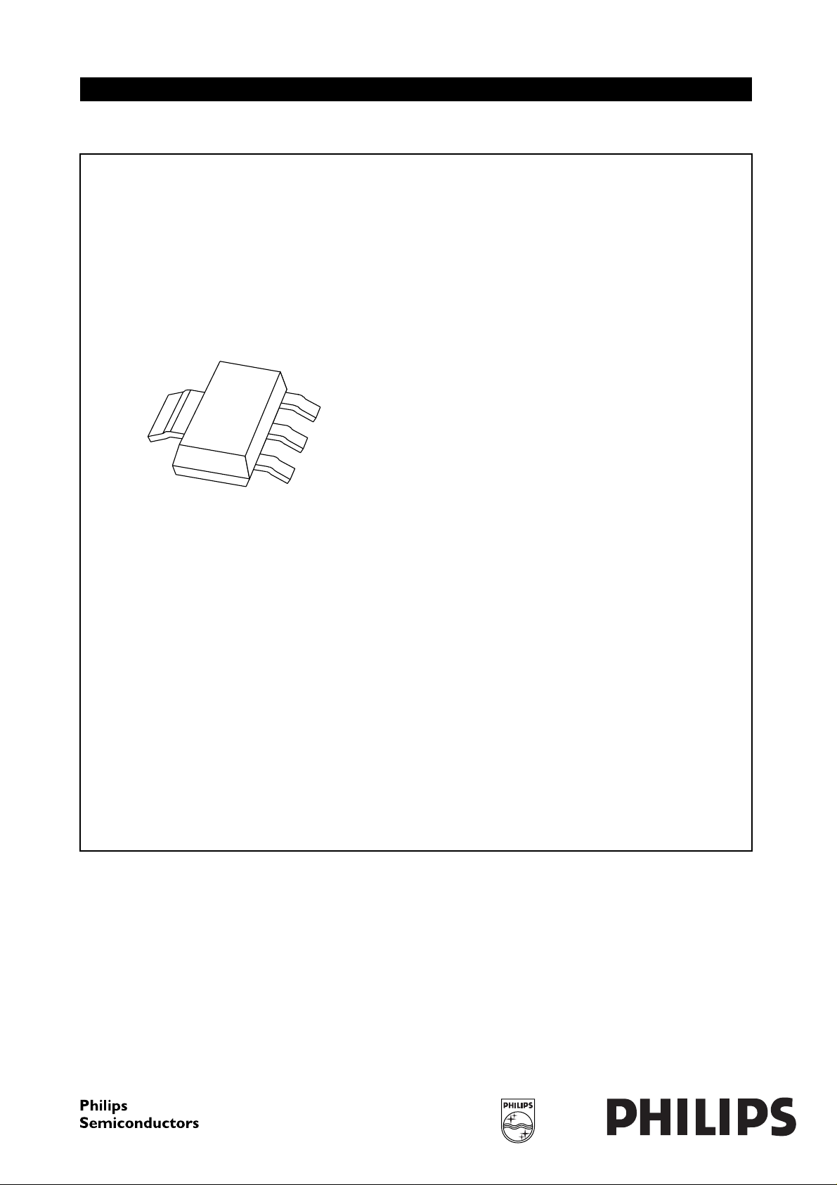
NPN transistor in a SOT223 plastic package.
PNP complement: PZTA56.
123
Top view
4
2, 4
1
3
MAM287
Fig.1 Simplified outline (SOT223) and symbol.
QUICK REFERENCE DATA
SYMBOL PARAMETER CONDITIONS MIN. MAX. UNIT
V
V
I
P
h
f
CBO
CEO
C
tot
FE
T
collector-base voltage open emitter − 80 V
collector-emitter voltage open base − 80 V
collector current (DC) − 500 mA
total power dissipation T
≤ 25 °C − 1.2 W
amb
DC current gain IC= 100 mA; VCE= 1 V 100 −
transition frequency IC= 10 mA; VCE= 2 V; f = 100 MHz 100 − MHz
1997 Jul 14 2

Philips Semiconductors Product specification
NPN general purpose transistor PZTA06
LIMITING VALUES
In accordance with the Absolute Maximum Rating System (IEC 134).
SYMBOL PARAMETER CONDITIONS MIN. MAX. UNIT
V
CBO
V
CEO
V
EBO
I
C
I
CM
I
BM
P
tot
T
stg
T
j
T
amb
Note
1. Device mounted on a printed-circuit board, single-sided copper, tinplated, mounting pad for collector 1 cm
mounting conditions, see
collector-base voltage open emitter − 80 V
collector-emitter voltage open base − 80 V
emitter-base voltage open collector − 4V
collector current (DC) − 500 mA
peak collector current − 800 mA
peak base current − 200 mA
total power dissipation T
≤ 25 °C; note 1 − 1.2 W
amb
storage temperature −65 +150 °C
junction temperature − 150 °C
operating ambient temperature −65 +150 °C
2
. For other
“Thermal considerations for SOT223 in the General part of handbook SC04”
.
THERMAL CHARACTERISTICS
SYMBOL PARAMETER CONDITIONS VALUE UNIT
R
R
th j-a
th j-s
thermal resistance from junction to ambient note 1 103 K/W
thermal resistance from junction to soldering point 22 K/W
Note
2
1. Device mounted on a printed-circuit board, single-sided copper, tinplated, mounting pad for collector 1 cm
mounting conditions, see
“Thermal considerations for SOT223 in the General part of handbook SC04”
. For other
.
CHARACTERISTICS
T
=25°C unless otherwise specified.
amb
SYMBOL PARAMETER CONDITIONS MIN. MAX. UNIT
I
CBO
I
EBO
h
V
V
f
T
FE
CEsat
BE
collector cut-off current IE= 0; VCB=80V − 50 nA
emitter cut-off current IC= 0; VEB=5V − 50 nA
DC current gain IC= 10 mA; VCE=1V 100 −
= 100 mA; VCE=1V 100 −
I
C
collector-emitter saturation voltage IC= 100 mA; IB=10mA − 250 mV
base-emitter voltage IC= 100 mA; VCE=1V − 1.2 V
transition frequency IC= 10 mA; VCE= 2 V; f = 100 MHz 100 − MHz
1997 Jul 14 3
 Loading...