

Philips PUMZ1 Datasheet
DISCRETE SEMICONDUCTORS
DATA SH EET
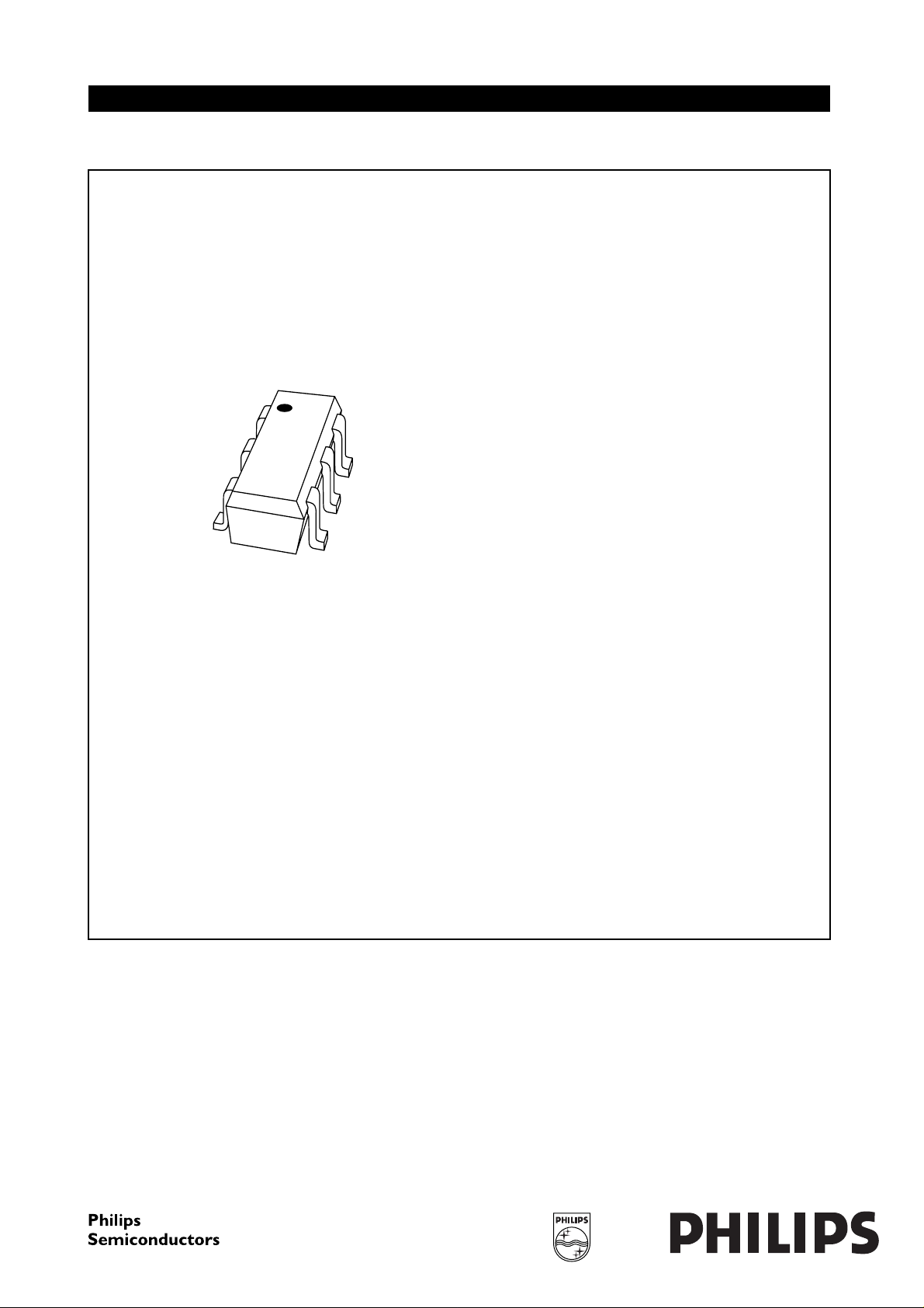
handbook, halfpage
MBD128
PUMZ1
NPN/PNP general purpose
transistors
Preliminary specification
Supersedes data of 1997 Jul 09
1999 Apr 14
Philips Semiconductors Preliminary specification
NPN/PNP general purpose transistors PUMZ1
FEATURES
• Low current (max. 100 mA)
• Low voltage (max. 40 V)
• Reduces number of components and boardspace.
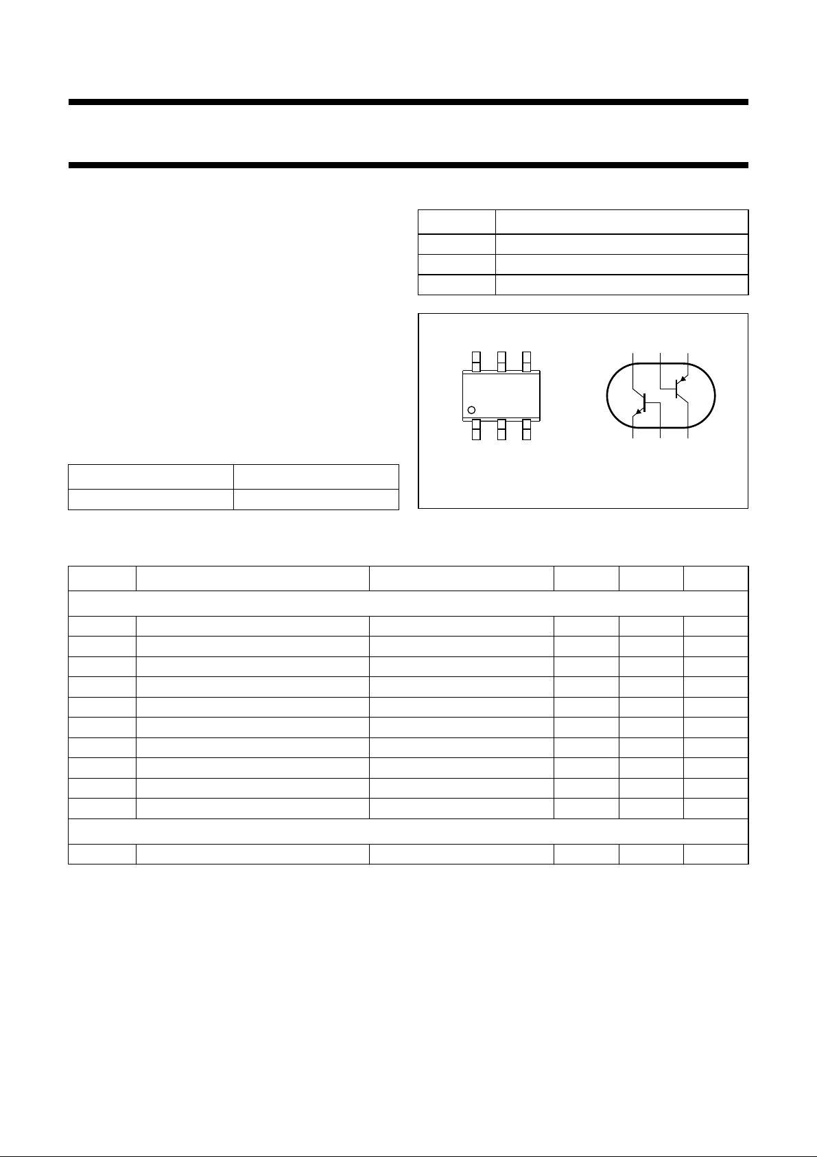
PINNING
PIN DESCRIPTION
1, 4 emitter TR2; TR1
2, 5 base TR2; TR1
3, 6 collector TR2; TR1
APPLICATIONS
• General purpose switching and amplification.
645
TR2
TR1
132
DESCRIPTION
Two independently operating NPN/PNP transistors in an
SC-88 plastic package.
MARKING
TYPE NUMBER MARKING CODE
handbook, halfpage
132
Top view
56
4
MAM341
Fig.1 Simplified outline (SC-88) and symbol.
PUMZ1 FtZ
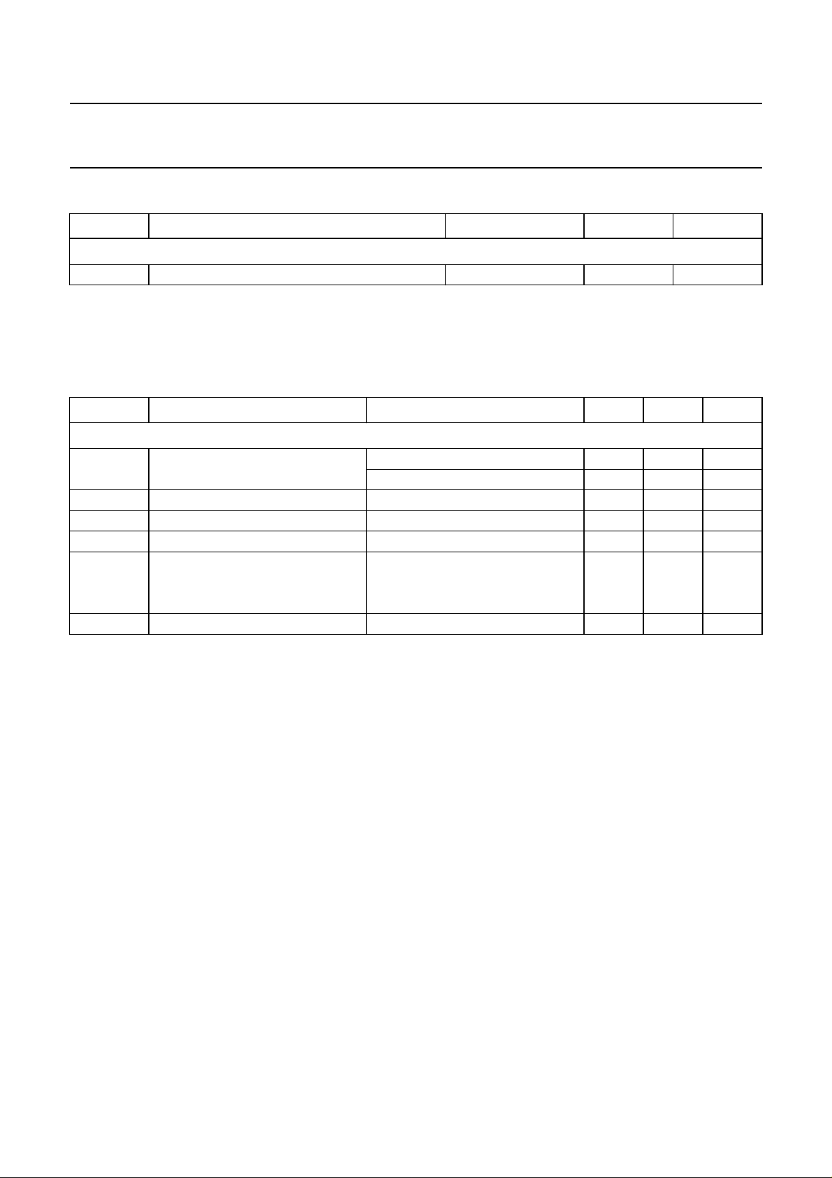
LIMITING VALUES
In accordance with the Absolute Maximum Rating System (IEC 134).
SYMBOL PARAMETER CONDITIONS MIN. MAX. UNIT
Per transistor; for the PNP transistor with negative polarity
V
CBO
V
CEO
V
EBO
I
C
I
CM
I
BM
P
tot
T
stg
T
j
T
amb
collector-base voltage open emitter − 50 V
collector-emitter voltage open base − 40 V
emitter-base voltage open collector − 5V
collector current (DC) − 100 mA
peak collector current − 200 mA
peak base current − 200 mA
total power dissipation T
≤ 25 °C − 200 mW
amb
storage temperature −65 +150 °C
junction temperature − 150 °C
operating ambient temperature −65 +150 °C
Per device
P
tot
total power dissipation T
≤ 25 °C; note 1 − 300 mW
amb
Note
1. Device mounted on an FR4 printed-circuit board.
1999 Apr 14 2
Philips Semiconductors Preliminary specification
NPN/PNP general purpose transistors PUMZ1
THERMAL CHARACTERISTICS
SYMBOL PARAMETER CONDITIONS VALUE UNIT
Per device
R
th j-a
Note
1. Device mounted on an FR4 printed-circuit board.
CHARACTERISTICS
=25°C unless otherwise specified.
T
amb
SYMBOL PARAMETER CONDITIONS MIN. MAX. UNIT
Per transistor; for the PNP transistor with negative polarity
I
CBO
I
EBO
h
FE
V
CEsat
C
c
f
T
thermal resistance from junction to ambient note 1 416 K/W
collector cut-off current IE= 0; VCB=30V − 100 nA
I
= 0; VCB=30V; Tj= 150 °C − 10 µA
E
emitter cut-off current IC= 0; VEB=4V − 100 nA
DC current gain IC= 1 mA; VCE= 6 V 120 −
collector-emitter saturation voltage IC= 50 mA; IB= 5 mA; note 1 − 200 mV
collector capacitance IE=ie= 0; VCB= 12 V; f = 1 MHz
TR1 − 1.5 pF
TR2 − 2.2 pF
transition frequency IC= 2 mA; VCE= 12 V; f = 100 MHz 100 − MHz
Note
1. Pulse test: t
≤ 300 µs; δ≤0.02.
p
1999 Apr 14 3
 Loading...