

Philips PUMT1 Datasheet
DISCRETE SEMICONDUCTORS
DATA SH EET
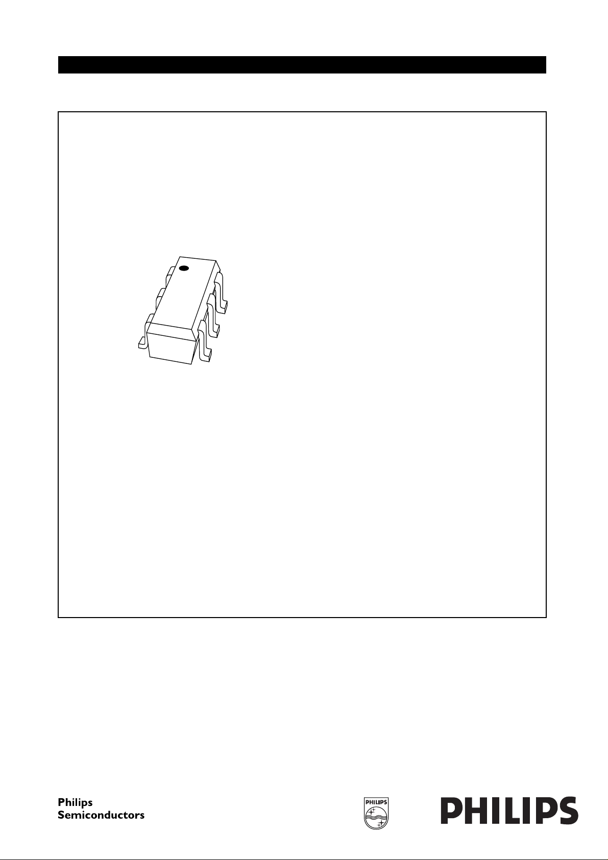
handbook, halfpage
MBD128
PUMT1
PNP general purpose
double transistor
Preliminary specification
Supersedes data of 1997 Jul 09
1999 Apr 14
Philips Semiconductors Preliminary specification
PNP general purpose double transistor PUMT1
FEATURES
• Low current (max. 100 mA)
• Low voltage (max. 40 V)
• Reduces number of components and boardspace.
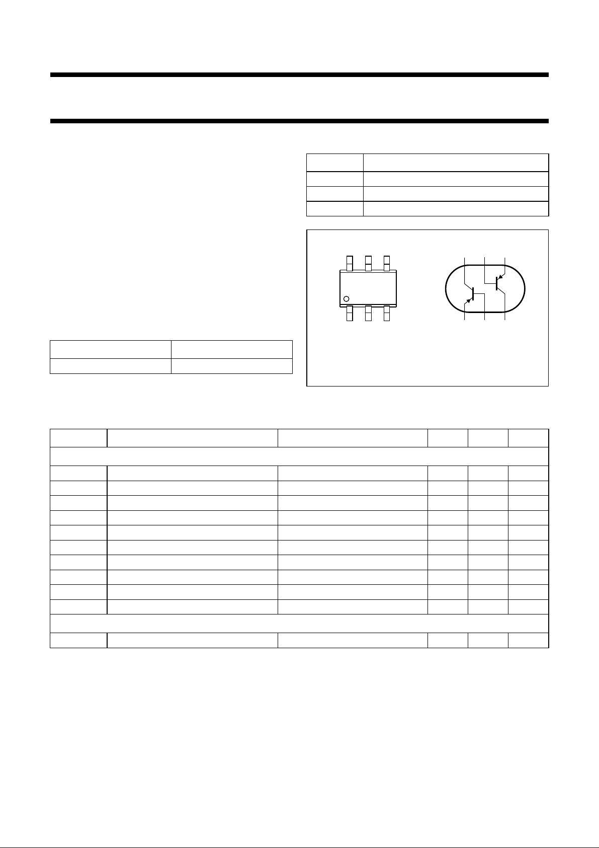
PINNING
PIN DESCRIPTION
1, 4 emitter TR1; TR2
2, 5 base TR1; TR2
3, 6 collector TR2; TR1
APPLICATIONS
• General purpose switching and amplification.
handbook, halfpage
DESCRIPTION
Two independently operating PNP transistors in an SC-88;
SOT363 plastic package. NPN complement: PUMX1.
MARKING
TYPE NUMBER MARKING CODE
Fig.1 Simplified outline (SC-88; SOT363)
PUMT1 FtF
LIMITING VALUES
In accordance with the Absolute Maximum Rating System (IEC 134).
132
Top view
and symbol.
56
4
MAM339
645
TR2
TR1
132
SYMBOL PARAMETER CONDITIONS MIN. MAX. UNIT
Per transistor
V
CBO
V
CEO
V
EBO
I
C
I
CM
I
BM
P
tot
T
stg
T
j
T
amb
collector-base voltage open emitter −−50 V
collector-emitter voltage open base −−40 V
emitter-base voltage open collector −−5V
collector current (DC) −−100 mA
peak collector current −−200 mA
peak base current −−200 mA
total power dissipation T
≤ 25 °C − 200 mW
amb
storage temperature −65 +150 °C
junction temperature − 150 °C
operating ambient temperature −65 +150 °C
Per device
P
tot
total power dissipation T
≤ 25 °C; note 1 − 300 mW
amb
Note
1. Device mounted on an FR4 printed-circuit board.
1999 Apr 14 2
Philips Semiconductors Preliminary specification
PNP general purpose double transistor PUMT1
THERMAL CHARACTERISTICS
SYMBOL PARAMETER CONDITIONS VALUE UNIT
Per device
R
th j-a
Note
1. Device mounted on an FR4 printed-circuit board.
CHARACTERISTICS
=25°C unless otherwise specified.
T
amb
SYMBOL PARAMETER CONDITIONS MIN. MAX. UNIT
Per transistor
I
CBO
I
EBO
h
FE
V
CEsat
C
c
f
T
thermal resistance from junction to ambient note 1 416 K/W
collector cut-off current IE= 0; VCB= −30 V −−100 nA
I
= 0; VCB= −30 V; Tj= 150 °C −−10 µA
E
emitter cut-off current IC= 0; VEB= −4V −−100 nA
DC current gain IC= −1 mA; VCE= −6 V 120 −
collector-emitter saturation
IC= −50 mA; IB= −5 mA; note 1 −−200 mV
voltage
collector capacitance IE=ie= 0; VCB= −12 V; f = 1 MHz − 2.2 pF
transition frequency IC= −2 mA; VCE= −12 V; f = 100 MHz 100 − MHz
Note
1. Pulse test: t
≤ 300 µs; δ≤0.02.
p
1999 Apr 14 3
 Loading...