

Page 1

查询PUMF12供应商
DISCRETE SEMICONDUCTORS
DATA SH EET
ook, halfpage
MBD128
PUMF12
PNP general purpose transistor;
NPN resistor-equipped transistor
Product specification 2002 Nov 07
Page 2
Philips Semiconductors Product specification
PNP general purpose transistor;
NPN resistor-equipped transistor
FEATURES
• General purpose transistor and resistor equipped
transistor in one package
• 100 mA collector current
• 50 V collector-emitter voltage
• 300 mW total power dissipation
• SOT363 package; replaces two SOT323 (SC-70)
packaged devices on same PCB area
• Reduced pick and place costs.
APPLICATIONS
• Power management switch for portable equipment,
e.g. cellular phone and CD player
• Switch for regulator.
DESCRIPTION
PNP general purpose transistor and an NPN
resistor-equipped transistor in a SOT363 (SC-88) plastic
package.
PUMF12
QUICK REFERENCE DATA
SYMBOL PARAMETER MAX. UNIT
TR1 (PNP)
V
CEO
I
C
I
CM
TR2 (NPN)
V
CEO
I
O
R1 bias resistor 22 kΩ
R2 bias resistor 47 kΩ
PINNING
PIN DESCRIPTION
1, 4 emitter TR1; TR2
2, 5 base TR1; TR2
6, 3 collector TR1; TR2
collector-emitter voltage −50 V
collector current (DC) −100 mA
peak collector current −200 mA
collector-emitter voltage 50 V
output current (DC) 100 mA
MARKING
TYPE NUMBER MARKING CODE
PUMF12 R2∗
Note
1. ∗ = p: Made in Hong Kong.
∗ = t: Made in Malaysia.
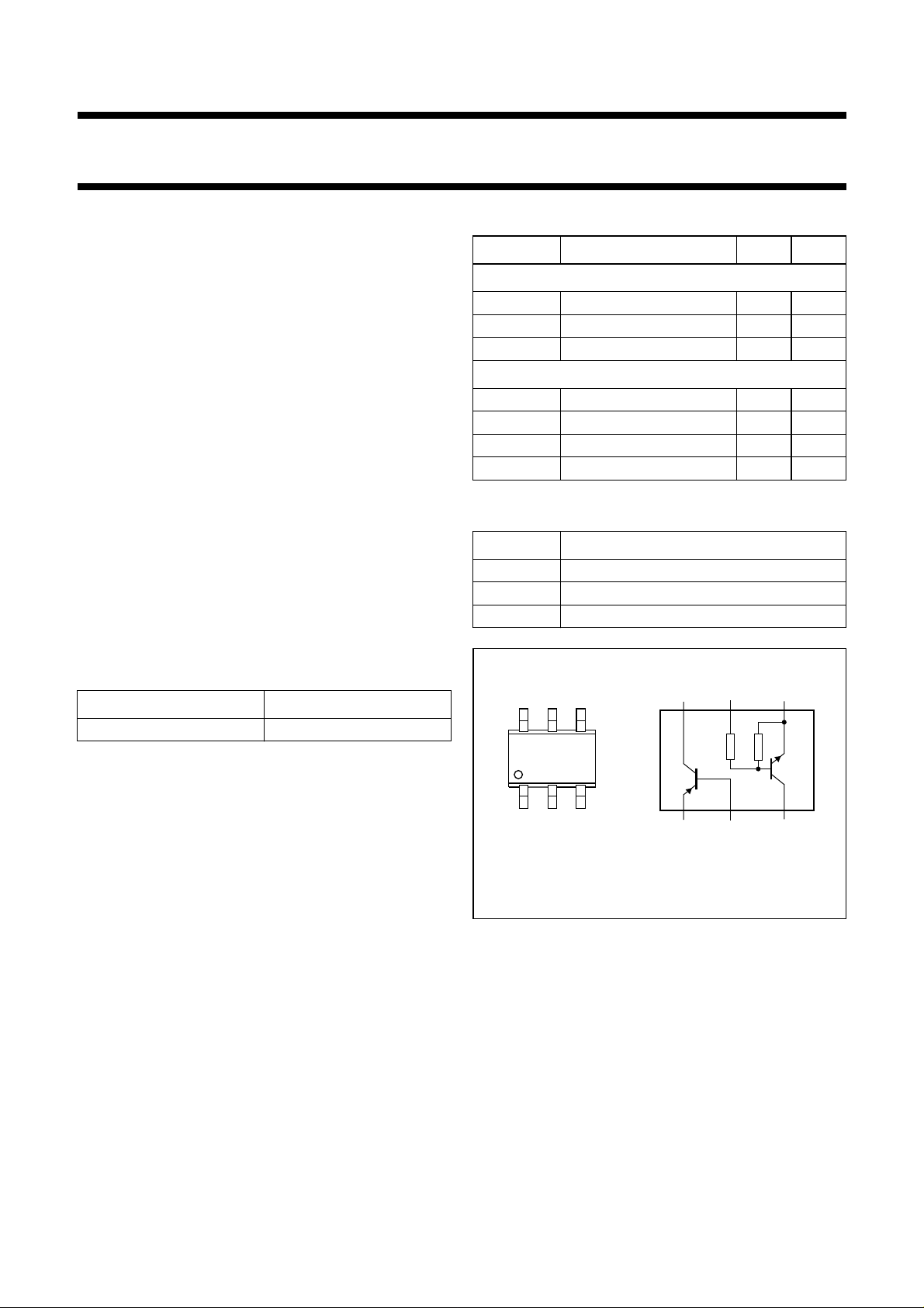
(1)
handbook, halfpage
132
Top view
56
4
MCE153
6
TR1
12 3
54
R1
Fig.1 Simplified outline (SOT363) and symbol.
R2
TR2
2002 Nov 07 2
Page 3
Philips Semiconductors Product specification
PNP general purpose transistor;
PUMF12
NPN resistor-equipped transistor
LIMITING VALUES
In accordance with the Absolute Maximum Rating System (IEC 60134).
SYMBOL PARAMETER CONDITIONS MIN. MAX. UNIT
Per transistor
P
tot
T
stg
T
j
T
amb
TR1 (PNP)
V
CBO
V
CEO
V
EBO
I
C
I
CM
TR2 (NPN)
V
CBO
V
CEO
V
EBO
V
i
I
O
I
CM
Per device
P
tot
total power dissipation T
≤ 25 °C; note 1 − 200 mW
amb
storage temperature range −65 +150 °C
junction temperature − 150 °C
operating ambient temperature −65 +150 °C
collector-base voltage open emitter −−50 V
collector-emitter voltage open base −−40 V
emitter-base voltage open collector −−5V
collector current (DC) −−100 mA
peak collector current −−200 mA
collector-base voltage open emitter − 50 V
collector-emitter voltage open base − 50 V
emitter-base voltage open collector − 10 V
input voltage
positive − +40 V
negative −−10 V
output current (DC) − 100 mA
peak collector current − 100 mA
total power dissipation T
≤ 25 °C; note 1 − 300 mW
amb
Note
1. Device mounted on an FR4 printed-circuit board.
THERMAL CHARACTERISTICS
SYMBOL PARAMETER CONDITIONS VALUE UNIT
R
th j-a
thermal resistance from junction to ambient note 1 416 K/W
Note
1. Device mounted on an FR4 printed-circuit board.
2002 Nov 07 3
Page 4

Philips Semiconductors Product specification
PNP general purpose transistor;
PUMF12
NPN resistor-equipped transistor
CHARACTERISTICS
T
=25°C unless otherwise specified.
amb
SYMBOL PARAMETER CONDITIONS MIN. TYP. MAX. UNIT
TR1 (PNP)
I
CBO
I
EBO
V
CEsat
h
FE
C
c
f
T
TR2 (NPN)
I
CBO
I
CEO
I
EBO
h
FE
V
CEsat
V
i(off)
V
i(on)
R1 input resistor 15.4 22 28.6 kΩ
R2
------R1
C
c
collector cut-off current VCB= −30 V; IE=0 −−−100 nA
V
= −30 V; IE= 0; Tj= 150 °C −−−10 µA
CB
emitter cut-off current VEB= −4 V; IC=0 −−−100 nA
saturation voltage IC= −50 mA; IB= −5 mA; note 1 −−−200 mV
DC current gain VCE= −6 V; IC= −1 mA 120 −−
collector capacitance VCB= −12 V; IE=ie= 0; f = 1 MHz −−2.2 pF
transition frequency VCE= −12 V; IC= −2 mA; f = 100 MHz 100 −−MHz
collector-base cut-off current VCB=50V; IE=0 −−100 nA
collector-emitter cut-off current VCE=30V; IB=0 −−1µA
V
=30V; IB= 0; Tj= 150 °C −−50 µA
CE
emitter-base cut-off current VEB=5V; IC=0 −−120 µA
DC current gain VCE=5V; IC= 5 mA 80 −−
saturation voltage IC= 10 mA; IB= 0.5 mA −−150 mV
input off voltage VCE=5V; IC= 100 µA − 0.9 0.5 V
input on voltage VCE= 0.3 V; IC= 2 mA 2 1.1 − V
resistor ratio 1.7 2.1 2.6
collector capacitance VCB=10V; IE=ie= 0; f = 1 MHz −−2.5 pF
Note
1. Device mounted on an FR4 printed-circuit board.
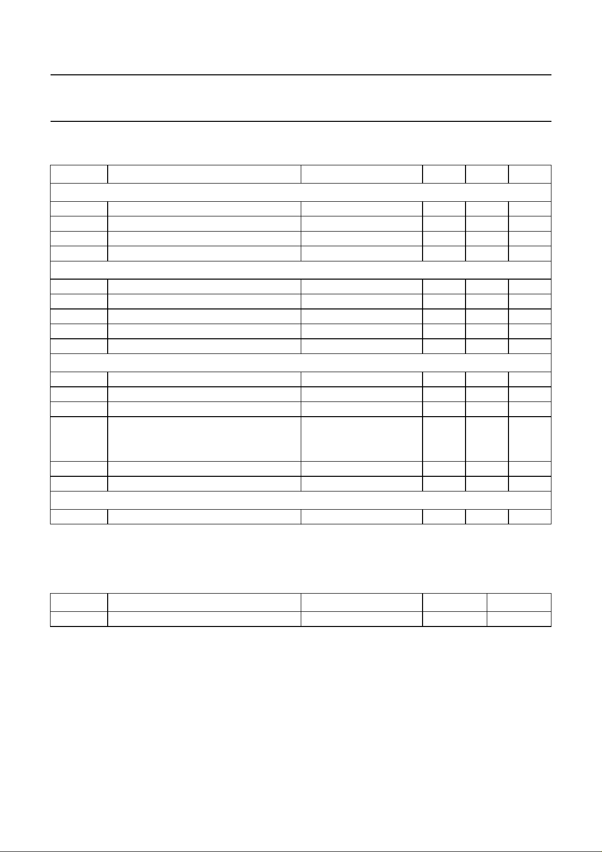
APPLICATION INFORMATION
R1
1
R
BE(ext)
R2
2
R
3
4
6
B(ext)
MHC322
handbook, halfpage
5
Fig.2 Typical power management circuit.
2002 Nov 07 4
Page 5

Philips Semiconductors Product specification
PNP general purpose transistor;
PUMF12
NPN resistor-equipped transistor
PACKAGE OUTLINE
Plastic surface mounted package; 6 leads SOT363
D
y
56
4
E
H
E
AB
X
v M
A
pin 1
index
132
e
1
DIMENSIONS (mm are the original dimensions)
A
UNIT
mm
A
1.1
0.8
max
0.1
1
b
p
0.30
0.25
0.20
0.10
b
p
e
cD
2.2
1.8
A
wBM
0 1 2 mm
scale
E
1.35
1.15
e
1.3
e
1
0.65
H
E
2.2
2.0
0.45
0.15
A
1
detail X
L
Qywv
p
0.25
0.15
Q
c
L
p
0.2 0.10.2
OUTLINE
VERSION
SOT363 SC-88
IEC JEDEC EIAJ
REFERENCES
2002 Nov 07 5
EUROPEAN
PROJECTION
ISSUE DATE
97-02-28
Page 6

Philips Semiconductors Product specification
PNP general purpose transistor;
PUMF12
NPN resistor-equipped transistor
DATA SHEET STATUS
LEVEL
I Objective data Development This data sheet contains data from the objective specification for product
II Preliminary data Qualification This data sheet contains data from the preliminary specification.
III Product data Production This data sheet contains data from the product specification. Philips
Notes
1. Please consult the most recently issued data sheet before initiating or completing a design.
2. The product status of the device(s) described in this data sheet may have changed since this data sheet was
3. For datasheets describing multiple type numbers, the highest-level product status determines the data sheet status.
DATA SHEET
STATUS
published. The latest information is available on the Internet at URL http://www.semiconductors.philips.com.
(1)
PRODUCT
STATUS
(2)(3)
development. Philips Semiconductors reserves the right to change the
specification in any manner without notice.
Supplementary data will be published at a later date. Philips
Semiconductors reserves the right to change the specification without
notice, in order to improve the design and supply the best possible
product.
Semiconductors reserves the right to make changes at any time in order
to improve the design, manufacturing and supply. Relevant changes will
be communicated via a Customer Product/Process Change Notification
(CPCN).
DEFINITION
DEFINITIONS
Short-form specification The data in a short-form
specification is extracted from a full data sheet with the
same type number and title. For detailed information see
the relevant data sheet or data handbook.
Limiting values definition Limiting values given are in
accordance with the Absolute Maximum Rating System
(IEC 60134). Stress above one or more of the limiting
values may cause permanent damage to the device.
These are stress ratings only and operation of the device
atthese or atanyother conditions above thosegivenin the
Characteristics sections of the specification is not implied.
Exposure to limiting values for extended periods may
affect device reliability.
Application information Applications that are
described herein for any of these products are for
illustrative purposes only. Philips Semiconductors make
norepresentationor warranty that suchapplicationswillbe
suitable for the specified use without further testing or
modification.
DISCLAIMERS
Life support applications These products are not
designed for use in life support appliances, devices, or
systems where malfunction of these products can
reasonably be expectedto result in personal injury.Philips
Semiconductorscustomersusing or selling theseproducts
for use in such applications do so at their own risk and
agree to fully indemnify Philips Semiconductors for any
damages resulting from such application.
Right to make changes Philips Semiconductors
reserves the right to make changes in the products including circuits, standard cells, and/or software described or contained herein in order to improve design
and/or performance. When the productis infull production
(status ‘Production’), relevant changes will be
communicated via a Customer Product/Process Change
Notification (CPCN). Philips Semiconductors assumes no
responsibility or liability for the use of any of these
products, conveys no licence or title under any patent,
copyright, or mask work right to these products, and
makes no representations or warranties that these
products are free from patent, copyright, or mask work
right infringement, unless otherwise specified.
2002 Nov 07 6
Page 7

Philips Semiconductors Product specification
PNP general purpose transistor;
NPN resistor-equipped transistor
PUMF12
NOTES
2002 Nov 07 7
Page 8

Philips Semiconductors – a w orldwide compan y
Contact information
For additional information please visit http://www.semiconductors.philips.com. Fax: +31 40 27 24825
For sales offices addresses send e-mail to: sales.addresses@www.semiconductors.philips.com.
© Koninklijke Philips Electronics N.V. 2002
All rights are reserved. Reproduction in whole or in part is prohibited without the prior written consent of the copyright owner.
The information presented in this document does not form part of any quotation or contract, is believed to be accurate and reliable and may be changed
without notice. No liability will be accepted by the publisher for any consequence of its use. Publication thereof does not convey nor imply any license
under patent- or other industrial or intellectual property rights.
Printed in The Netherlands 613514/01/pp8 Date of release: 2002 Nov 07 Document order number: 9397 750 10311
SCA74
 Loading...