

Philips PUMF11 User Guide

查询PUMF11供应商
DISCRETE SEMICONDUCTORS
DATA SH EET
ook, halfpage
MBD128
PUMF11
NPN resistor-equipped transistor;
PNP general purpose transistor
Product specification 2002 Apr 09
Philips Semiconductors Product specification
NPN resistor-equipped transistor;
PNP general purpose transistor
FEATURES
• Resistor-equipped transistor and general purpose
transistor in one package
• 100 mA collector current
• 50 V collector-emitter voltage
• 300 mW total power dissipation
• SOT363 package; replaces two SOT323 (SC-70)
packaged devices on same PCB area
• Reduced pick and place costs.
APPLICATIONS
• Power management switch for portable equipment,
e.g. cellular phone and CD player
• Switch for regulator.
DESCRIPTION
NPN resistor-equipped transistor and a PNP general
purpose transistor in a SOT363 (SC-88) plastic package.
PUMF11
QUICK REFERENCE DATA
SYMBOL PARAMETER MAX. UNIT
TR1 (NPN)
V
CEO
I
O
R1 bias resistor 22 kΩ
R2 bias resistor 47 kΩ
TR2 (PNP)
V
CEO
I
C
I
CM
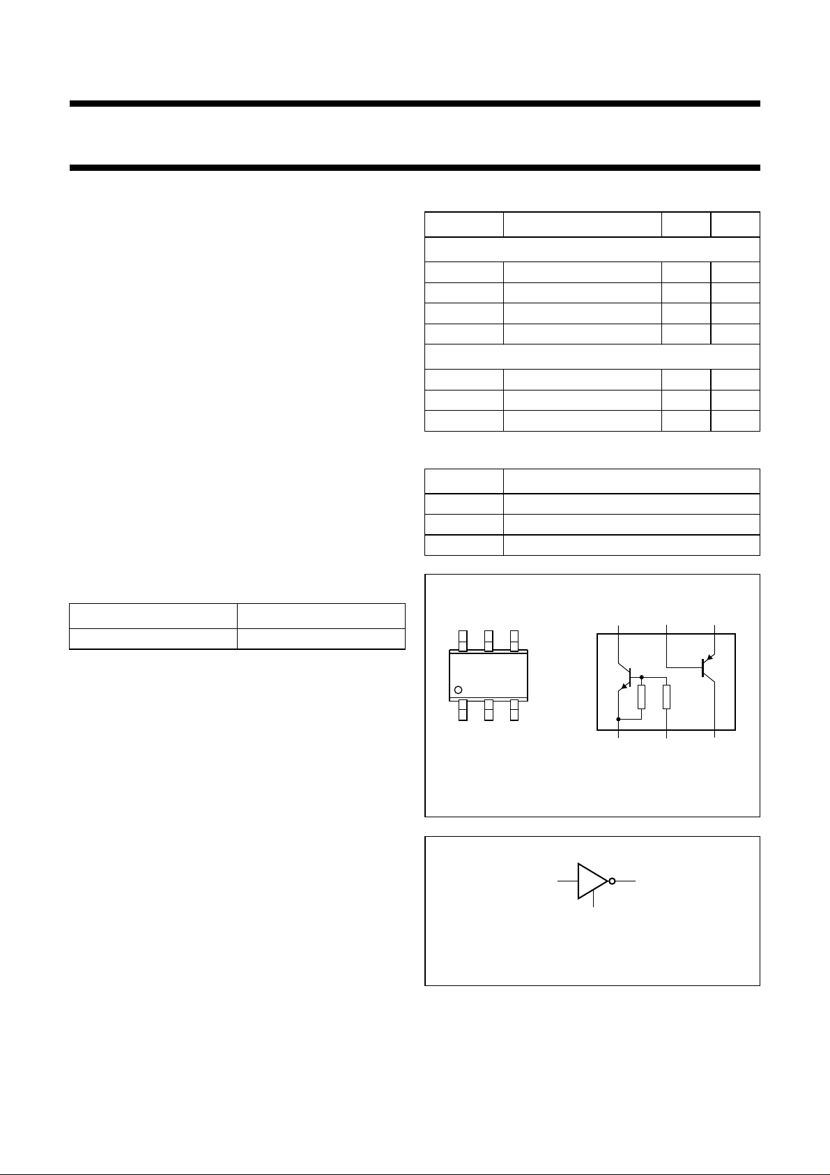
PINNING
PIN DESCRIPTION
1, 4 emitter TR1; TR2
2, 5 base TR1; TR2
6, 3 collector TR1; TR2
collector-emitter voltage 50 V
output current (DC) 100 mA
collector-emitter voltage 50 V
collector current (DC) 100 mA
peak collector current 200 mA
MARKING
TYPE NUMBER MARKING CODE
PUMF11 R1∗
Note
1. ∗ = p: Made in Hong Kong.
∗ = t: Made in Malaysia.
(1)
654
4
56
TR1
R2
R1
132
Top view
MAM465
123
Fig.1 Simplified outline (SOT363) and symbol.
2, 5
1, 4
MBK120
6, 3
Fig.2 Equivalent inverter symbol.
TR2
2002 Apr 09 2
Philips Semiconductors Product specification
NPN resistor-equippedtransistor;
PUMF11
PNP general purpose transistor
LIMITING VALUES
In accordance with the Absolute Maximum Rating System (IEC 60134).
SYMBOL PARAMETER CONDITIONS MIN. MAX. UNIT
Per transistor
P
tot
T
stg
T
j
T
amb
TR1 (NPN)
V
CBO
V
CEO
V
EBO
V
i
I
O
I
CM
TR2 (PNP)
V
CBO
V
CEO
V
EBO
I
C
I
CM
Per device
P
tot
total power dissipation T
≤ 25 °C; note 1 − 200 mW
amb
storage temperature −65 +150 °C
junction temperature − 150 °C
operating ambient temperature −65 +150 °C
collector-base voltage open emitter − 50 V
collector-emitter voltage open base − 50 V
emitter-base voltage open collector − 10 V
input voltage
positive − +40 V
negative −−10 V
output current (DC) − 100 mA
peak collector current − 100 mA
collector-base voltage open emitter −−50 V
collector-emitter voltage open base −−40 V
emitter-base voltage open collector −−5V
collector current (DC) −−100 mA
peak collector current −−200 mA
total power dissipation T
≤ 25 °C; note 1 − 300 mW
amb
Note
1. Device mounted on an FR4 printed-circuit board.
THERMAL CHARACTERISTICS
SYMBOL PARAMETER CONDITIONS VALUE UNIT
R
th j-a
thermal resistance from junction to ambient in free air; note 1 416 K/W
Note
1. Device mounted on an FR4 printed-circuit board.
2002 Apr 09 3
 Loading...