

Philips PUMD2 Datasheet

DISCRETE SEMICONDUCTORS
DATA SH EET
ook, halfpage
MBD128
PUMD2
NPN/PNP resistor-equipped
transistors
Product specification
Supersedes data of 1998 Aug 10
1999 May 21
Philips Semiconductors Product specification
NPN/PNP resistor-equipped transistors PUMD2
FEATURES
• Transistors with different polarity and built-in bias
resistors R1 and R2 (typ. 22 kΩ each)
• No mutual interference between the transistors
• Simplification of circuit design
• Reduces number of components and board space.
APPLICATIONS
• Especially suitable for space reduction in interface and
driver circuits
• Inverter circuit configurations without use of external
resistors.
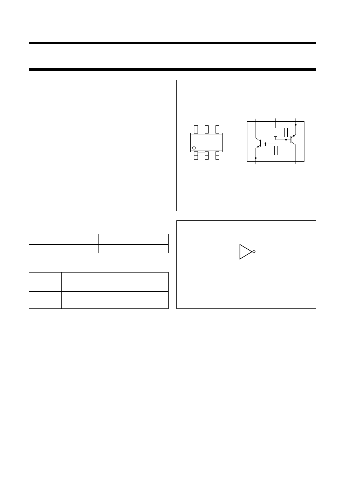
DESCRIPTION
NPN/PNP resistor-equipped transistors in an SC-88
plastic package.
handbook, halfpage
4
56
132
Top view
MAM343
Fig.1 Simplified outline (SC-88) and symbol.
654
R1 R2
TR1
R2
123
TR2
R1
MARKING
TYPE NUMBER MARKING CODE
PUMD2 Dt2
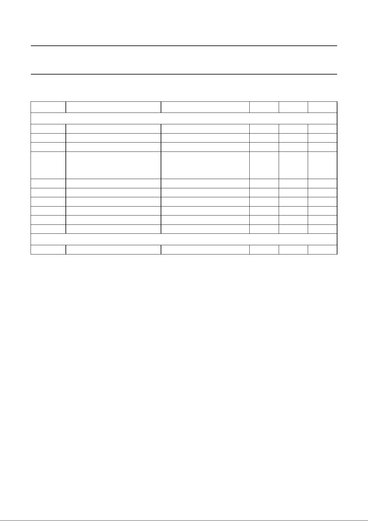
PINNING
PIN DESCRIPTION
1, 4 emitter TR1; TR2
2, 5 base TR1; TR2
6, 3 collector TR1; TR2
2, 5
1, 4
MBK120
6, 3
Fig.2 Equivalent inverter symbol.
1999 May 21 2
Philips Semiconductors Product specification
NPN/PNP resistor-equipped transistors PUMD2
LIMITING VALUES
In accordance with the Absolute Maximum Rating System (IEC 134).
SYMBOL PARAMETER CONDITIONS MIN. MAX. UNIT
Per transistor; for the PNP transistor with negative polarity
V
CBO
V
CEO
V
EBO
V
I
I
O
I
CM
P
tot
T
stg
T
j
T
amb
Per device
P
tot
collector-base voltage open emitter − 50 V
collector-emitter voltage open base − 50 V
emitter-base voltage open collector − 10 V
input voltage
positive − +40 V
negative −−10 V
output current (DC) − 100 mA
peak collector current − 100 mA
total power dissipation T
≤ 25 °C; note 1 − 200 mW
amb
storage temperature −65 +150 °C
junction temperature − 150 °C
operating ambient temperature −65 +150 °C
total power dissipation T
≤ 25 °C; note 1 − 300 mW
amb
Note
1. Device mounted on an FR4 printed-circuit board.
1999 May 21 3
Philips Semiconductors Product specification
NPN/PNP resistor-equipped transistors PUMD2
THERMAL CHARACTERISTICS
SYMBOL PARAMETER CONDITIONS VALUE UNIT
R
th j-a
Note
1. Device mounted on an FR4 printed-circuit board.
CHARACTERISTICS
=25°C unless otherwise specified.
T
amb
SYMBOL PARAMETER CONDITIONS MIN. TYP. MAX. UNIT
Per transistor; for the PNP transistor with negative polarity
I
CBO
I
CEO
I
EBO
h
FE
V
CEsat
V
i(off)
V
i(on)
R1 input resistor 15.4 22 28.6 kΩ
R2
------
R1
C
c
thermal resistance from junction to ambient note 1 416 K/W
collector cut-off current IE= 0; VCB=50V −−100 nA
collector cut-off current IB= 0; VCE=30V −−1µA
I
= 0; VCE=30V; Tj= 150 °C −−50 µA
B
emitter cut-off current IC= 0; VEB=5V −−180 µA
DC current gain IC= 5 mA; VCE=5V 60 −−
collector-emitter saturation
IC= 10 mA; IB= 0.5 mA −−150 mV
voltage
input-off voltage IC= 100 µA; VCE=5V − 1.1 0.8 V
input-on voltage IC= 5 mA; VCE= 300 mV 2.5 1.7 − V
resistor ratio 0.8 1 1.2
collector capacitance IE=ie= 0; VCB= 10 V; f = 1 MHz
TR1 (NPN) −−2.5 pF
TR2 (PNP) −−3pF
1999 May 21 4
 Loading...