

Page 1

INTEGRATED CIRCUITS
PTN3501
Maintenance and control device
Product specification
Supersedes data of 2000 Nov 22
2001 Jan 17
Page 2
Philips Semiconductors Product specification
Type number
PTN3501Maintenance and control device
FEA TURES
2
•I
C to parallel port expander
•Internal 256x8 E
2
PROM
•Self timed write cycle (5 ms typ.)
•16 byte page write operation
•Controlled pull-up on address lines
•Low voltage V
range of +2.5 V to +3.6 V
CC
•5 V – tolerant I/Os
•Low standby current (< 60 µA )
•Power on Reset
•Supports Live Insertion
•Compatible with SMBus specification version 1.1
•High E
2
PROM endurance and data retention
•Available in TSSOP20 package
DESCRIPTION
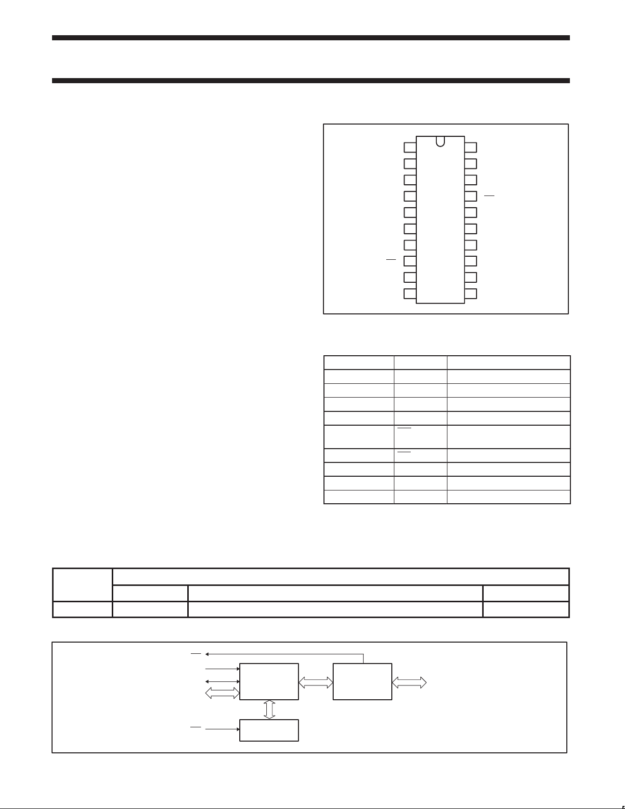
The PTN3501 is a general purpose maintenance and control device.
It features an on-board E
codes or board manufacturing data for read–back by application
software for diagnostic purposes.
The eight quasi bidirectional data pins can be independently
assigned as inputs or outputs to monitor board level status or
activate indicator devices such as LEDs.
The PTN3501 has six address pins allowing up to 64 devices to
share the common two wire I2C software protocol serial data bus.
The PTN3501 supports live insertion to facilitate usage in removable
cards on backplane systems.
The PTN3501 is an alternative to the functionally similar PTN3500
for systems where a high number of devices are required to share
the same I
2
C-bus without need for an additional I2C-bus I/O
expander.
2
PROM that can be used to store error
PIN CONFIGURATION
1
A0
2
A1
A2
3
4
P0
PTN3501
5
P1
P2
6
P3
7
8
INT
A5 A3
9
V
10
SS
Figure 1.
20
V
DD
19
SDA
18
SCL
17
WC
16
P7
15
P6
14
P5
13
P4
12
11
A4
SW00657
PIN DESCRIPTION
PIN NUMBER SYMBOL NAME AND FUNCTION
1,2,3,9,11,12 A0:5 Address Lines
4,5,6,7 P0:3 Quasi–bidirectional I/O pins
10 V
SS
13,14,15,16 P4:7 Quasi–bidirectional I/O pins
17 WC Write Control Pin. Should be
8 INT Interrupt Pin
18 SCL I2C Serial Clock
19 SDA I2C Serial Data
20 V
DD
Ground
tied LOW.
Supply Voltage
ORDERING INFORMATION
Package
Name Description Version
PTN3501DH TSSOP20 Plastic thin shrink small-outline package; 20 leads; body width 4.4 mm SOT360-1
FUNCTIONAL DIAGRAM
INT
SCL
SDA
A5:0
WC
2001 Jan 17 853-2227 25436
I2C
CONTROL
E2PROM
256 × 8
Figure 2.
2
8-BIT
I/O PORT
P7:0
SW00647
Page 3

Philips Semiconductors Product specification
PTN3501Maintenance and control device
CHARACTERISTICS OF THE I2C-BUS
The I2C-bus is for 2-way, 2-line communication between different ICs
or modules. The two lines are a serial data line (SDA) and a serial
clock line (SCL). Both lines must be connected to a positive supply
via a pull-up resistor when connected to the output stages of a device.
Data transfer may be initiated only when the bus is not busy.
Bit transfer
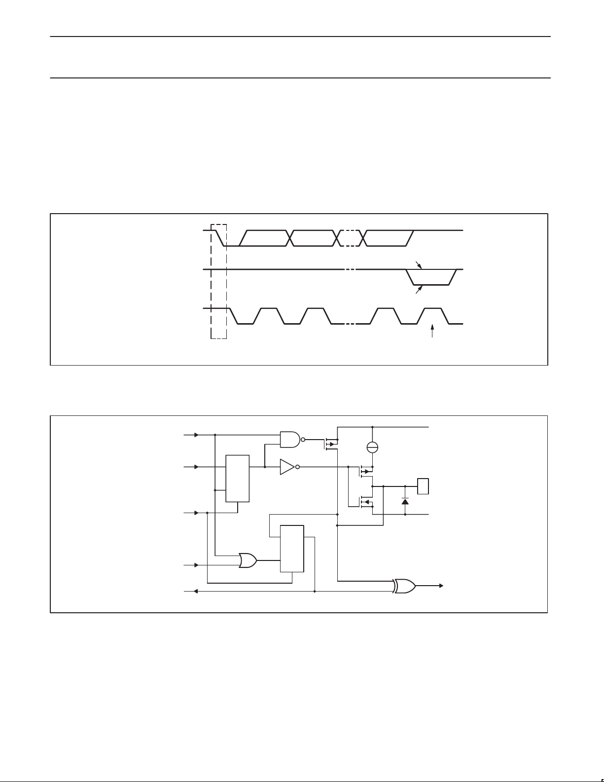
One data bit is transferred during each clock phase. The data on the
SDA line must remain stable during the HIGH period of the clock
pulse as changes in the data line at this time will be interpreted as
control signals (See Figure 3).
SDA
SCL
Start and stop conditions
Both data and clock lines remain HIGH when the bus is not busy. A
HIGH-to-LOW transition of the data line, while the clock is HIGH is
defined as the start condition (S). A LOW-to-HIGH transition of the
data line while the clock is HIGH is defined as the stop condition (P)
(see Figure 4).
System configuration
A device generating a message is a “transmitter”, a device receiving
is the “receiver”. The device that controls the message is the
“master” and the devices which are controlled by the master are the
“slaves” (see Figure 5).
SDA
SCL
SDA
SCL
START CONDITION STOP CONDITION
MASTER
TRANSMITTER/
RECEIVER
DATA LINE
STABLE;
DATA VALID
CHANGE
OF DATA
ALLOWED
Figure 3. Bit transfer
S
Figure 4. Definition of start and stop conditions
SLAVE
RECEIVER
SLAVE
TRANSMITTER/
RECEIVER
MASTER
TRANSMITTER
P
SW00542
SDA
SW00543
MASTER
TRANSMITTER/
RECEIVER
SCL
2001 Jan 17
SW00544
Figure 5. System configuration
3
Page 4
Philips Semiconductors Product specification
PTN3501Maintenance and control device
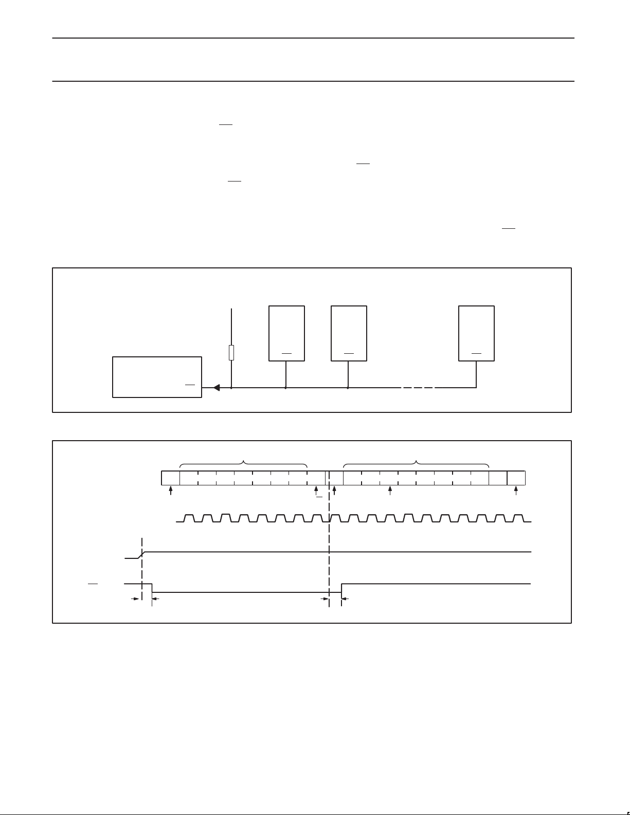
Acknowledge (see Figure 6)
The number of data bytes transferred between the start and the stop
conditions from transmitter to receiver is not limited. Each byte of
eight bits is followed by one acknowledge bit. The acknowledge bit
is a HIGH level put on the bus by the transmitter whereas the
master generates an extra acknowledge related clock pulse.
A slave receiver which is addressed must generate an acknowledge
after the reception of each byte. Also a master must generate an
acknowledge after the reception of each byte that has been clocked
DATA OUTPUT
BY TRANSMITTER
DATA OUTPUT
BY RECEIVER
SCL FROM
MASTER
S
START
CONDITION
Figure 6. Acknowledgment on the I2C-bus
out of the slave transmitter. The device that acknowledges has to
pull down the SDA line during the acknowledge clock pulse, so that
the SDA line is stable LOW during the HIGH period of the
acknowledge related clock pulse, set–up and hold times must be
taken into account.
A master receiver must signal an end of data to the transmitter by
not generating an acknowledge on the last byte that has been
clocked out of the slave. In this event the transmitter must leave the
data line HIGH to enable the master to generate a stop condition.
NOT ACKNOWLEDGE
ACKNOWLEDGE
9821
CLOCK PULSE FOR
ACKNOWLEDGEMENT
SW00545
FUNCTIONAL DESCRIPTION
WRITE PULSE
DATA FROM
SHIFT REGISTER
POWER-ON
RESET
READ PULSE
DATA TO
SHIFT REGISTER
100 µA
DQ
FF
C
I
S
DQ
FF
C
I
S
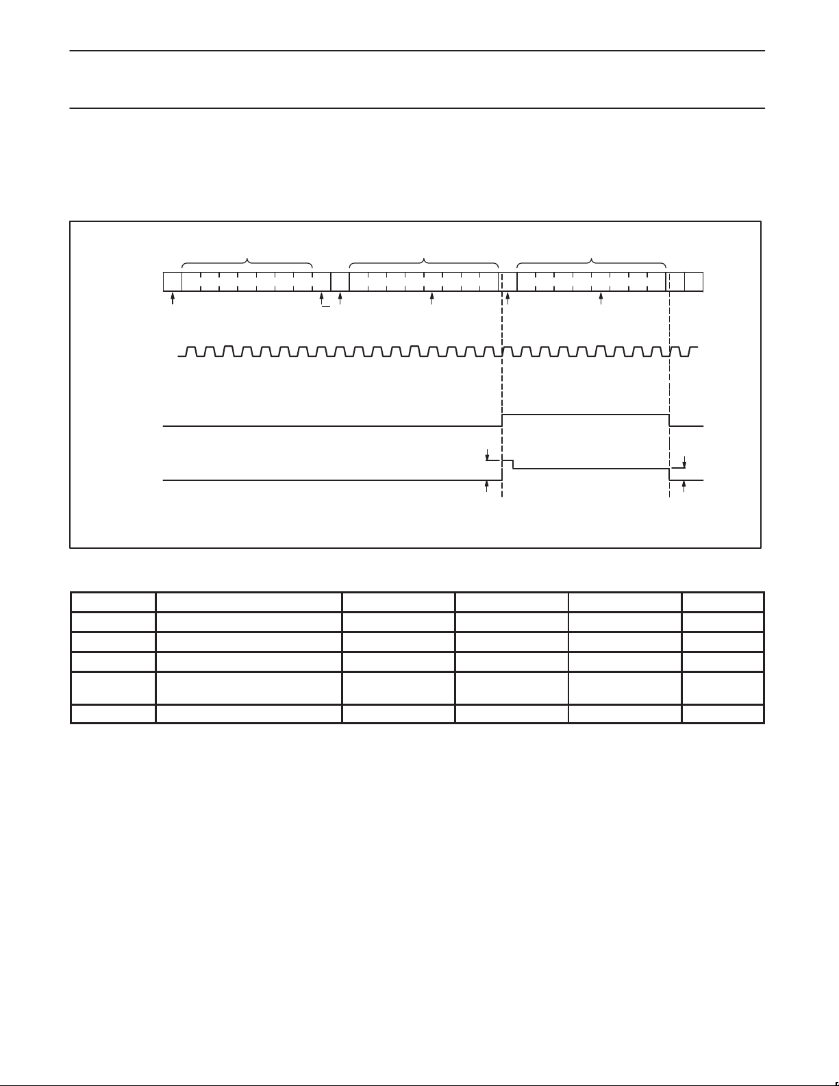
Figure 7. Simplified schematic diagram of each I/O
V
DD
P0 TO P7
V
SS
TO INTERRUPT LOGIC
SW00788
2001 Jan 17
4
Page 5

Philips Semiconductors Product specification
PTN3501Maintenance and control device
Addressing
For addressing, see Figure 8.
SLAVE ADDRESSSLAVE ADDRESS
S 0 A5 A4 A3 A2 A1 A0 0 A A5 0 AS 1 A4 A3 A2 A1 A0
(a) I/O EXPANDER
(b) MEMORY
a. b.
SW00648
Figure 8. PTN3501 slave addresses
Asynchronous Start
Following any Start condition on the bus, a minimum of 9 SCL clock cycles must be completed before a Stop condition can be issued. The
device does not support a Stop or a repeated Start condition during this time period.
I/O OPERATIONS (see also Figure 7)
Each of the PTN3501’s eight I/Os can be independently used as an input or output. Input I/O data is transferred from the port to the
microcontroller by the READ mode (See Figure 10). Output data is transmitted to the port by the I/O WRITE mode (see Figure 9).
WRITE TO
PORT
DATA OUT
FROM PORT
SCL
12345678
SLAVE ADDRESS (I/O EXPANDER)
S 0 A5 A4 A3 A2 A1 A0 0 A DATA 1 A DATA 2 ASDA
DATA TO PORT
ACKNOWLEDGE
R/WSTART CONDITION ACKNOWLEDGE
FROM SLAVE
t
pv
FROM SLAVE
DATA TO PORT
t
pv
ACKNOWLEDGE
FROM SLAVE
DATA 2 VALIDDATA 1 VALID
READ FROM
PORT
DATA INTO
PORT
2001 Jan 17
Figure 9. I/O WRITE mode (output)
SLAVE ADDRESS (I/O EXPANDER) DATA FROM PORT DATA FROM PORT
S 0 A5 A4 A3 A2 A1 A0 1 A DATA 1 A
START CONDITION ACKNOWLEDGE
DATA 1
INT
t
iv
R/W ACKNOWLEDGE
t
ph
Figure 10. I/O READ mode (input)
FROM SLAVE
DATA 2 DATA 3
5
FROM MASTER
t
ps
SW00649
1SDA
DATA 4
DATA 4
t
ir
P
STOP
CONDITION
SW00650
Page 6
Philips Semiconductors Product specification
PTN3501Maintenance and control device
Interrupt (see Figs 11 and 12)
The PTN3501 provides an open drain output (INT) which can be fed
to a corresponding input of the microcontroller. This gives these
chips a type of master function which can initiate an action
elsewhere in the system.
An interrupt is generated by any rising or falling edge of the port
inputs in the input mode. After time t
the signal INT is valid.
iv
Resetting and reactivating the interrupt circuit is achieved when data
on the port is changed to the original setting or data is read from or
written to the port which has generated the interrupt.
Resetting occurs as follows:
•In the READ mode at the acknowledge bit after the rising edge of
the SCL signal
PTN3501
(1)
INT
MICROCONTROLLER
INT
V
DD
•In the WRITE mode at the acknowledge bit after the
HIGH–to–LOW transition of the SCL signal
•Returning of the port data to its original setting. A second port
state change will require an SCL rising clock edge to be captured
as an INT
event.
•Interrupts which occur during the acknowledge clock pulse may
be lost (or very short) due to the resetting of the interrupt during
this pulse.
Each change of the I/Os after resetting will be detected and, after
the next rising clock edge, will be transmitted as INT. Reading from
or writing to another device does not affect the interrupt circuit.
PTN3501
(2)
INT
PTN3501
(16)
INT
SW00790
DATA
INTO P5
INT
SCL
Figure 11. Application of multiple PTN3501s with interrupt
SLAVE ADDRESS (I/O EXPANDER)
S 0 A5 A4 A3 A2 A1 A0 1 A 1 1SDA
ACKNOWLEDGE
R/WSTART CONDITION STOP CONDITION
FROM SLAVE
12345678
t
iv
t
ir
DATA FROM PORT
P
P5
SW00791
Figure 12. Interrupt generated by a change of input to I/O P5
2001 Jan 17
6
Page 7
Philips Semiconductors Product specification
PTN3501Maintenance and control device
Quasi-bidirectional I/Os (see Figure 13)
A quasi-bidirectional I/O can be used as an input or output without the use of a control signal for data direction. At power-on the I/Os are HIGH.
In this mode, only a current source to V
These devices turn on when an output is written HIGH, and are switched off by the negative edge of SCL. The I/Os should be HIGH before
being used as inputs.
is active. An additional strong pull-up to VDD allows fast rising edges into heavily loaded outputs.
DD
P3
OUTPUT
VOLTAGE
P3
PULL-UP
OUTPUT
CURRENT
SYMBOL
t
pv
t
ps
t
ph
t
iv
t
ir
SLAVE ADDRESS (PTN3501)
S 0 A2 A1 A0 0 A A ASDA
SCL
A5A4A
12345678
3
Figure 13. Transient pull-up current I
DATA TO PORT
1
ACKNOWLEDGE
R/WSTART CONDITION ACKNOWLEDGE
FROM SLAVE
while P3 changes from LOW-to-HIGH and back to LOW
OHt
P3
I
OHt
FROM SLAVE
DATA TO PORT
0
P3
PARAMETER MIN TYP MAX UNIT
Output data valid; CL ≤ 100 pF – – 4 µs
Input data setup time; CL ≤ 100 pF 0 – – µs
Input data hold time; CL ≤ 100 pF 4 – – µs
Interrupt input data valid time;
C
≤ 100 pF
L
– – 4 µs
Interrupt reset time; CL ≤ 100 pF – – 4 µs
P
I
OH
SW00789
2001 Jan 17
7
Page 8
Philips Semiconductors Product specification
PTN3501Maintenance and control device
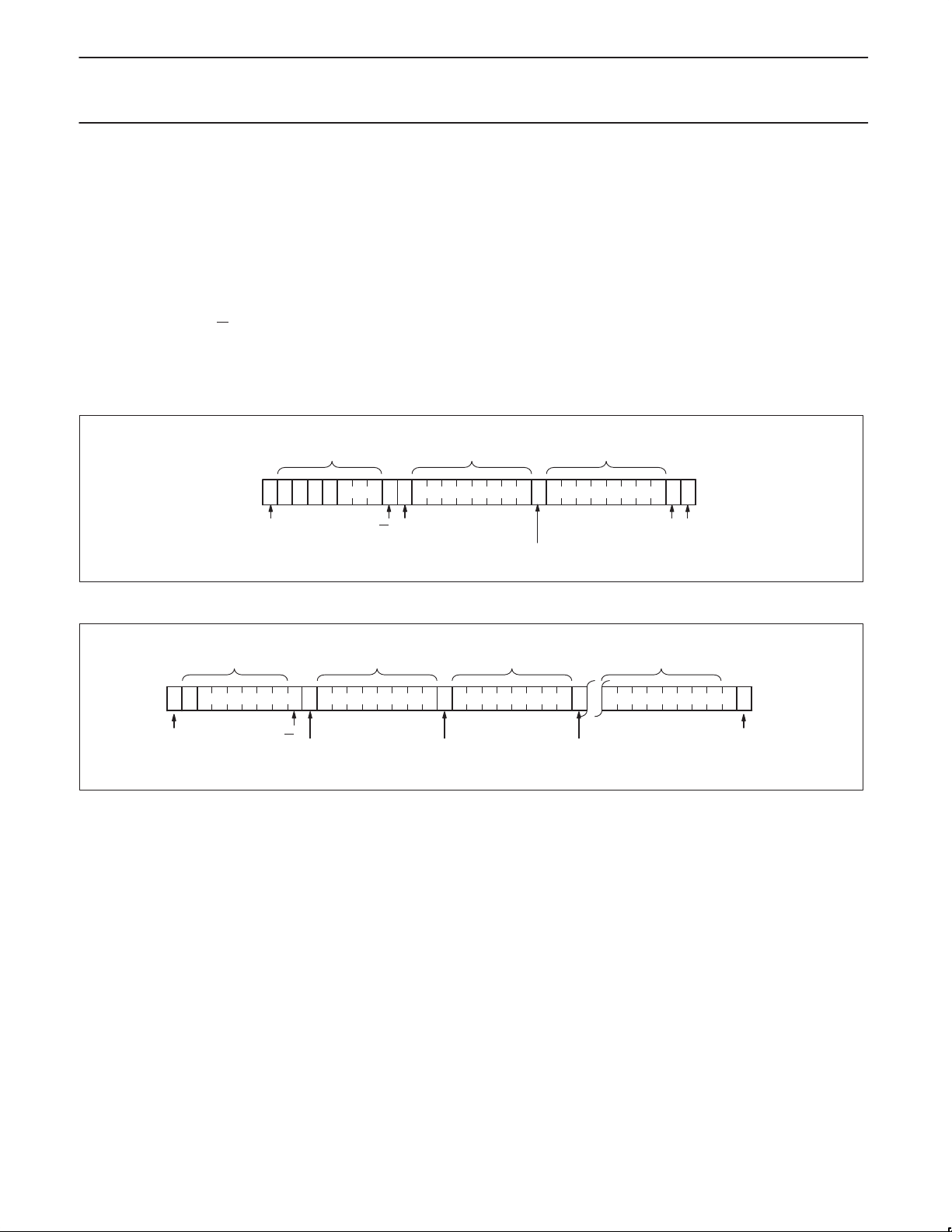
MEMORY OPERATIONS
Write operations
Write operations require an additional address field to indicate the
memory address location to be written. The address field is eight
bits long providing access to any one of the 256 words of memory.
There are two types of write operations, byte write and page write.
Byte Write (see Figure 14)
To perform a byte write the start condition is followed by the memory
slave address and the R/W
with an acknowledge and then consider the next eight bits sent as
the word address and the eight bits after the word address as the
data. The PTN3501 will issue an acknowledge after the receipt of
both the word address and the data. To terminate the data transfer
bit set to 0. The PTN3501 will respond
SLAVE
ADDRESS
(MEMORY)
SDA
S 1 A5 A4 A3 A2 A1 A0 A A
START CONDITION STOP
0A
ACKNOWLEDGE
R/W
FROM SLAVE
Figure 14. Byte write
the master issues the stop condition, initiating the internal write cycle
to the non–volatile memory. Only write and read operations to the
quasi–bidirectional I/Os are allowed during the internal write cycle.
Page Write (see Figure 15)
A page write is initiated in the same way as the byte write, if after
sending the first word of data, the stop condition is not received the
PTN3501 considers subsequent words as data. After each data
word the PTN3501 responds with an acknowledge and the four least
significant bits of the memory address field are incremented. Should
the master not send a stop condition after 16 data words the
address counter will return to its initial value and overwrite the data
previously written. After the receipt of the stop condition the inputs
will behave as with the byte write during the internal write cycle.
WORD
ADDRESS
ACKNOWLEDGE
FROM SLAVE
DATA
ACKNOWLEDGE
FROM SLAVE
P
CONDITION
SW00651
SDA
SLAVE ADDRESS
(MEMORY)
1 A5A4A3A2A1A0
S
START
CONDITION
WORD ADDRESS
AA
0
R/W
ACKNOWLEDGE
FROM SLAVE
DATA TO MEMORY
DATA n
ACKNOWLEDGE
FROM SLAVE
Figure 15. Page Write
DATA TO MEMORY
A
ACKNOWLEDGE
FROM SLAVE
DATA +3n
P
A
STOP
CONDITION
SW00652
2001 Jan 17
8
Page 9
Philips Semiconductors Product specification
PTN3501Maintenance and control device
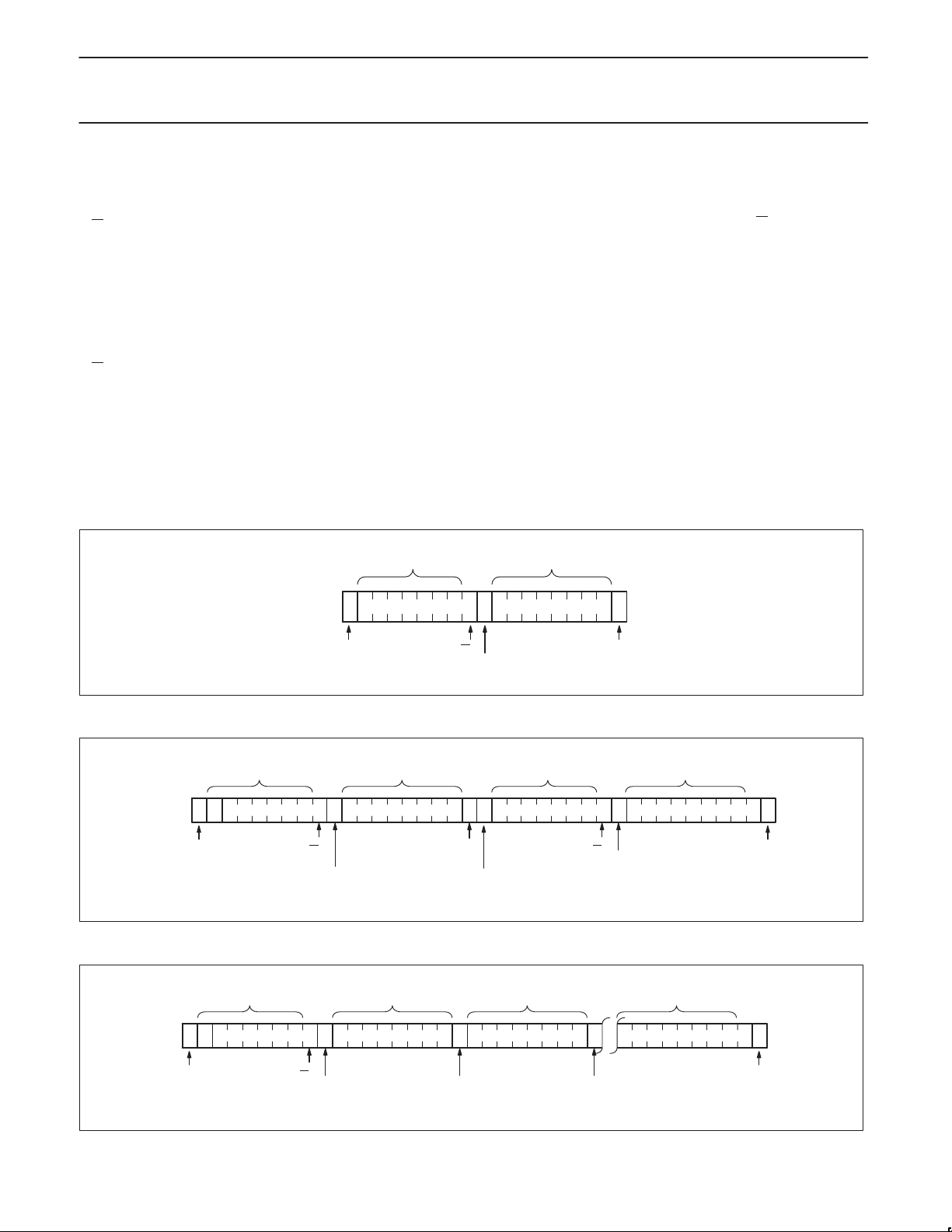
Read operations
PTN3501 read operations are initiated in an identical manner to
write operations with the exception that the memory slave address’
R/W
bit is set to a one. There are three types of read operations;
current address, random and sequential.
Current Address Read (see Figure 16)
The PTN3501 contains an internal address counter that increments
after each read or write access, as a result if the last word accessed
was at address n then the address counter contains the address
n+1.
When the PTN3501 receives its memory slave address with the
R/W
bit set to one it issues an acknowledge and uses the next eight
clocks to transmit the data contained at the address stored in the
address counter. The master ceases the transmission by issuing the
stop condition after the eighth bit. There is no ninth clock cycle for
the acknowledge.
Random Read (see Figure 17)
The PTN3501’s random read mode allows the address to be read
from to be specified by the master. This is done by performing a
dummy write to set the address counter to the location to be read.
SLAVE ADDRESS
(MEMORY)
SDA
1A5A4A3A2A1A0 1 A
S
The master must perform a byte write to the address location to be
read, but instead of transmitting the data after receiving the
acknowledge from the PTN3501 the master reissues the start
condition and memory slave address with the R/W
bit set to one.
The PTN3501 will then transmit an acknowledge and use the next
eight clock cycles to transmit the data contained in the addressed
location. The master ceases the transmission by issuing the stop
condition after the eighth bit, omitting the ninth clock cycle
acknowledge.
Sequential Read (see Figure 18)
The PTN3501 sequential read is an extension of either the current
address read or random read. If the master doesn’t issue a stop
condition after it has received the eighth data bit, but instead issues
an acknowledge, the PTN3501 will increment the address counter
and use the next eight cycles to transmit the data from that location.
The master can continue this process to read the contents of the
entire memory . Upon reaching address 255 the counter will return to
address 0 and continue transmitting data until a stop condition is
received. The master ceases the transmission by issuing the stop
condition after the eighth bit, omitting the ninth clock cycle
acknowledge.
DATA FROM MEMORY
P
SDA
SDA
SLAVE ADDRESS
(MEMORY)
1 A5A4A3A2A1A0
S
START
CONDITION
SLAVE ADDRESS
(MEMORY)
1 A5A4A3A2A1 A0
S
START
CONDITION
R/W
1
R/W
START
CONDITION
Figure 16. Current Address Read
ADDRESS
AA0
ACKNOWLEDGE
FROM SLAVE
DATA
FROM MEMORY
A
ACKNOWLEDGE
FROM SLAVE
DATA n
R/W
ACKNOWLEDGE
FROM SLAVE
WORD
ACKNOWLEDGE
FROM SLAVE
SLAVE ADDRESS
(MEMORY)
S
1A5 A4A3A2A1A0
START
CONDITION
Figure 17. Random Read
DATA
FROM MEMORY
DATA n+1
A
ACKNOWLEDGE
FROM MASTER
Figure 18. Sequential Read
STOP
CONDITION
SW00653
DATA FROM MEMORY
A
1
R/W
ACKNOWLEDGE
FROM SLAVE
A
ACKNOWLEDGE
FROM MASTER
DATA
FROM MEMORY
DATA N+X
SW00655
P
STOP
CONDITION
SW00654
P
STOP
CONDITION
2001 Jan 17
9
Page 10
Philips Semiconductors Product specification
PTN3501Maintenance and control device
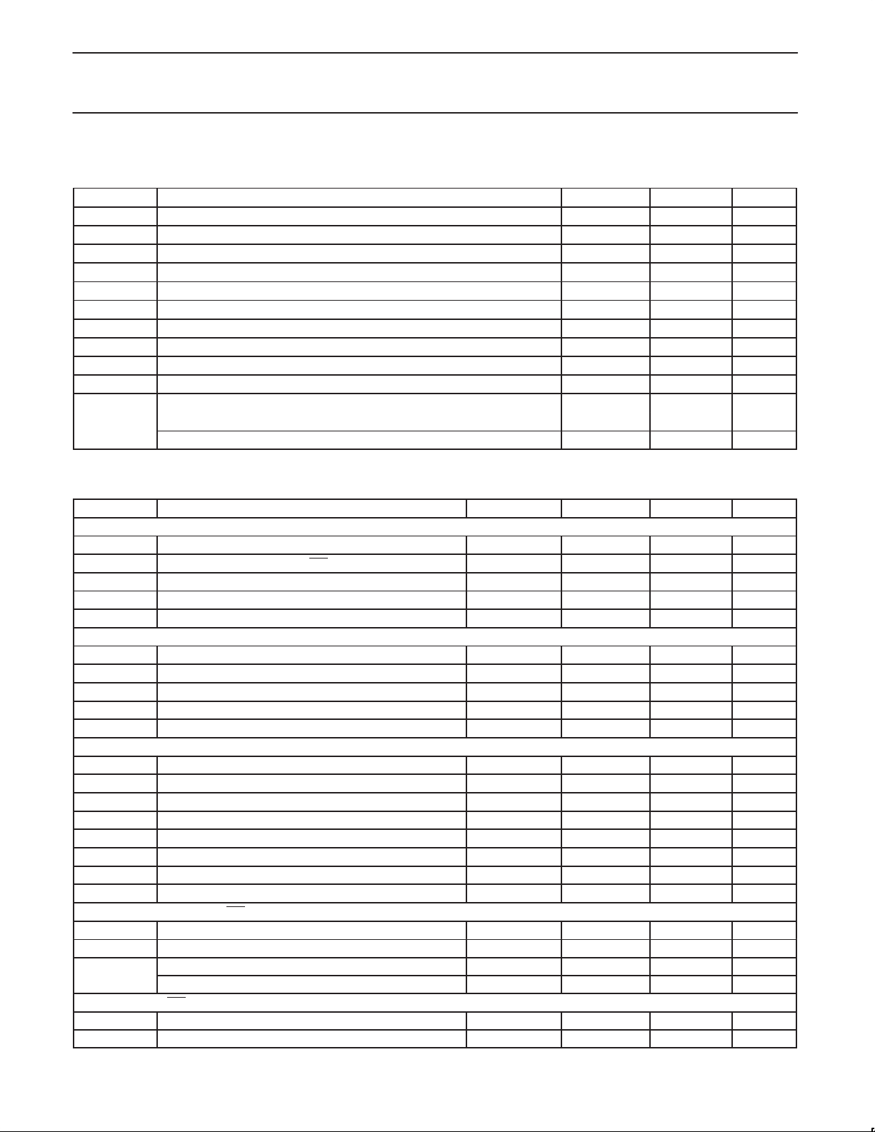
ABSOLUTE MAXIMUM RATINGS
Absolute Maximum Ratings are those values beyond which damage to the device may occur. Functional operation under these conditions is not implied.
SYMBOL
V
CC
V
I
I
I
I
O
I
DD
I
SS
P
tot
P
O
T
STG
T
AMB
V
ESD
Supply Voltage –0.5 4.0 V
Input Voltage V
DC Input Current –20 20 mA
DC Output Current –25 25 mA
Supply Current –100 100 mA
Supply Current –100 100 mA
Total Power Dissipation – 400 mW
Total Power Dissipation per Output – 100 mW
Storage Temperature –65 +150
Operating Temperature –40 +85
Electrostatic Discharge:
Human Body Model, 1.5 kΩ, 100 pF – >2000 V
Machine Model, 0 Ω, 200 pF – >200 V
PARAMETER MIN MAX UNIT
– 0.5 5.5 V
SS
_C
_C
DC ELECTRICAL CHARACTERISTICS
T
= –40_C to +85_C unless otherwise specified; VCC = 3.3 V
amb
SYMBOL PARAMETER MIN TYP MAX UNIT
Supply
V
DD
I
DDQ
I
DD1
I
DD2
V
POR
Input SCL; input, output SDA
V
IL
V
IH
I
OL
I
L
C
I
I/O Expander Port
V
IL
V
IH
I
IHL(max)
I
OL
I
OH
I
OHt
C
I
C
O
Address Inputs A0 thru A5, WC input
V
IL
V
IH
I
L
Interrupt output INT
I
OL
I
L
Supply Voltage 2.5 3.3 3.6 V
Standby Current; A0 thru A5, WC = HIGH – 60 µA
Supply Current Read – – 1 mA
Supply Current Write – – 2 mA
Power on Reset Voltage – – 2.4 V
Input LOW voltage –0.5 – 0.3 V
Input HIGH voltage 0.7 V
Output LOW current @ V
Input leakage current @ V
Input capacitance @ VI = V
= 0.4 V 3 – – mA
OL
= VDD or V
I
SS
SS
–1 – 1 µA
– – 7 pF
DD
– 5.5 V
Input LOW voltage –0.5 – 0.3 V
Input HIGH voltage 0.7 V
DD
– 5.5 V
DD
DD
Input current through protection diodes –400 – 400 µA
Output LOW current @ V
Output HIGH current @ V
= 1 V 10 25 – mA
OL
OH
= V
ss
30 100 300 µA
Transient pull–up current – 2 – mA
Input Capacitance – – 10 pF
Output Capacitance – – 10 pF
Input LOW voltage –0.5 – 0.3 V
Input HIGH voltage 0.7 V
Input leakage current @ V
Input leakage (pull-up) current @ V
I
= V
DD
I
= V
SS
–1 – 1 µA
10 25 100 µA
DD
– 5.5 V
DD
Low level output current; VOL = 0.4 V 1.6 – – mA
Leakage current @ VI = VDD or V
SS
–1 – +1 µA
V
V
V
2001 Jan 17
10
Page 11
Philips Semiconductors Product specification
PTN3501Maintenance and control device
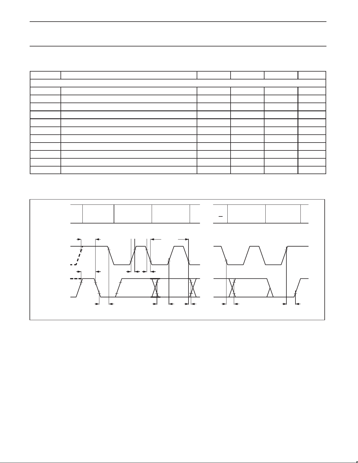
I2C-BUS TIMING CHARACTERISTICS
SYMBOL PARAMETER MIN. TYP. MAX. UNIT
I2C-bus timing (see Figure 19; Note 1)
f
SCL
t
SW
t
BUF
t
SU;STA
t
HD;STA
t
r
t
f
t
SU;DAT
t
HD;DAT
t
VD;DAT
t
SU;STO
NOTE:
1. All the timing values are valid within the operating supply voltage and ambient temperature range and refer to V
voltage swing of V
SCL clock frequency – – 400 kHz
tolerable spike width on bus – – 50 ns
bus free time 1.3 – – µs
STAR T condition set–up time 0.6 – – µs
STAR T condition hold time 0.6 – – µs
SCL and SDA rise time – – 0.3 µs
SCL and SDA fall time – – 0.3 µs
data set–up time 250 – – ns
data hold time 0 – – ns
SCL LOW to data out valid – – 1.0 µs
STOP condition set–up time 0.6 – – µs
and VIH with an input
SS
to VDD.
IL
handbook, full pagewidth
PROTOCOL
t
SCL
SDA
START
CONDITION
SU;STA
t
BUF
(S)
t
HD;STA
BIT 7
MSB
(A7)
t
r
t
f
t
SU;DAT
1 / f
BIT 6
(A6)
SCL
t
HD;DAT
BIT 0
LSB
(R/W)
ACKNOWLEDGE
t
VD;DAT
(A)
MBD820
STOP
CONDITION
(P)
t
SU;STO
SW00561
Figure 19.
2001 Jan 17
11
Page 12
Philips Semiconductors Product specification
PTN3501Maintenance and control device
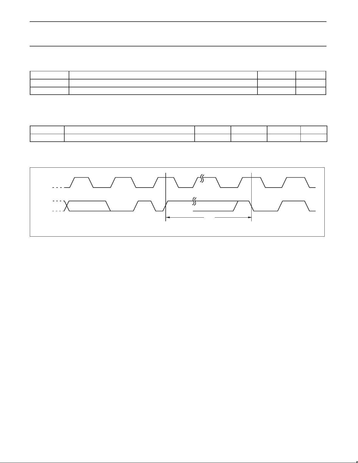
POWER-UP TIMING
SYMBOL PARAMETER MAX. UNIT
1
t
PUR
1
t
PUW
NOTE:
and t
1. t
PUR
guaranteed by design.
are the delays required from the time VCC is stable until the specified operation can be initiated. These parameters are
PUW
WRITE CYCLE LIMITS
SYMBOL PARAMETER MIN. TYP.
1
t
WR
Write Cycle Time – 5 10 ms
NOTE:
is the maximum time that the device requires to perform the internal write operation.
1. t
WR
Write Cycle Timing
SCL
Power-up to Read Operation 1 ms
Power-up to Write Operation 5 ms
(5)
MAX. UNIT
SDA
8th Bit
Word n
ACK
Stop
Condition
Figure 20.
MEMORY
t
WR
Start
Condition
ADDRESS
SW00560
2001 Jan 17
12
Page 13

Philips Semiconductors Product specification
PTN3501Maintenance and control device
SOLDERING
Introduction
There is no soldering method that is ideal for all IC packages. Wave
soldering is often preferred when through-hole and surface mounted
components are mixed on one printed-circuit board. However, wave
soldering is not always suitable for surface mounted ICs, or for
printed-circuits with high population densities. In these situations
reflow soldering is often used.
This text gives a very brief insight to a complex technology. A more
in-depth account of soldering ICs can be found in our
Databook
(order code 9398 652 90011).
IC Package
DIP
Soldering by dipping or by wave
The maximum permissible temperature of the solder is 260°C;
solder at this temperature must not be in contact with the joint for
more than 5 seconds. The total contact time of successive solder
waves must not exceed 5 seconds.
The device may be mounted up to the seating plane, but the
temperature of the plastic body must not exceed the specified
maximum storage temperature (T
has been pre-heated, forced cooling may be necessary immediately
after soldering to keep the temperature within the permissible limit.
Repairing soldered joints
Apply a low voltage soldering iron (less than 24 V) to the lead(s) of
the package, below the seating plane or not more than 2 mm above
it. If the temperature of the soldering iron bit is less than 300°C it
may remain in contact for up to 10 seconds. If the bit temperature is
between 300 and 400°C, contact may be up to 5 seconds.
max). If the printed-circuit board
stg
SO and SSOP
Reflow soldering
Reflow soldering techniques are suitable for all SO and SSOP
packages.
Reflow soldering requires solder paste (a suspension of fine solder
particles, flux and binding agent) to be applied to the printed-circuit
board by screen printing, stencilling or pressure-syringe dispensing
before package placement.
Several techniques exist for reflowing; for example, thermal
conduction by heated belt. Dwell times vary between 50 and 300
seconds depending on heating method. Typical reflow temperatures
range from 215 to 250°C.
Preheating is necessary to dry the paste and evaporate the binding
agent. Preheating duration: 45 minutes at 45°C.
Wave soldering
Wave soldering is not recommended for SSOP packages. This is
because of the likelihood of solder bridging due to closely-spaced
leads and the possibility of incomplete solder penetration in
multi-lead devices.
If wave soldering cannot be avoided, the following conditions
must be observed:
•A double-wave (a turbulent wave with high upward pressure
followed by a smooth laminar wave) soldering technique
should be used.
•The longitudinal axis of the package footprint must be
parallel to the solder flow and must incorporate solder
thieves at the downstream end.
Even with these conditions, only consider wave soldering
SSOP packages that have a body width of 4.4 mm, that is
SSOP16 (SOT369–1) or SSOP20 (SOT266–1).
During placement and before soldering, the package must be fixed
with a droplet of adhesive. The adhesive can be applied by screen
printing, pin transfer or syringe dispensing. The package can be
soldered after the adhesive is cured.
Maximum permissible solder temperature is 260°C, and maximum
duration of package immersion in solder is 10 seconds, if cooled to
less than 150°C within 6 seconds. Typical dwell time is 4 seconds at
250°C.
A mildly-activated flux will eliminate the need for removal of
corrosive residues in most applications.
Repairing soldered joints
Fix the component by first soldering two diagonally opposite end
leads. Use only a low voltage soldering iron (less than 24 V) applied
to the flat part of the lead. Contact time must be limited to
10 seconds at up to 300 °C. When using a dedicated tool, all other
leads can be soldered in one operation within 2 to 5 seconds
between 270 and 320°C.
PURCHASE OF PHILIPS I2C COMPONENTS
Purchase of Philips I2C components conveys a license under the Philips’ I2C patent
to use the components in the I2C system provided the system conforms to the
I2C specifications defined by Philips. This specification can be ordered using the
code 9398 393 40011.
2001 Jan 17
13
Page 14
Philips Semiconductors Product specification
PTN3501Maintenance and control device
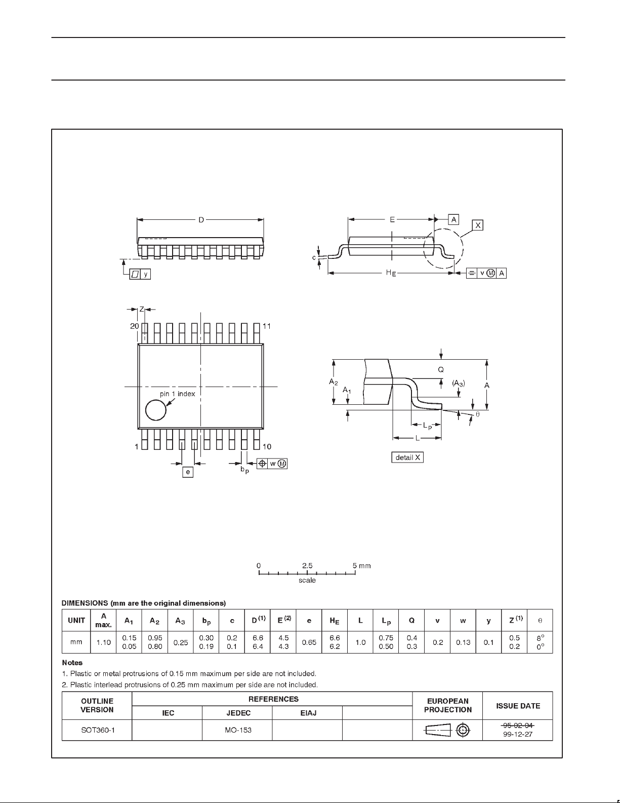
TSSOP20: plastic thin shrink small outline package; 20 leads; body width 4.4 mm SOT360-1
2001 Jan 17
14
Page 15

Philips Semiconductors Product specification
PTN3501Maintenance and control device
Data sheet status
Data sheet
status
Objective
specification
Preliminary
specification
Product
specification
Product
status
Development
Qualification
Production
Definition
This data sheet contains the design target or goal specifications for product development.
Specification may change in any manner without notice.
This data sheet contains preliminary data, and supplementary data will be published at a later date.
Philips Semiconductors reserves the right to make changes at any time without notice in order to
improve design and supply the best possible product.
This data sheet contains final specifications. Philips Semiconductors reserves the right to make
changes at any time without notice in order to improve design and supply the best possible product.
[1]
[1] Please consult the most recently issued datasheet before initiating or completing a design.
Definitions
Short-form specification — The data in a short-form specification is extracted from a full data sheet with the same type number and title. For
detailed information see the relevant data sheet or data handbook.
Limiting values definition — Limiting values given are in accordance with the Absolute Maximum Rating System (IEC 134). Stress above one
or more of the limiting values may cause permanent damage to the device. These are stress ratings only and operation of the device at these or
at any other conditions above those given in the Characteristics sections of the specification is not implied. Exposure to limiting values for extended
periods may affect device reliability.
Application information — Applications that are described herein for any of these products are for illustrative purposes only. Philips
Semiconductors make no representation or warranty that such applications will be suitable for the specified use without further testing or
modification.
Disclaimers
Life support — These products are not designed for use in life support appliances, devices or systems where malfunction of these products can
reasonably be expected to result in personal injury . Philips Semiconductors customers using or selling these products for use in such applications
do so at their own risk and agree to fully indemnify Philips Semiconductors for any damages resulting from such application.
Right to make changes — Philips Semiconductors reserves the right to make changes, without notice, in the products, including circuits, standard
cells, and/or software, described or contained herein in order to improve design and/or performance. Philips Semiconductors assumes no
responsibility or liability for the use of any of these products, conveys no license or title under any patent, copyright, or mask work right to these
products, and makes no representations or warranties that these products are free from patent, copyright, or mask work right infringement, unless
otherwise specified.
Philips Semiconductors
811 East Arques Avenue
P.O. Box 3409
Sunnyvale, California 94088–3409
Telephone 800-234-7381
Copyright Philips Electronics North America Corporation 2001
All rights reserved. Printed in U.S.A.
Date of release: 01-01
Document order number: 9397 750 07933
2001 Jan 17
15
 Loading...