

Philips Power Semiconductor Service Manual

S.M.P.S. Power Semiconductor Applications
Philips Semiconductors
CHAPTER 2
Switched Mode Power Supplies
2.1 Using Power Semiconductors in Switched Mode Topologies
(including transistor selection guides)
2.2 Output Rectification
2.3 Design Examples
2.4 Magnetics Design
2.5 Resonant Power Supplies
103


S.M.P.S. Power Semiconductor Applications
Philips Semiconductors
Using Power Semiconductors in Switched Mode Topologies
105


S.M.P.S. Power Semiconductor Applications
Philips Semiconductors
2.1.1 An Introduction to Switched Mode Power Supply
Topologies
Formanyyearstheworldof power supply designhas seen
a gradual movement away from the use of linear power
suppliestothemorepracticalswitchedmodepower supply
(S.M.P.S.). The linear power supply contains a mains
transformer and a dissipative seriesregulator. Thismeans
the supply has extremely large and heavy 50/60 Hz
transformers, and also very poor power conversion
efficiencies,both seriousdrawbacks. Typical efficienciesof
30% are standard for a linear. This compares with
efficiencies of between 70 and 80%, currently available
using S.M.P.S. designs.
Furthermore,by employing high switching frequencies, the
sizes of the power transformer and associated filtering
components in the S.M.P.S. are dramatically reduced in
comparison to the linear. For example, an S.M.P.S.
operating at 20kHz produces a 4 times reduction in
component size, and this increases to about 8 times at
100kHz and above. This means an S.M.P.S. design can
producevery compactand lightweightsupplies.This isnow
an essential requirement for the majority of electronic
systems.The supply must slot into an ever shrinking space
left for it by electronic system designers.
Outline
At the heart of theconverter is the highfrequency inverter
section, where the input supply is chopped at very high
frequencies(20to200kHzusingpresenttechnologies) then
filtered and smoothed to produce dc outputs. The circuit
configuration which determines how the power is
transferred is called the TOPOLOGY of the S.M.P.S.,and
is an extremely important part of the design process. The
topology consists of an arrangement of transformer,
inductors, capacitors and power semiconductors (bipolar
or MOSFET power transistors andpower rectifiers).
Presently, there is a very wide choice of topologies
available, each one having its own particular advantages
and disadvantages, making it suitable for specific power
supply applications. Basic operation, advantages,
drawbacks and most common areas of use for the most
commontopologies arediscussed inthe followingsections.
A selection guide to the Philips range of power
semiconductors (including bipolars, MOSFETs and
rectifiers) suitable for usein S.M.P.S. applications isgiven
at the end of each section.
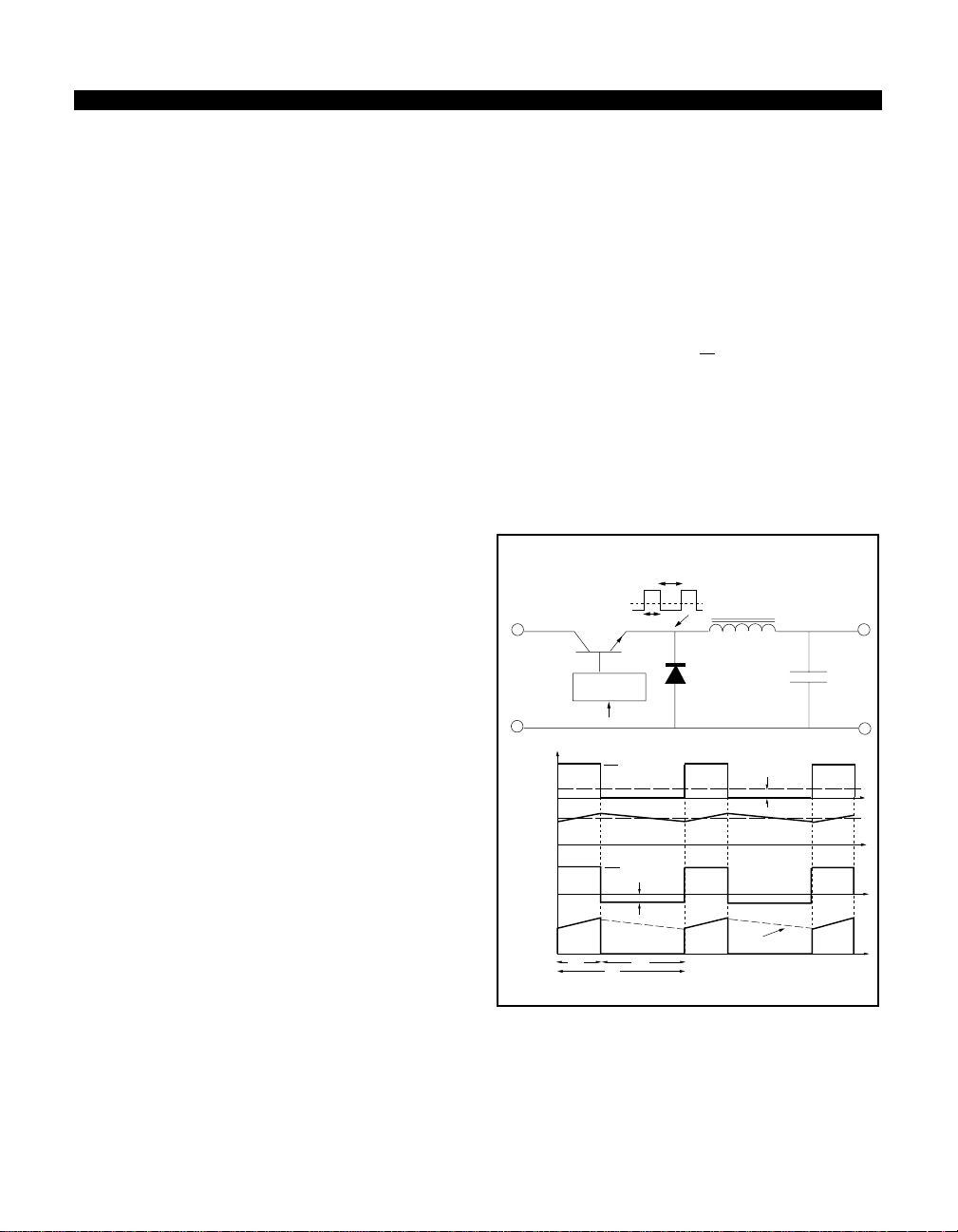
(1) Basic switched mode supply circuit.
An S.M.P.S. can be a fairly complicated circuit, as can be
seen from the block diagram shown in Fig. 1. (This
configuration assumes a 50/60Hz mains input supply is
used.) The ac supply is first rectified, and then filtered by
the input reservoir capacitor to produce a rough dc input
supply. This level can fluctuate widely due to variations in
the mains. In addition the capacitance on the input has to
be fairly large to hold up the supply in case of a severe
droop in the mains. (The S.M.P.S. can also be configured
tooperate fromany suitable dcinput, in thiscase thesupply
is called a dc to dc converter.)
ac input
supply
Input rectification
and filtering
duty cycle
High
Frequency
switch
mosfet or
control
bipolar
T
control
circuitry
Power
Transformer
PWM
OSC
Output rectification
and filtering
Vref
Fig. 1. Basic switched mode power supply block diagram.
107
dc output
voltage
S.M.P.S. Power Semiconductor Applications
Philips Semiconductors
Theunregulated dc isfed directly to the central block of the
supply, the high frequency power switching section. Fast
switchingpowersemiconductordevices suchas MOSFETs
and Bipolars are driven on and off, and switch the input
voltage across the primary of the power transformer. The
drive pulses are normally fixed frequency (20 to 200kHz)
and variable duty cycle. Hence, a voltage pulse train of
suitable magnitude and duty ratio appears on the
transformer secondaries. This voltage pulse train is
appropriately rectified, and then smoothed by the output
filter, which is either a capacitor or capacitor / inductor
arrangement, depending upon the topology used. This
transferofpowerhas tobe carriedout withthelowest losses
possible, to maintain efficiency. Thus, optimum design of
thepassive andmagnetic components, andselection ofthe
correct power semiconductors is critical.
Regulation of the output to provide a stabilised dc supply
is carried out by the control / feedback block. Generally,
mostS.M.P.S. systemsoperateon a fixed frequency pulse
width modulation basis, where the duration of the on time
ofthe drive to the power switch is varied on acyclebycycle
basis. This compensates for changes in the input supply
and output load. The output voltage is compared to an
accurate reference supply, and theerror voltageproduced
by the comparator is used by dedicated control logic to
terminatethedrivepulsetothe mainpower switch/switches
atthe correct instance. Correctly designed, this will provide
a very stable dc outputsupply.
It is essential that delays in the control loop are kept to a
minimum,otherwisestabilityproblemswouldoccur. Hence,
veryhigh speed components must be selected forthe loop.
In transformer-coupled supplies, in order to keep the
isolation barrier intact, some type of electronic isolation is
required in the feedback. Thisis usually achievedby using
asmall pulse transformer or anopto-isolator,hence adding
to the component count.
In most applications, the S.M.P.S. topology contains a
power transformer. This provides isolation, voltagescaling
through the turns ratio, and the ability to provide multiple
outputs. However, there are non-isolated topologies
(without transformers) such as the buck and the boost
converters, where the power processing is achieved by
inductive energy transfer alone. All of the more complex
arrangements are based on thesenon-isolated types.
(2) Non-Isolated converters.
The majority of the topologies used in today’s converters
are all derived from the following three non-isolated
versions called the buck, the boost and the buck-boost.
These are the simplest configurations possible, and have
the lowest component count, requiring only one inductor,
capacitor, transistor and diode to generate their single
output.If isolation between theinputand output is required,
a transformer must be includedbefore the converter.
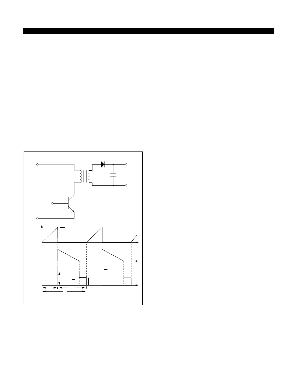
(a) The Buck converter.
The forward converter family which includes thepush-pull
and bridge types, are all based on the buck converter,
shown in Fig. 2. Its operation is straightforward. When
switch TR1 is turned on, the input voltage is applied to
inductor L1 and power is delivered to the output. Inductor
current also builds up according to Faraday’s law shown
below:-
dI
V =L
dt
When the switch is turned off, the voltage across the
inductor reverses and freewheel diode D1 becomes
forwardbiased.Thisallows theenergystoredin theinductor
tobe deliveredto theoutput. Thiscontinuous currentis then
smoothedby outputcapacitor Co. Typical buck waveforms
are also shown in Fig. 2.
toff
T = ton + toff
Vin
Applied
voltage
Inductor
current
Inductor
voltage
TR1
current
v
A
0
I
L
0
V
L
0
Iin
0
ton toff
TR1
CONTROL
CIRCUIT
ton
Vo
Vin
Vin - Vo
Vo
T
Fig. 2 Buck Regulator (step-down).
The LC filter has an averaging effect on the applied
pulsating input, producinga smoothdc output voltageand
current, with very small ripple components superimposed.
The average voltage/sec across the inductor over a
complete switching cycle must equal zero in the steady
state. (The same applies toall ofthe regulatorsthat willbe
discussed.)
L1
D1
Vo
I
D
Continuous mode
Vo
Co
Io
t
t
t
t
108

S.M.P.S. Power Semiconductor Applications
Philips Semiconductors
Neglecting circuit losses, the average voltage at the input
side of the inductor is VinD, while Vois the output side
voltage. Thus, in the steady state, for the average voltage
acrossthe inductor to bezero, the basic dcequation ofthe
buck is simply:-
V
o
= D
V
i
D is the transistor switch duty cycle, defined as the
conduction time divided by one switching period, usually
expressed in the form shownbelow:-
t
on
; where T =t
D =
T
on+toff
Thus,thebuck isa stepdowntype, wherethe outputvoltage
isalwayslower thantheinput.(Since Dnever reachesone.)
Output voltage regulation is provided by varying the duty
cycle of the switch. The LC arrangement provides very
effective filtering of the inductor current. Hence, the buck
and its derivatives all have very low output ripple
characteristics. The buck is normally always operated in
continuous mode ( inductor current never falls to zero)
where peak currents are lower, and the smoothing
capacitor requirements are smaller. There are no major
control problems with the continuous mode buck.
(b) The Boost Converter.
Operation of another fundamental regulator, the boost,
shown in Fig. 3 is more complex than the buck. When the
switch is on,diode D1 is reversebiased, and Vinis applied
across inductor, L1. Current builds up in the inductor to a
peak value, either from zero current in a discontinuous
mode, or an initial value in the continuousmode. When the
switch turns off, the voltage across L1 reverses, causing
thevoltage at the diode to rise above the input voltage.The
diodethen conductsthe energy stored inthe inductor, plus
energy direct from the supply to the smoothing capacitor
and load. Hence, Vois always greater than Vin, making this
a stepup converter. For continuous mode operation, the
boost dc equation is obtained by a similar process as for
the buck, and is givenbelow:-
V
1
o
=
V
1− D
i
Again, the output only depends upon the input and duty
cycle.Thus, by controlling the duty cycle, outputregulation
is achieved.
From the boost waveforms shown in Fig. 3, it is clear that
thecurrent supplied to the output smoothingcapacitor from
the converter is the diode current, which will always be
discontinuous. This means that the output capacitor must
be large, with a low equivalent series resistance (e.s.r) to
produce a relatively acceptable output ripple. This is in
contrast to the buck output capacitor requirements
describedearlier.Ontheother hand,the boostinput current
is the continuous inductor current, and this provides low
input ripple characteristics. The boost is very popular for
capacitive load applications such as photo-flashers and
batterychargers.Furthermore, thecontinuous inputcurrent
makestheboost apopularchoice asapre-regulator,placed
before the main converter. The main functions being to
regulate the input supply, and to greatly improve the line
powerfactor. This requirementhas become very important
in recent years, in a concertedeffort to improve the power
factor of the mains supplies.
TR1
CONTINUOUS MODE
D1
Vo
Co
t
I
in
t
Io
t
t
Vin
TR1
voltage
Inductor
current
Diode
current
TR1
current
V
ce
0
I
L
0
I
D
0
0
Vo
CONTROL
CIRCUIT
Vo
ton toff
T
L1
Fig. 3 Boost Regulator (step-up).
If the boost is used in discontinuous mode, the peak
transistor and diode currentswill behigher, andthe output
capacitor will need to be doubled in size to achieve the
sameoutput rippleas in continuousmode. Furthermore, in
discontinuous operation, the output voltage also becomes
dependent on the load, resulting in poorerload regulation.
Unfortunately, there are major control and regulation
problems with the boost when operated in continuous
mode. The pseudo LC filter effectively causes a complex
second order characteristic in the small signal (control)
response. In the discontinuous mode, the energy in the
inductorat the startof each cycle is zero. Thisremoves the
inductancefrom the small signalresponse, leaving only the
output capacitance effect. This produces a much simpler
response, which is far easierto compensate and control.
109

S.M.P.S. Power Semiconductor Applications
Philips Semiconductors
(c) The Buck-Boost Regulator
(Non-isolated Flyback).
Thevery popular flyback converter(see section 5(a)) is not
actually derived solely from the boost. The flyback only
delivers stored inductor energy during the switch off-time.
The boost, however, also delivers energy from the input.
The flyback is actually based on a combined topology of
the previous two, called the buck-boost or non isolated
flyback regulator. This topology isshown in Fig. 4.
Vin
Vo
TR1
CONTROL
CIRCUIT
Step up / down Polarity inversion
D1
L1
Fig. 4 Buck-Boost (Flyback) Regulator.
When the switch ison, thediode isreverse biased andthe
inputis connectedacrossthe inductor,whichstores energy
as previously explained. At turn-off, the inductor voltage
reverses and the stored energy is then passed to the
capacitor and load through the forward biased rectifier
diode.
-Vo
Co
The waveforms are similar to the boost except that the
transistorswitch now has to support thesum of Vinand Vo
across it. Clearly, both the input and output currents must
be discontinuous. There is also a polarity inversion, the
output voltage generated is negative with respect to the
input. Close inspection reveals that the continuous mode
dc transfer function is asshown below:-
V
D
o
=
V
1− D
i
Observation shows that the value of the switch duty ratio,
D canbe selected such that the output voltage can either
be higher or lower than the input voltage. This gives the
converter the flexibility to either step up or step down the
supply.
Thisregulator also suffers from the same continuous mode
control problems as the boost, and discontinuous modeis
usually favoured.
Since both input and output currents are pulsating, low
ripple levels are very difficult to achieve using the
buck-boost. Very large outputfilter capacitorsare needed,
typically up to 8 timesthat of a buck regulator.
The transistor switch also needs to be ableto conduct the
highpeakcurrent,aswellas supportingthehigher summed
voltage.Theflyback regulator(buck-boost) topologyplaces
the most stress on the transistor. The rectifier diode also
hasto carry high peak currentsandso the r.m.s conduction
losses will be higher thanthose of the buck.
110
S.M.P.S. Power Semiconductor Applications
Philips Semiconductors
(3) Transformers in S.M.P.S. converters.
The non-isolated versions have very limited use, such as
dc-dcregulators onlycapable of producing asingle output.
Theoutput range is also limited by the input and dutycycle.
The addition of a transformer removes most of these
constraints and provides a converter with the following
advantages:-
1) Input to output isolation is provided. This is normally
alwaysnecessaryfor 220/ 110V mainsapplications, where
a degree of safety isprovided for the outputs.
2) The transformer turns ratio can be selected to provide
outputs widely different from the input; non-isolated
versions are limited to a range of approximately 5 times.
By selecting the correct turns ratio, the duty cycle of the
converter can also be optimised and the peak currents
flowing minimised. The polarity of each output is also
selectable, dependent upon the polarity of the secondary
w.r.t the primary.
3) Multiple outputs are very easily obtained, simply by
adding more secondary windings tothe transformer.
There are some disadvantages withtransformers, suchas
theiradditional size,weight and powerloss. Thegeneration
of voltage spikes due to leakageinductance may alsobe a
problem.
Theisolatedconverters tobecovered aresplitintotwo main
categories, called asymmetrical and symmetrical
converters, depending upon how the transformer is
operated.
B
asymmetrical
converters
forward
symmetrical
converters
2Bs
Fig. 5 Comparative core usage of asymmetrical and
symmetrical converters.
converter
symmetrical
converters
available
flux swing
flyback
converter
Bs
H
Inasymmetrical convertersthemagnetic operatingpoint of
the transformer is always in one quadrant i.e the flux and
the magnetic field never changes sign. Thecore has to be
reseteachcycle toavoid saturation, meaning that only half
of the usable flux is ever exploited. This can be seen in
Fig. 5, which shows the operating mode of eachconverter.
The flyback and forward converter are both asymmetrical
types.Thediagramalso indicatesthat theflyback converter
is operated at a lower permeability (B/H) and lower
inductance than the others. This is because the flyback
transformeractuallystoresalloftheenergy beforedumping
into the load, hence an air gap is required to store this
energyand avoidcoresaturation. Theair gap hastheeffect
of reducing the overall permeability of the core. All of the
other converters have true transformer action and ideally
store no energy, hence, noair gap is needed.
Inthesymmetrical converterswhichalways requirean even
number of transistor switches, the full available flux swing
in both quadrants of the B / H loop is used, thus utilising
the core much more effectively. Symmetrical converters
cantherefore producemore power thantheir asymmetrical
cousins. The 3 major symmetrical topologies used in
practiceare thepush-pull, the half-bridgeand thefull bridge
types.
Table 1 outlines the typical maximum output power
available from each topology using present day
technologies:-
Converter Topology Typical max output power
Flyback 200W
Forward 300W
Two transistor forward / 400W
flyback
Push-pull 500W
Half-Bridge 1000W
Full-Bridge >1000W
Table 1. Converter output power range.
Manyother topologies exist, butthe types outlined in Table
1 are by far the most commonly used in present S.M.P.S.
designs. Each is now looked at in more detail, with a
selection guide for the most suitable Philips power
semiconductors included.
111

S.M.P.S. Power Semiconductor Applications
Philips Semiconductors
(4) Selection of the power
semiconductors.
The Power Transistor.
The two mostcommon power semiconductorsused in the
S.M.P.S.arethe Bipolartransistorand thepowerMOSFET.
The Bipolar transistor is normally limited to use at
frequencies up to 30kHz, due to switching loss. However,
it has very low on-state losses and is a relatively cheap
device, making it the most suitable for lower frequency
applications.The MOSFETis selected forhigher frequency
operation because of its very fast switching speeds,
resulting in low (frequency dependent) switching losses.
The driving of the MOSFET is also far simpler and less
expensive than thatrequired for theBipolar. However, the
on-state losses of the MOSFET are far higher than the
Bipolar, and they are also usually more expensive. The
selection of which particular device to use is normally a
compromise between the cost, and the performance
required.
(i) Voltage limiting value:After deciding uponwhether to use a Bipolar orMOSFET,
the next step in deciding upon a suitable type is by the
correct selection of the transistor voltage. For transformer
coupled topologies, the maximum voltage developed
across the device is normally at turn-off.This willbe either
half,fullordoublethemagnitude ofthe inputsupply voltage,
dependent upon the topology used. There may also be a
significant voltage spike due to transformer leakage
inductance that must be included. The transistor must
safely withstand these worst case values withoutbreaking
down. Hence, for a bipolar device, a suitably high V
must be selected, and for a MOSFET, a suitably high
V
.Atpresent 1750V is themaximum blocking voltage
BR(DSS)
available for power Bipolars,and a maximum of 1000V for
power MOSFETs.
The selection guides assume that a rectified220V or 110V
mainsinput is used. The maximum dc link voltages that will
be produced for these conditions are 385V and 190V
respectively.Thesevalues arethe inputvoltage levelsused
to select the correct devicevoltage rating.
(ii) Current limiting value:The Bipolar device has a very low voltage drop across it
during conduction, which is relatively constant within the
rated current range. Hence, for maximum utilisation of a
bipolar transistor, it should be run close to its I
This gives a good compromise between cost, drive
requirements and switching. The maximum current for a
particularthroughputpower iscalculated for each topology
Csat
ces(max)
value.
using simple equations. These equations are listed in the
appropriatesections,andthe levelsobtainedused toselect
a suitable Bipolar device.
The MOSFET device operatesdifferently from the bipolar
in that the voltage developed across it (hence, transistor
dissipation) is dependent upon the current flowingand the
device "on-resistance" which is variable with temperature.
Hence, the optimum MOSFET for a given converter can
onlybechosen onthe basisthatthedevicemust notexceed
a certain percentageof throughput (output) power.(In this
selection a 5% loss in the MOSFET was assumed). A set
of equations used to estimate the correct MOSFET R
DS(on)
valuefor a particular power level has been derived foreach
topology. These equations are included in Appendix A at
the end of the paper. The value of RDS(on) obtained was
then used to select a suitable MOSFET device for each
requirement.
NOTE! This method assumes negligible switching losses
in the MOSFET. However for frequencies above 50kHz,
switching losses become increasingly significant.
Rectifiers
Two types of output rectifier are specified from the Philips
range. For very low output voltages below 10V it is
necessarytohaveanextremely lowrectifierforwardvoltage
drop,VF,inorder tokeep converterefficiency high.Schottky
typesare specifiedhere,since theyhave verylowVFvalues
(typically 0.5V). The Schottky also has negligible switching
losses and can be used at very high frequencies.
Unfortunately,theverylowVFoftheSchottkyis lostathigher
reverseblocking voltages (typicallyabove100V ) and other
diode types become more suitable. This means that the
Schottky is normally reserved for useon outputsup to 20V
or so.
Note. A suitable guideline in selecting the correct rectifier
reversevoltageis toensurethedevice willblock 4to6times
theoutputvoltageitisusedtoprovide(depends ontopology
and whether rugged devices arebeing used).
For higher voltage outputs the most suitable rectifier is the
fastrecovery epitaxial diode (FRED). This device has been
optimised for use in high frequency rectification. Its
characteristics include low VF(approx. 1V) with very fast
and efficient switching characteristics. The FRED has
reverse voltage blocking capabilities up to 800V. They are
therefore suitable for use in outputs from 10 to 200V.
Therectifier devices specified in each selection guide were
chosenashaving thecorrectvoltage limitingvalue andhigh
enoughcurrent handling capability for theparticular output
power specified. (A single outputis assumed).
112
S.M.P.S. Power Semiconductor Applications
Philips Semiconductors
(5) Standard isolated topologies.
(a) The Flyback converter.
Operation
Of all the isolated converters, by far the simplest is the
single-ended flyback converter shown in Fig. 6.The use of
a single transistor switch means that the transformer can
only be driven unipolar (asymmetrical). This results in a
largecore size. The flyback, which is anisolated version of
the buck-boost, does not in truth contain a transformer but
a coupled inductor arrangement. When the transistor is
turned on, current builds up in the primary and energy is
storedin the core, this energy is thenreleased to the output
circuitthroughthe secondary when the switch is turned off.
(A normal transformer such as the types used in the buck
derived topologies couples the energy directly during
transistor on-time, ideally storing noenergy).
D1
TR1
Ip = Vin.ton/Lp
(discontinuous)
n2
T
T1
n:1
Isec = Idiode
leakage
inductance
spike
Vin
Discontinuous
Vin
Primary
current
current
Switch
voltage
sec
I
P
I
sw
0
I
S
I
D
0
Vce
or
Vds
0
Vin + Vo n1
ton toff
Fig. 6 Flyback converter circuit and waveforms.
The polarity of the windings is such that the output diode
blocks during the transistor on time. When the transistor
turns off, the secondary voltage reverses, maintaining a
constant flux in the core and forcing secondary current to
flow through the diode to the output load. The magnitude
Vo
Co
of the peak secondary current is the peak primary current
reached at transistor turn-off reflected through the turns
ratio, thus maintaining a constant Ampere-turn balance.
The fact that all of the output power of the flyback has to
be stored in thecore as 1/2LI2energy means thatthe core
size and cost will be much greater than in the other
topologies, where only the core excitation (magnetisation)
energy, which is normallysmall, isstored. This, in addition
to the initial poor unipolar core utilisation, means that the
transformer bulk is one of the major drawbacks of the
flyback converter.
Inorder toobtain sufficientlyhigh stored energy,theflyback
primary inductance has to be significantly lower than
required for a true transformer, since high peak currents
areneeded. This is normally achieved bygappingthe core.
Thegap reduces the inductance,andmost of thehighpeak
energy is then stored in thegap, thusavoiding transformer
saturation.
When the transistor turns off, the output voltage is back
reflectedthroughthetransformertotheprimaryand inmany
cases this can be nearly as high as the supply voltage.
There is also a voltage spike at turn-off due to the stored
energy in the transformer leakage inductance.This means
that the transistor must be capable of blocking
approximately twice the supply voltage plus the leakage
spike. Hence, for a 220V ac application where the dc link
canbe upto 385V, thetransistor voltage limitingvaluemust
lie between 800 and 1000V.
Using a 1000V Bipolar transistor such as the BUT11A or
BUW13Aallows a switching frequencyof 30kHz to be used
at output powers up to 200Watts.
MOSFETs with 800V and 1000V limiting values can also
beused,suchas theBUK456-800Awhichcansupply100W
t
atswitching frequencies anywhereupto 300kHz.Although
the MOSFET can be switched much faster and has lower
switching losses , it does suffer from significant on-state
t
losses, especially in the higher voltage devices when
compared to the bipolars. Anoutline of suitable transistors
and output rectifiers for different input and power levels
using the flyback is given in Table 2.
t
Onewayofremovingthe transformerleakage voltagespike
is to add a clamp winding as shown in Fig. 8. This allows
the leakage energy to be returned to the input instead of
stressing the transistor. The diode is always placed at the
high voltage end so that the clamp winding capacitance
does not interfere with the transistor turn-oncurrent spike,
whichwould happen if the diode was connected toground.
This clamp is optional and depends on the designer’s
particular requirements.
113
S.M.P.S. Power Semiconductor Applications
Philips Semiconductors
Advantages.
The action of the flyback means that the secondary
inductance is in series with the output diode when current
is delivered to the load; i.e driven from a current source.
This means that no filter inductor is needed in the output
circuit. Hence, each output requires only one diode and
output filter capacitor. This means the flyback is the ideal
choiceforgeneratinglow cost,multipleoutput supplies.The
crossregulationobtained usingmultiple outputsis alsovery
good (load changes on one output have little effect on the
others) because of the absence ofthe output choke, which
degrades this dynamic performance.
Theflybackisalso ideallysuited for generatinghigh voltage
outputs.If a buck type LC filter was used to generate a high
voltage, a very large inductancevalue wouldbe neededto
reduce the ripple current levels sufficiently to achieve the
continuous mode operationrequired. This restriction does
not apply to theflyback, since itdoes notrequire anoutput
inductance for successful operation.
Disadvantages.
From the flyback waveforms in Fig. 6 it is clear that the
output capacitor is only supplied during the transistor off
time. This means that the capacitor has to smooth a
pulsatingoutput current which has higher peak values than
the continuous output current that would be producedin a
forward converter, for example. In order to achieve low
outputripple, very large output capacitorsare needed,with
very low equivalent series resistance (e.s.r). It can be
shown that at the same frequency, an LC filter is
approximately 8 times more effective at ripple reduction
than a capacitor alone. Hence, flybacks have inherently
much higher output ripples than other topologies. This,
togetherwiththe higherpeak currents, largecapacitors and
transformers, limits the flyback to lower output power
applications in the 20 to 200W range. (It should be noted
that at higher voltages, the required output voltage ripple
magnitudes are not normally as stringent, and this means
that the e.s.r requirement andhence capacitor sizewill not
be as large as expected.)
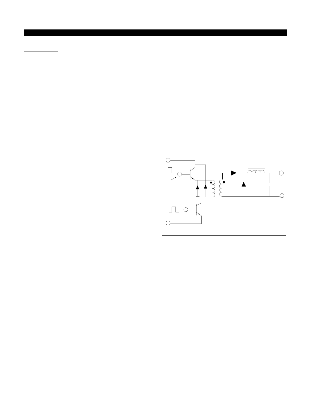
Two transistor flyback.
One possible solution to the 1000V transistor requirement
is the two transistor flyback version shown in Fig. 7. Both
transistorsare switched simultaneously,andall waveforms
are exactly the same, except that the voltageacross each
transistor never exceeds the input voltage. The clamp
winding is now redundant, sincethe two clamp diodes act
to return leakage energy to the input. Two 400 or 500V
devices can now be selected, which will have faster
switching andlower conduction losses. The output power
and switching frequencies can thus be significantly
increased. The drawbacks of the two transistor version are
the extra cost and more complex isolated base drive
needed for the top floating transistor.
Vin
isolated
base
drive
TR2
TR1
T1
n : 1
D1
Fig. 7 Two transistor Flyback.
Continuous Vs Discontinuous operation.
As with the buck-boost, the flyback can operate in both
continuous and discontinuous modes. The waveforms in
Fig. 6 show discontinuous mode operation. In
discontinuous mode, thesecondary current fallsto zero in
each switching period, and all of the energy is removed
from the transformer. In continuous mode there is current
flowing in the coupled inductor at all times, resulting in
trapezoidal current waveforms.
Themain plus of continuous mode is that thepeakcurrents
flowing are only halfthat ofthe discontinuous for the same
output power, hence, lower output ripple is possible.
However, the core size is about 2 to 4 times larger in
continuous mode to achieve the increased inductance
needed to reduce the peakcurrents to achieve continuity.
A further disadvantage of continuous mode is that the
closed loop is far more difficult to control than the
discontinuousmode flyback.(Continuous mode contains a
right hand plane zeroin itsopen loop frequency response,
the discontinuous flyback does not. See Ref[2] for further
explanation.) This means that much more time and effort
is required for continuous mode to design the much more
complicatedcompensationcomponentsneeded toachieve
stability.
There is negligible turn-on dissipation in the transistor in
discontinuous mode, whereas this dissipationcan befairly
high in continuous mode, especially when the additional
effects of the output diodereverse recovery current, which
only occurs in the continuous case, is included. This
normally means that a snubber must be added to protect
the transistor against switch-on stresses.
Oneadvantage ofthe continuous mode isthatits open loop
gain is independentof the output load i.e Voonly depends
uponD and Vinas shown in the dc gainequation at the end
of the section. Continuous mode has excellent open loop
loadregulation, i.e varying the output load will not affect Vo.
Discontinuous mode, on the other-hand, does have a
dependency on theoutput, expressed as RLin the dc gain
equation. Hence, discontinuous mode has a much poorer
114
Vo
Co

S.M.P.S. Power Semiconductor Applications
Philips Semiconductors
openloop loadregulation,i.e changing the outputwill affect
Vo. This problem disappears, however, when the control
loop is closed, and the load regulation problem is usually
completely overcome.
Theuse ofcurrentmode control with discontinuous flyback
(where both the primary current and output voltage are
sensed and combined to control the duty cycle) produces
a much improved overall loop regulation, requiring less
closed loop gain.
Although the discontinuous mode has the major
disadvantageofveryhighpeakcurrentsand alarge output
capacitor requirement, it ismuch easierto implement, and
is by far the more common of the two methods used in
present day designs.
Output power 50W 100W 200W
Line voltage, Vin 110V ac 220V ac 110V ac 220V ac 110V ac 220V ac
Transistor requirements
Max current 2.25A 1.2A 4A 2.5A 8A 4.4A
Max voltage 400V 800V 400V 800V 400V 800V
Bipolar transistors.
TO-220 BUT11 BUX85 BUT12 BUT11A --- BUT12A
Isolated SOT-186 BUT11F BUX85F BUT12F BUT11AF --- BUT12AF
SOT-93 --- --- --- --- BUW13 ---
Isolated SOT-199 --- --- --- --- BUW13F ---
Power MOSFET
TO-220 BUK454-400B BUK454-800A BUK455-400B BUK456-800A --- ---
Isolated SOT-186 BUK444-400B BUK444-800A BUK445-400B BUK446-800A --- ---
SOT-93 --- --- --- --- BUK437-400B BUK438-800A
Output Rectifiers
O/P voltage
5V PBYR1635 PBYR2535CT ---
10V PBYR10100 PBYR20100CT PBYR30100PT
BYW29E-100/150/200 BYV79E-100/150/200 BYV42E-100/150/200
BYV72E-100/150/200
20V PBYR10100 PBYR10100 PBYR20100CT
BYW29E-100/150/200 BYW29E-100/150/200 BYV32E-100/150/200
50V BYV29-300 BYV29-300 BYV29-300
100V BYV29-500 BYV29-500 BYV29-500
Table 2. Recommended Power Semiconductors for single-ended flyback.
Note! The above values are for discontinuous mode. In continuous mode the peak transistor currents are approximately
halved and the output power available is thus increased.
Converter efficiency, η = 80%; Max duty cycle, D
Max transistor voltage, V
Maxtransistorcurrent,IC; ID= 2
dc voltage gain:- (a) continuous (b) Discontinuous
Vin
Vo
= n
D
1− D
or V
= 2V
ce
ds
+ leakage spike
in(max)
η D
max
P
out
maxVmin
= 0.45
Vo
Vin
= D
RLT
2 L
√
P
Applications:- Lowest cost, multiple output supplies in the 20 to 200W range. E.g. mains input T.V. supplies, small
computer supplies, E.H.T. supplies.
115
Flyback

S.M.P.S. Power Semiconductor Applications
Philips Semiconductors
(b) The Forward converter.
Operation.
The forward converter is also a single switch isolated
topology, and is shown inFig. 8. Thisis based onthe buck
converter described earlier, with the addition of a
transformer and another diode in the output circuit. The
characteristic LC output filter isclearly present.
In contrast tothe flyback, the forwardconverter has a true
transformer action, where energyis transferred directly to
the output through the inductor during the transistor
on-time. It can be seen that the polarity of the secondary
winding is opposite to that of the flyback, hence allowing
direct current flow through blocking diode D1. During the
on-time, the current flowing causesenergy to bebuilt up in
the output inductor L1. When the transistor turns off, the
secondary voltage reverses, D1 goes from conducting to
blocking mode and the freewheel diode D2 thenbecomes
forwardbiased and provides a path for theinductor current
to continue to flow. This allows the energy stored in L1 to
be released into the load during the transistor off time.
The forward converter is always operated in continuous
mode (in this case the output inductor current), since this
producesverylowpeak inputand output currentsand small
ripple components. Going into discontinuous mode would
greatly increase these values, as well as increasing the
amountof switching noisegenerated. No destabilising right
hand plane zero occurs in the frequency response of the
forwardin continuous mode (as with thebuck). See Ref[2].
This means thatthe control problemsthat existed with the
continuous flyback are not present here. So there are no
realadvantages to be gained by using discontinuous mode
operation for the forward converter.
Advantages.
As can beseen from the waveforms in Fig. 8, the inductor
current IL, which is also the output current, is always
continuous. The magnitude of the ripple component, and
hence the peak secondary current,depends uponthe size
of the output inductor. Therefore, the ripple can be made
relatively small compared to the output current, with the
peak current minimised. This lowripple, continuousoutput
currentis very easyto smooth, and so the requirements for
the output capacitor size, e.s.r and peak current handling
are far smaller than theyare for the flyback.
Since the transformer in this topology transfers energy
directly there is negligible stored energy in the core
compared to the flyback. However, there is a small
magnetisation energy requiredto excite thecore, allowing
it to become an energy transfer medium. This energy is
very small and only a very small primary magnetisation
current is needed. This means that a high primary
inductance is usually suitable, withno need forthe core air
gap required in the flyback. Standard un-gapped ferrite
cores with high permeabilities (2000-3000) are ideal for
providing the high inductance required. Negligible energy
storage means that the forward converter transformer is
considerablysmaller than the flyback, and core loss is also
muchsmaller forthe samethroughput power. However,the
transformer is still operated asymmetrically, which means
that power is only transferred during the switch on-time,
and this poor utilisation means the transformer is still far
bigger than in the symmetrical types.
The transistors have the same voltage rating as the
discontinuous flyback (see disadvantages), but the peak
current required for the same output power is halved, and
this can be seen in the equations given for the forward
converter. This, coupled with the smaller transformer and
outputfilter capacitorrequirements means that the forward
converter is suitable for use at higher output powers than
the flyback can attain,and is normallydesigned tooperate
inthe 100to 400Wrange. Suitable bipolars and MOSFETs
for the forward converter arelisted in Table 3.
Vin
output
Inductor
current
Diode
currents
TR1
current
Vo
TR1
voltage
Imag
Vce
Clamp
winding
necessary
CONTROL
CIRCUIT
0
I
L
0
Id1
0
0
Ip
0
ton toff
D1
D3
Vin
T1
n : 1
TR1
2Vin
Id2
Id3
Is
T
L1
D2
Vo
Co
t
Io
Fig. 8 The Forward converter and waveforms.
t
t
t
t
116
S.M.P.S. Power Semiconductor Applications
Philips Semiconductors
Disadvantages.
Because of the unipolar switching action of the forward
converter, there is a major problem in how to remove the
core magnetisation energy by the end of each switching
cycle. If this did not happen, there would be a net dc flux
build-up, leadingtocore saturation, and possible transistor
destruction. This magnetisation energy is removed
automatically by the push-pull action of the symmetrical
types. In the flybackthis energy isdumped intothe load at
transistor turn-off. However, there is no such path in the
forward circuit.
Thispath is provided by adding an additionalreset winding
of opposite polarity to the primary. A clampdiode is added,
such that the magnetisation energyis returned to theinput
supply during the transistor off time. The reset winding is
woundbifilarwith the primary to ensure good coupling, and
is normally made tohave thesame numberof turns as the
primary. (The resetwinding wire gauge can be very small,
since it only has to conduct the small magnetisation
current.) The time for the magnetisation energy to fall to
zero is thus the same duration as the transistor on-time.
This means that the maximumtheoretical dutyratio of the
forward converter is 0.5 and after taking into account
switchingdelays,this fallsto 0.45.This limitedcontrol range
isone of the drawbacksof usingthe forward converter. The
waveform of the magnetisation current is also shown in
Fig. 8. The clamp winding in the flyback is optional, but is
always needed in the forwardfor correct operation.
Due to the presence of the reset winding, in order to
maintain volt-sec balancewithin the transformer, the input
voltage is back reflected to the primary from the clamp
winding at transistor turn-off for the duration of the flow of
the magnetisation resetcurrent throughD3. (There is also
a voltage reversal across the secondary winding, and this
is why diode D1 is added to block this voltage from the
output circuit.) This means that the transistor must block
two times Vin during switch-off. The voltage returnsto Vin
after reset has finished, which means transistor turn-on
losses will be smaller. Thetransistors musthave the same
added burden of the voltage rating of the flyback, i.e 400V
for 110V mains and 800Vfor 220V mains applications.
Output diode selection.
The diodes in the output circuit both have to conduct the
full magnitude of the output current. They are also subject
to abrupt changes in current, causing a reverse recovery
spike, particularly in the freewheel diode, D2. This spike
cancauseadditional turn-onswitching lossin thetransistor,
possiblycausing devicefailure in the absence of snubbing.
Thus, very high efficiency, fast trr diodes are required to
minimise conduction losses and to reduce the reverse
recovery spike. These requirements aremet withSchottky
diodes for outputs up to 20V, and fast recovery epitaxial
diodesforhigher voltageoutputs.It isnotnormalfor forward
converter outputs to exceed100V becauseof the need for
a very large output choke, andflybacks arenormally used.
Usually, both rectifiers areincluded ina singlepackage i.e
a dual centre-tap arrangement. The Philips range of
Schottkiesand FREDs which meet these requirements are
also included in Table 3.
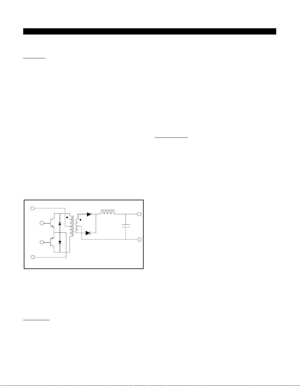
Two transistor forward.
In order to avoid the use of higher voltage transistors, the
two transistor version of the forward can be used. This
circuit, shown in Fig. 9, is very similar to the two transistor
flyback and has the sameadvantages. Thevoltage across
the transistor is again clamped to Vin, allowing the use of
faster more efficient 400 or 500V devices for 220V mains
applications. The magnetisation reset is achieved through
the two clampdiodes, permitting the removalof the clamp
winding.
Vin
L1
isolated
base
drive
TR2
D1
T1
D2
n : 1
TR1
Fig. 9 Two transistor Forward.
The two transistor version is popular for off-line
applications. It provides higher output powers and faster
switching frequencies. The disadvantages are again the
extracost of the higher componentcount, and the needfor
an isolated drive for thetop transistor.
Although this converter has some drawbacks, andutilises
the transformer poorly, itis avery popularselection forthe
power range mentionedabove, and offerssimple drive for
the single switch and cheap component costs. Multiple
output types are very common. The output inductors are
normally wound on a single core, which has the effect of
improving dynamic cross regulation, and if designed
correctly also reduces the output ripple magnitudes even
further. The major advantage of the forward converter is
thevery low output ripple thatcanbe achieved for relatively
small sized LC components. This means that forward
converters are normally used to generate lower voltage,
high current multiple outputs such as 5, 12, 15, 28V from
mains off-line applications, where lower ripple
specifications are normally specified for the outputs. The
high peak currents thatwould occur if a flyback was used
would place an impossible burden on the smoothing
capacitor.
117
Vo
Co

S.M.P.S. Power Semiconductor Applications
Philips Semiconductors
Output power 100W 200W 300W
Line voltage, Vin 110V ac 220V ac 110V ac 220V ac 110V ac 220V ac
Transistor requirements
Max current 2.25A 1.2A 4A 2.5A 6A 3.3A
Max voltage 400V 800V 400V 800V 400V 800V
Bipolar transistors.
TO-220 BUT11 BUX85 BUT12 BUT11A --- BUT12A
Isolated SOT-186 BUT11F BUX85F BUT12F BUT11AF --- BUT12AF
SOT-93 --- --- --- --- BUW13 ---
Isolated SOT-199 --- --- --- --- BUW13F ---
Power MOSFET
TO-220 BUK454-400B BUK454-800A BUK455-400B BUK456-800A --- ---
Isolated SOT-186 BUK444-400B BUK444-800A BUK445-400B BUK446-800A --- ---
SOT-93 --- --- --- --- BUK437-400B BUK438-800A
Output Rectifiers (dual)
O/P voltage
5V PBYR2535CT --- ---
10V PBYR20100CT PBYR30100PT PBYR30100PT
20V PBYR20100CT PBYR20100CT PBYR20100CT
50V BYT28-300 BYT28-300 BYT28-300
BYV32E-100/150/200 BYV42E-100/150/200 BYV72E-100/150/200
BYV72E100/150/200
BYQ28E-100/150/200 BYV32E-100/150/200 BYV32E-100/150/200
Table 3. Recommended Power Semiconductors for single-ended forward.
Forward
Converter efficiency, η = 80%; Max duty cycle, D
Max transistor voltage, V
Maxtransistorcurrent,IC; ID=
dc voltage gain:-
ce
Vo
Vin
or V
= 2V
ds
η D
= nD
max
in(max)
P
out
maxVmin
= 0.45
Applications:- Low cost, low output ripple, multiple output supplies in the 50 to 400W range. E.g. small computer
supplies, DC/DC converters.
118
S.M.P.S. Power Semiconductor Applications
Philips Semiconductors
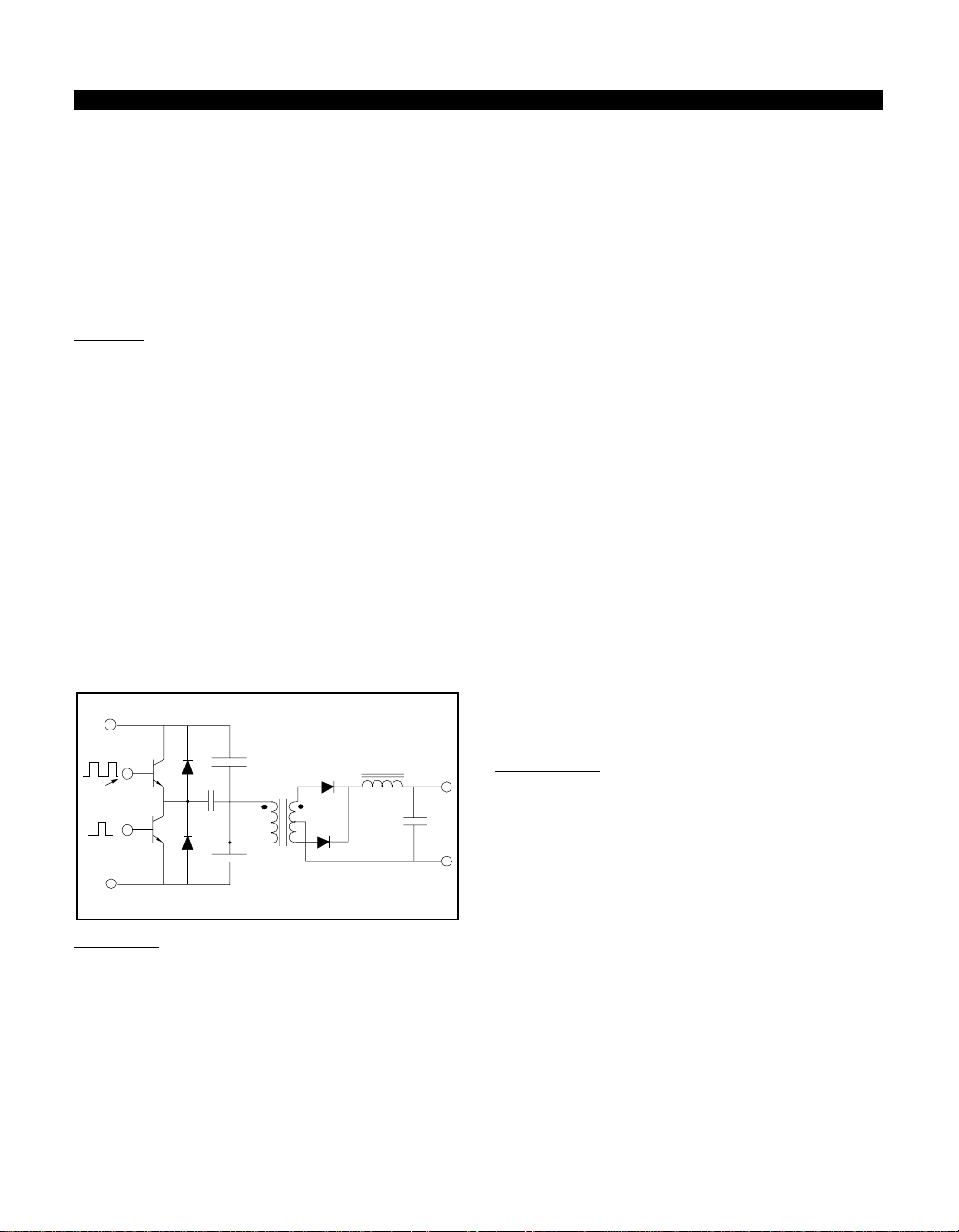
(c) The Push-pull converter.
Operation.
To utilise the transformerflux swingfully, itis necessaryto
operate the core symmetrically as described earlier. This
permits much smaller transformer sizes and provides
higher output powers than possible with the single ended
types. The symmetrical types always require an even
numberof transistor switches. Oneof the best knownofthe
symmetrical types is the push-pull converter shown in
Fig. 10.
The primary is a centre-tapped arrangement and each
transistor switch is driven alternately, driving the
transformerin both directions.The push-pulltransformeris
typically half the size of that for the single ended types,
resulting in a more compact design. This push-pull action
produces natural core resetting during each half cycle,
hence no clamp winding is required. Power is transferred
to the buck type output circuit during each transistor
conduction period. Theduty ratio ofeach switch is usually
less than 0.45. This provides enough dead time to avoid
transistor cross conduction. The power can now be
transferred to the output for up to 90% of the switching
period, hence allowing greaterthroughput power thanwith
the single-ended types. The push-pull configuration is
normally used for output powers in the 100 to500W range.
Vin
TR1
TR2
T1 D1
D2
n : 1
Fig. 10 Push-pull converter.
The bipolar switching action also means that the output
circuitis actually operated at twice the switchingfrequency
ofthepowertransistors, ascanbe seenfromthewaveforms
inFig. 11. Therefore,the outputinductor and capacitor can
be even smaller for similar output ripple levels. Push-pull
converters are thus excellent for high power density, low
ripple outputs.
Advantages.
As stated, the push-pull offers very compact design of the
transformer and output filter, while producing very low
output ripple. So if spaceis a premiumissue, the push-pull
could be suitable. The controlof thepush-pull is similar to
theforward,in thatit isagain basedon thecontinuousmode
L1
Vo
Co
buck. When closing the feedback control loop,
compensation is relatively easy. For multiple outputs, the
same recommendations given for the forward converter
apply.
Clamp diodes are fitted across the transistors, as shown.
Thisallows leakage and magnetisation energytobe simply
channelled back to the supply, reducing stress on the
switches and slightly improving efficiency.
The emitter or source of the power transistors are both at
the same potential in the push-pull configuration, and are
normally referenced to ground. This means that simple
base drive can be used for both, and no costly isolating
drive transformer is required. (Thisis not so for the bridge
types which are discussed latter.)
Disadvantages.
One of the main drawbacks of the push-pull converter is
the fact that each transistor must block twice the input
voltage due to the doubling effect of the centre-tapped
primary,even thoughtwo transistors are used. This occurs
whenonetransistorisoffand theother isconducting. When
both are off, each then blocks the supply voltage, this is
shown in the waveforms in Fig. 11. This means that TWO
expensive,less efficient800 to 1000V transistors would be
required for a 220V off-line application. A selection of
transistors and rectifiers suitable for the push-pull used in
off-line applications is given in Table 4.
Afurther major problem with the push-pull is that it is prone
to flux symmetry imbalance. If the flux swing in each half
cycle is not exactly symmetrical, the volt-sec will not
balance and this will result in transformer saturation,
particularly for high input voltages. Symmetry imbalance
can be caused by different characteristics in the two
transistors such as storage time in a bipolar and different
on-state losses.
The centre-tap arrangement alsomeans that extracopper
isneededforthe primary, and very good coupling between
the two halves is necessary to minimise possible leakage
spikes. It should also benoted that if snubbersare used to
protect the transistors, the design must be very precise
since each tends to interact with the other. This is true for
all symmetrically driven converters.
These disadvantages usually dictate that the push-pull is
normally operated at lower voltage inputs such as 12, 28
or 48V. DC-DC converters found in the automotive and
telecommunication industries are often push-pulldesigns.
At these voltage levels, transformer saturation is easier to
avoid.
Since the push-pull is commonly operated with low dc
voltages,a selectionguide for suitablepower MOSFETs is
alsoincluded for 48 and 96Vapplications, seenin Table 5.
119

S.M.P.S. Power Semiconductor Applications
Philips Semiconductors
Current mode control.
The introduction of current mode control circuits has also
benefited the push-pull type. In this type of control, the
primary current is monitored, and any imbalance which
occursiscorrectedona cycle by cycle basis by varying the
duty cycle immediately. Current mode control completely
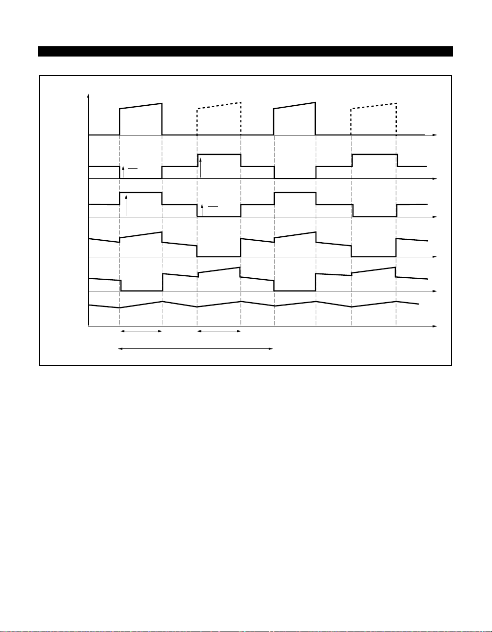
Transistor
currents
TR1
voltage
TR2
voltage
D1
current
D2
current
output
inductor
current
I
TR1
0
0
0
0
0
0
Vin
2Vin
I
L
ton
12
I
TR2
2Vin
Vin
ton
T
Fig. 11 Push Pull waveforms.
removes the symmetry imbalance problem, and the
possibilities of saturation are minimised. This has meant
thatpush-pull designshave becomemore popular inrecent
years, with some designers even using them in off-line
applications.
t
t
t
t
t
t
120

S.M.P.S. Power Semiconductor Applications
Philips Semiconductors
Output power 100W 300W 500W
Line voltage, Vin 110V ac 220V ac 110V ac 220V ac 110V ac 220V ac
Transistor requirements
Max current 1.2A 0.6A 4.8A 3.0A 5.8A 3.1A
Max voltage 400V 800V 400V 800V 400V 800V
Bipolar transistors.
TO-220 BUT11 BUX85 BUT12 BUT11A --- BUT12A
Isolated SOT-186 BUT11F BUX85F BUT12F BUT11AF --- BUT12AF
SOT-93 --- --- --- --- BUW13 ---
Isolated SOT-199 --- --- --- --- BUW13F ---
Power MOSFET
TO-220 BUK454-400B BUK454-800A BUK455-400B BUK456-800A --- ---
Isolated SOT-186 BUK444-400B BUK444-800A BUK445-400B BUK446-800A --- ---
SOT-93 --- --- --- --- BUK437-400B BUK438-800A
Output Rectifiers (dual)
O/P voltage
5V PBYR2535CT --- ---
10V PBYR20100CT PBYR30100PT --20V PBYR20100CT PBYR20100CT PBYR30100PT
50V BYT28-300 BYT28-300 BYV34-300
BYV32E-100/150/200 BYV72E-100/150/200 BYT230PI-200
BYQ28E-100/150/200 BYV32E-100/150/200 BYV42E-100/150/200
BYV72E-100/150/200
Table 4. Recommended Power Semiconductors for off-line Push-pull converter.
Output power 100W 200W 300W
Line voltage, Vin 96V dc 48V dc 96V dc 48V dc 96V dc 48V dc
Power MOSFET
TO-220 BUK455-400B BUK454-200A BUK457-400B BUK456-200B --- ---
Isolated SOT-186 BUK445-400B BUK444-200A BUK437-400B BUK436-200B --- ---
SOT-93 --- --- --- --- BUK437-400B ---
Table 5. Recommended power MOSFETs for lower input voltage push-pull.
Push-Pull converter.
Converter efficiency, η = 80%; Max duty cycle, D
Max transistor voltage, V
Maxtransistorcurrent,IC; ID=
dc voltage gain:-
ce
or V
= 2V
ds
Vo
= 2 nD
Vin
+ leakage spike.
in(max)
P
η D
maxVmin
= 0.9
max
out
Applications:- Compact design, very low output ripple supplies in the 100 to 500W range. More suited to low input
applications. E.g. battery, 28, 40V inputs, high current outputs. Telecommunication supplies.
121
S.M.P.S. Power Semiconductor Applications
Philips Semiconductors
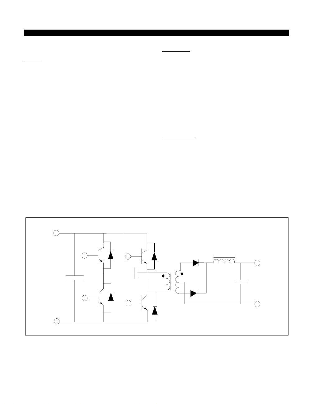
(d) The Half-Bridge.
Of all the symmetrical high power converters, the
half-bridge converter shown inFig. 12 isthe mostpopular.
It is also referred to as the single ended push-pull, and in
principle is a balanced version of the forward converter.
Again it is a derivative of the buck. The Half-Bridge has
some key advantages over the push-pull, which usually
makes it first choice for higher power applications in the
500 to 1000W range.
Operation.
The two mains bulk capacitors C1 and C2 are connected
in series, and an artificial input voltage mid-point is
provided, shown as point A in the diagram. The two
transistorswitches aredriven alternately, andthis connects
eachcapacitor across the single primary windingeach half
cycle. Vin/2 is superimposed symmetrically across the
primaryin a push-pull manner.Power is transferred directly
to the output on each transistor conduction time and a
maximum duty cycle of 90% is available (Some dead time
is required to prevent transistor cross-conduction.) Since
theprimary isdriven in both directions, (naturalreset) a full
wave buck output filter (operating at twice the switching
frequency) rather than a half wave filter is implemented.
This again results in very efficient core utilisation. As can
be seen in Fig. 13, the waveforms are identical to the
push-pull, except that the voltageacross thetransistors is
halved. (The device currentwould be higher for the same
output power.)
Vin
TR1
D3
isolated
drive
needed
D4
TR2
Fig. 12 Half-Bridge converter.
Advantages.
Since both transistors are effectively in series, they never
seegreater than thesupply voltage, Vin.When both are off,
theirvoltages reach anequilibriumpoint of Vin/2.This is half
the voltage rating of the push-pull (although double the
C1
T1
C3
A
C2
D2
n : 1
L1
D1
Vo
Co
current). This means that the half-bridge is particularly
suited to high voltage inputs, such as off-lineapplications.
Forexample, a 220V mains application can use twohigher
speed, higher efficiency 450V transistors instead of the
800V types needed for a push-pull. This allows higher
frequency operation.
Another major advantage over the push-pull is that the
transformer saturation problems due to flux symmetry
imbalance are not a problem. By using a small capacitor
(less than 10µF) any dc build-up of flux in the transformer
isblocked, and onlysymmetrical ac is drawnfrom the input.
The configuration of the half-bridge allowsclamp diodes to
be added across the transistors, shown as D3 and D4 in
Fig. 12. The leakage inductance and magnetisation
energies are dumped straight back into the two input
capacitors, protecting the transistors from dangerous
transients and improving overall efficiency.
A less obvious exclusive advantage of the half-bridge is
that the two series reservoir capacitors already exist, and
this makes it ideal for implementing a voltage doubling
circuit. This permits the useof either110V /220V mainsas
selectable inputs to the supply.
The bridge circuits also have the same advantages over
the single-ended types that the push-pull possesses,
including excellent transformer utilisation, very low output
ripple,andhighoutputpower capabilities.Thelimitingfactor
inthemaximumoutput power availablefrom thehalf-bridge
is the peak current handling capabilities of present day
transistors. 1000W is typically the upper power limit. For
higher output powers thefour switchfull bridgeis normally
used.
Disadvantages.
The need for two 50/60 Hz input capacitors is a drawback
because of their large size. The top transistor must also
have isolated drive, since the gate / base is at a floating
potential. Furthermore, if snubbers are used across the
power transistors, great care must be taken in their design,
since the symmetrical action means that they will interact
with one another. The circuit cost and complexity have
clearlyincreased,and this must be weighed upagainst the
advantagesgained. Inmany cases, this normallyexcludes
the use of the half-bridge at output power levels below
500W.
Suitable transistors and rectifiers for the half-bridge are
given in Table 6.
122
S.M.P.S. Power Semiconductor Applications
Philips Semiconductors
Transistor
currents
TR1
voltage
TR2
voltage
D1
current
D2
current
output
inductor
current
I
TR1
0
Vin
0
0
0
0
0
2
Vin
I
L
ton
12
I
TR2
t
Vin
t
Vin
2
ton
T
t
t
t
t
Fig. 13 Half-Bridge waveforms.
123

S.M.P.S. Power Semiconductor Applications
Philips Semiconductors
Output power 300W 500W 750W
Line voltage, Vin 110V ac 220V ac 110V ac 220V ac 110V ac 220V ac
Transistor requirements
Max current 4.9A 2.66A 11.7A 6.25A 17.5A 9.4A
Max voltage 250V 450V 250V 450V 250V 450V
Bipolar transistors.
TO-220 BUT12 BUT11 --- --- --- ---
Isolated SOT-186 BUT12F BUT11F --- --- --- ---
SOT-93 --- --- BUW13 BUW13 --- BUW13
Isolated SOT-199 --- --- BUW13F BUW13F --- BUW13F
Power MOSFET
SOT-93 --- BUK437-500B --- --- --- ---
Output Rectifiers (dual)
O/P voltage
5V --- --- ---
10V PBYR30100PT --- --20V PBYR20100CT PBYR30100PT ---
50V BYT28-300 BYV34-300 BYV34-300
BYV72E-100/150/200
BYV32E-100/150/200 BYV42E-100/150/200
BYV72E-100/150/200
Table 6. Recommended Power Semiconductors for off-line Half-Bridge converter.
Half-Bridge converter.
Converter efficiency, η = 80%; Max duty cycle, D
Max transistor voltage, V
Maxtransistorcurrent,IC; ID= 2
dc voltage gain:-
ce
or V
ds
= V
Vo
Vin
in(max)
η D
= nD
+ leakage spike.
max
P
out
maxVmin
= 0.9
Applications:- High power, up to 1000W. High current, very low output ripple outputs. Well suited for high input
voltage applications. E.g. 110, 220, 440V mains. E.g. Large computer supplies, Lab equipment supplies.
124
S.M.P.S. Power Semiconductor Applications
Philips Semiconductors
(e) The Full-Bridge.
Outline.
The Full-Bridge converter shown in Fig. 14 is a higher
power version of theHalf-Bridge, andprovides thehighest
output power level of anyof the convertersdiscussed. The
maximum current ratings of the power transistors will
eventually determine the upperlimit ofthe outputpower of
the half-bridge. These levels can be doubled by using the
Full-Bridge, which is obtained by adding another two
transistors and clamp diodes to the Half-Bridge
arrangement.Thetransistors are drivenalternately inpairs,
T1and T3, then T2 and T4. The transformer primary isnow
subjectedtothe fullinputvoltage. Thecurrent levelsflowing
are halved compared to the half-bridge for a given power
level. Hence, the Full-Bridge will double the output power
of the Half-Bridge using the same transistor types.
Thesecondary circuit operates inexactly the samemanner
as the push-pull and half-bridge, also producing very low
ripple outputs at very high current levels. Therefore, the
waveforms for the Full-Bridge are identical to the
Half-Bridge waveforms shown in Fig. 13, except for the
voltage across the primary, which is effectively doubled
(and switch currents halved). This is expressed in the dc
gain and peak current equations, where the factor of two
comes in, compared with the Half-Bridge.
Vin
Advantages.
As stated,the Full-Bridge is ideal for thegeneration of very
high output powerlevels. The increased circuit complexity
normally means that the Full-Bridge is reserved for
applications with power output levels of 1kW and above.
For such high power requirements, designers often select
power Darlingtons, since theirsuperior currentratings and
switching characteristics provide additional performance
and in many cases amore cost effective design.
The Full-Bridge also has the advantage of only requiring
one mains smoothing capacitor compared to two for the
Half-Bridge, hence, saving space. Its other major
advantages are the same asfor the Half-Bridge.
Disadvantages.
Four transistors and clamp diodes are needed instead of
two for the other symmetrical types. Isolated drive for two
floating potential transistors is now required. The
Full-Bridge has the most complex andcostly designof any
oftheconverters discussed,andshould onlybe usedwhere
other types do not meet the requirements. Again, the four
transistor snubbers (if required) must be implemented
carefully to prevent interactions occurringbetween them.
Table 7 gives an outline of the Philips power
semiconductors suitable for use with the Full-Bridge.
C1
* Isolated drive required.
TR1
*
TR2
D3
D4
TR4
*
C2
TR3
D5
D6
D1
T1
D2
L1
Vo
Co
Fig. 14 The Full-Bridge converter.
125

S.M.P.S. Power Semiconductor Applications
Philips Semiconductors
Output power 500W 1000W 2000W
Line voltage, Vin 110V ac 220V ac 110V ac 220V ac 110V ac 220V ac
Transistor requirements
Max current 5.7A 3.1A 11.5A 6.25A 23.0A 12.5A
Max voltage 250V 450V 250V 450V 250V 450V
Bipolar transistors.
TO-220 BUT12 BUT18 --- --- --- ---
Isolated SOT-186 BUT12F BUT18F --- --- --- ---
SOT-93 --- --- BUW13 BUW13 --- BUW13
Isolated SOT-199 --- --- BUW13F BUW13F --- BUW13F
Power MOSFET
SOT-93 --- BUK438-500B --- --- --- ---
Output Rectifiers (dual)
O/P voltage
5V --- --- --10V --- --- --20V PBYR30100PT --- ---
50V BYV34-300 BYV44-300 ---
Table 7. Recommended Power Semiconductors for the Full-Bridge converter.
BYV42E-100/150/200
BYV72E-100/150/200
Converter efficiency, η = 80%; Max duty cycle, D
Max transistor voltage, V
Maxtransistorcurrent,IC; ID=
dc voltage gain:-
ce
or V
= V
ds
in(max)
Vo
= 2 nD
Vin
+ leakage spike.
P
η D
maxVmin
= 0.9
max
out
Applications:- Very high power, normally above 1000W. Very high current, very low ripple outputs. Well suited for
high input voltage applications. E.g. 110, 220, 440V mains. E.g. Computer Mainframe supplies, Large lab equipment
supplies, Telecomm systems.
Full-Bridge converter.
126

S.M.P.S. Power Semiconductor Applications
Philips Semiconductors
Conclusion.
The 5 most common S.M.P.S. converter topologies, the
flyback,forward,push-pull,half-bridgeand full-bridgetypes
have been outlined. Each has its own particular operating
characteristics and advantages, which makes it suited to
particular applications.
Theconvertertopologyalsodefinesthevoltageand current
requirements of the power transistors (either MOSFET or
Bipolar).Simpleequations andcalculations used to outline
the requirements ofthe transistors foreach topology have
been presented.
The selection guide fortransistors andrectifiers atthe end
ofeach topologysectionshows some of thePhilips devices
which are ideal for usein S.M.P.S. applications.
References.
(1) Philips MOSFET Selection Guide For S.M.P.S. by
M.J.Humphreys. Philips Power Semiconductor
Applications group, Hazel Grove.
(2) Switch Mode Power Conversion - Basic theory and
design by K.Kit.Sum. (Published by Marcel Dekker
inc.1984)
127
S.M.P.S. Power Semiconductor Applications
Philips Semiconductors
Appendix A.
MOSFET throughput power calculations.
Assumptions made:The power loss (Watts) in the transistor due to on-state
losses is 5% of the total throughput (output) power.
Switching losses in the transistor are negligible. N.B. At
frequencies significantly higher than 50kHz the switching
losses may become important.
The device junction temperature, Tjis taken to be 125˚C.
Theratio R
ds(125C˚)/Rds(25˚C)
MOSFET device. Table A1 gives the ratio for the relevant
voltage limiting values.
The value of V
A2.
s(min)
Device voltage limiting R
value. --------
100 1.74
200 1.91
400 1.98
500 2.01
800 2.11
1000 2.15
Table A1. On resistance ratio.
Main input Maximum dc link Minimum dc
voltage voltage link
220 / 240V ac 385V 200V
110 / 120V ac 190V 110V
Table A2. Max and Min dc link voltages for mains inputs.
isdependent on thevoltage of the
for each input value is given in Table
ds(125C)
R
ds(25C)
voltage
Using the following equations, for a given device with a
known R
topology can be calculated.
, the maximum throughput power in each
ds(125˚C)
Where:-
P
= Maximum throughput power.
th(max)
D
= maximum duty cycle.
τ = required transistor efficiency (0.05 ± 0.005)
max
Rds
V
s(min)
= R
(125˚C)
= minimum dc link voltage.
ds(25˚C)
x ratio.
Forward converter.
2
τ×V
×D
s(min)
P
th(max)
D
=
max
= 0.45
R
max
ds(125c)
Flyback Converter.
P
th(max)
3×τ×V
=
D
max
s(min)
4× R
= 0.45
ds(125c)
×D
max
2
Push Pull Converter.
2
τ×V
×D
s(min)
P
th(max)
=
D
= 0.9
max
R
max
ds(125c)
Half Bridge Converter.
2
τ×V
×D
s(min)
P
th(max)
=
4× R
D
= 0.9
max
max
ds(125c)
Full Bridge Converter.
2
τ×V
×D
s(min)
P
th(max)
=
2× R
D
= 0.9
max
max
ds(125c)
128

S.M.P.S. Power Semiconductor Applications
Philips Semiconductors
2.1.2 The Power Supply Designer’s Guide to High Voltage
Transistors
One of the most critical components in power switching
converters is the high voltage transistor. Despite its wide
usage, feedback from power supply designers suggests
that there are several features of high voltage transistors
which are generally not wellunderstood.
This section begins with a straightforward explanation of
the key properties of high voltage transistors. This isdone
byshowing howthe basic technology ofthe transistor leads
toits voltage,current,power and secondbreakdownlimits.
It is also made clear how deviations from conditions
specifiedin thedata book will affect the performance of the
transistor. The final section of the paper gives practical
advicefordesignerson howcircuits mightbe optimisedand
transistor failures avoided.
Introduction
A large amount of useful information about the
characteristics of a given component is provided in the
relevant data book. By using this information, a designer
can usually be sure of choosing the optimum component
for a particular application.
However,if aproblem ariseswiththe completedcircuit, and
a more detailed analysis of the most critical components
becomes necessary, the databook can become a source
of frustration rather than practical assistance. In the data
book,a component is often measured under averyspecific
setofconditions.Very littleissaidabouthowthe component
performance is affected if these conditions are not
reproducedexactlywhenthecomponent isused ina circuit.
There are as many different sets of requirements for high
voltage transistors asthere arecircuits whichmake use of
them. Covering every possible drive and load condition in
the device specification is an impossible task. There is
therefore a real need for any designer using high voltage
transistorstohave anunderstandingof howdeviations from
theconditionsspecified inthe transistordatabook willaffect
the electrical performance of the device, in particular its
limiting values.
Feedbackfrom designersimpliesthatthis informationis not
readily available. The intentionof thisreport istherefore to
provide designers with the information they need in order
tooptimise thereliability oftheir circuits.The characteristics
ofhigh voltage transistors stem from their basic technology
and so it is importantto begin with an overview of this.
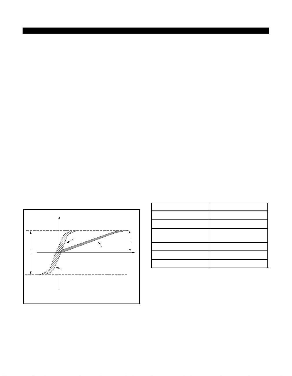
HVT technology
Stripping away the encapsulationof the transistor reveals
how the electrical connections are made (see Fig. 1). The
collector is contacted through the back surface of the
transistorchip,which issolderedtothenickel-plated copper
lead frame. For Philips power transistors the lead frame
andthe centreleg are formed froma single pieceof copper,
and so the collector can be accessed through either the
centre leg or any exposed part of the lead frame (eg the
mounting base for TO-220 and SOT-93).
nickel-plated
copper lead
frame
passivated
chip
aluminium
wires
tinned copper
leads
Base Collector Emitter
Fig. 1 High voltage transistor without the plastic case.
The emitter area ofthe transistor is contactedfrom thetop
surfaceof the chip. A thinlayer of aluminium joinsall of the
emitterareatoalarge bondpad.This bondpadisaluminium
wire bonded to the emitter leg of the transistor when the
transistor is assembled. The same method is used to
contactthe base area of the chip. Fig. 2 shows the top view
of a high voltage transistor chip in more detail.
Viewing thetop surface of the transistor chip,the base and
emitter fingers are clearly visible. Around the periphery of
the chip is the high voltageglass passivation. The purpose
of this is explained later.
Taking across section through the transistor chip reveals
its npn structure. A cross section which cuts one of the
emitterfingersandtwoofthebasefingersisshowninFig. 3.
ultrasonic
wire bonds
129

S.M.P.S. Power Semiconductor Applications
Philips Semiconductors
Following the collector regionis the n+ backdiffusion. The
n+back diffusion ensures a goodelectrical contactismade
between the collector region and the lead frame/collector
base
bond pad
emitter
bond pad
leg, whilst also allowing the crystal to be thick enough to
prevent it from cracking during processing and assembly.
Thebottomsurfaceofthechip issoldered tothe leadframe.
Voltage limiting values
Part 1: Base shorted to emitter.
high
voltage
passivation
emitter fingersbase fingers
Fig. 2 High voltage transistor chip.
When the transistor is in its off state with a high voltage
applied to the collector, the base collector junction is
reverse biased by a very high voltage. The voltage
supporting
depletionregion
extendsdeep intothe collector,
right up to the backdiffusion, as shown in Fig. 4.
base finger emitter finger base finger
Onthe topsurfaceofthe transistorare thealuminium tracks
whichcontactthebase andemitterareas. Theemitterfinger
isshownconnectedtoan n+region. Thisis theemitter area.
Then+ denotes thatthis is very highly doped n type silicon.
Surrounding the n+ emitter is the base, and as shown in
Fig. 3 this is contacted by the base fingers, one on either
side of theemitter. The p denotesthat thisis highly doped
p type silicon.
Onthe other side of the base isthethick collectorn-region.
The n- denotes that this is lightly dopedn type silicon.The
collector region supports the transistor blocking voltage,
and its thickness and resistivity must increase with the
voltage rating of the device.
base finger emitter finger base finger
base
collector
back diffusion
solder
lead frame
emitter
n+
p
n-
n+
Fig. 3 Cross section of HVT.
base
emitter
n+
p
Depletion Region
collector
back diffusion
Fig. 4 Depletion region extends deep into the collector
during the off state.
Withthe base of the transistor short circuited to the emitter,
or at a lower potential than the emitter, the voltage rating
is governed by the voltage supporting capability of the
reversebiased basecollector junction. This isthe transistor
V
.Thebreakdownvoltage ofthereversebiasedbase
CESMmax
collectorjunctionisdetermined mainlybythe collectorwidth
and resistivity as follows:
Figure5 shows the doping profile of the transistor.Notethe
very high doping of the emitter and the back diffusion, the
highdopingof the base and the low doping of the collector.
Also shown in Fig. 5 is the electric field concentration
throughout the depletion region for the case where the
transistor is supporting its off state voltage. The electric
field, E, is given bythe equation, E = -dV/dx, where -dV is
the voltage drop in a distance dx. Rewriting this equation
gives the voltage supported by the depletion region:
V =−
n-
n+
⌠
Edx
⌡
130

S.M.P.S. Power Semiconductor Applications
Philips Semiconductors
avoided by the use ofa glasspassivation (see Fig. 6).The
Doping
E field
glasspassivation therefore allowsthe full voltage capability
of the transistor to berealised.
n+
n+
p
n-
EB C
Distance
Fig. 5 Doping profile and E field distribution.
This is the area underthe dotted line in Fig.5.
During the off state, the peak electric field occurs at the
basecollectorjunctionasshownin Fig. 5.If theelectric field
anywherein thetransistor exceeds 200 kVoltsper cm then
avalanche breakdown occurs and the current which flows
in the transistor is limited only by the surrounding circuitry.
If the avalanche current is not limited to a very low value
then the power rating of the transistor can easily be
exceededandthetransistordestroyedas aresultofthermal
breakdown. Thus the maximum allowable value ofelectric
field is 200 kV/cm.
The gradient of the electric field, dE/dx, is proportional to
charge densitywhich is in turn proportional to the level of
doping. In the base, thegradient ofthe electricfield ishigh
because of the high level of doping, and positivebecause
the base is p type silicon. In the collector, the gradient of
the electric field is low because of the low level of doping,
and negative becausethe collector isn type silicon. In the
backdiffused region, the gradient ofthe electric field is very
highly negative because this is very highly doped n type
silicon.
Increasing the voltage capability of the transistor can
therefore be done by either increasing the resistivity
(loweringthe level of doping) of thecollector region in order
tomaintain a high electric field for the entire collectorwidth,
or increasing the collector width itself. Both of these
measures can be seen to work in principle because they
increase the area under thedotted line in Fig. 5.
Thebreakdown voltage of the transistor, V
CESMmax
,is limited
by the need to keep the peak electric field, E, below 200
kV/cm. Without special measures, the electric field would
crowd at the edges of the transistor chip because of the
surface irregularities. Thiswould limit breakdown voltages
to considerably less than the full capability of the silicon.
Crowding of the equipotential lines at the chip edges is
emitter
n+
250V
600V
850V
1150V
n+
n-
n+
special glass
base
p
n-
Fig. 6 High voltage passivation.
Theglassusedisnegatively charged toinduce ap-channel
underneath it. This ensures that the applied voltage is
supported evenly over the width ofthe glass and does not
crowd at any one point. High voltagebreakdown therefore
occurs in the bulk of the transistor, at the base collector
junction, and not at the edges of the crystal.
Exceeding the voltage rating of the transistor, even for a
fraction of a second, must be avoided. High voltage
breakdowneffectscanbe concentratedin a verysmall area
of the transistor, and only a small amount of energy may
damage the device. However,there is no danger in using
thefull voltagecapability of thetransistor asthe limit under
worstcase conditionsbecause thehigh voltagepassivation
is extremely stable.
Part 2: Open circuit base.
With the base of the transistor open circuit the voltage
capability is much lower. This is the V
and it is typically just less than half of the V
The reason for the lower voltage capability under open
CEOmax
of the device
rating.
CESMmax
circuit base conditions is asfollows:
As the collector emitter voltage of the transistor rises, the
peakelectricfield locatedat thebasecollector junctionrises
too. Above a peak E field value of 100 kV/cm there is an
appreciable leakage current being generated.
In the previous case, with the base contact shortcircuited
to the emitter,or held at a lower potential thanthe emitter,
any holes which are generated drift from the edge of the
depletion region towards the base contact where they are
extracted.However, withthe base contact opencircuit, the
holes generated diffuse from the edge of the depletion
region towards the emitter where they effectively act as
basecurrent.Thiscauses theemitterto injectelectrons into
thebase, whichdiffuse towards the collector.Thus there is
a flow of electrons from the emitter to the collector.
131

S.M.P.S. Power Semiconductor Applications
Philips Semiconductors
The high electric field in the collector accelerates the
electronstothe level where some have sufficient energy to
produce more hole electron pairs through their collisions
with the lattice. The current generated in this way adds to
theleakagecurrent.Thus withthebase contactopen circuit
the emitter becomes active and provides the system with
gain
, multiplying the leakage current and consequently
reducing the breakdown voltage.
For a given transistor the gain of the system is dependant
on two things. Firstlyit is dependant on theprobability that
a hole leaving thedepletion regionwill reachthe emitter.If
the base isopen circuit andno recombination occurs then
this probability is 1. If the base is not open circuit, and
instead a potential below V
is applied, then there is a
BEon
chance that a hole leaving the depletion region will be
extracted atthe base contact. As the voltage on the base
contact is made less positive the probability of holes
reaching the emitter is reduced.
Secondly, the gain is dependant on the probability of
electronsleavingthe emitter, diffusing across the base and
being accelerated by the high field in the collector to the
level where they are able toproduce ahole electron pair in
one of their collisions with thelattice. This depends on the
electric field strength which is in turn dependant on the
collector voltage.
Thusforagiven voltageatthe basethereis acorresponding
maximum collector voltage before breakdown will occur.
With the base contact shorted to the emitter, or at a lower
potentialthan the emitter, the full breakdown voltage ofthe
transistorisachieved(V
circuit, or at a
higher
breakdown voltage is lower (V
the emitter is active and it provides the breakdown
).Withthebasecontactopen
CESMmax
potential than the emitter, the
) because in this case
CEOmax
mechanism with gain.
With the base connected to the emitter by a non zero
impedance, the breakdown voltage will be somewhere
between the V
CESMmax
and the V
. A low impedance
CEOmax
approximates to the shorted base, ’zero gain’, case and a
highimpedanceapproximates tothe openbase, ’highgain’,
case. With a base emitter impedance of 47 Ω and no
externally applied base voltage, the breakdown voltage is
typically 10% higher than theV
CEOmax
.
Current limiting values
The maximum allowed DC current is limited by the size of
the bond wires to the baseand emitter. Exceeding the DC
limiting values I
time, may blowthese bond wires. If the current pulses are
short and of alow duty cycle then valuesgreatly in excess
of the DC values areallowed. The I
are recommendations for peak current values. For a duty
cycle of 0.01 and a pulse width of 10ms these values will
typically be double the DCvalues.
Cmax
and I
, for any significant length of
Bmax
and I
CMmax
BMmax
ratings
If the pulses are shorter than 10ms then even the
recommended peak values can be exceeded under worst
case conditions. However, it should be noted that
combinations of high collector current and high collector
voltagecanleadtofailureby secondbreakdown(discussed
later). As the collector current is increased, the collector
voltage required to trigger second breakdown drops, and
soallowinglarge collector current spikes increasesthe risk
of failure by second breakdown. It istherefore advised that
the peak values givenin thedata bookare used as design
limits in order to maximisethe component reliability.
In emitter drive circuits, the peak reverse base current is
equal to the peak collector current. The pulse widths and
duty cycles involvedare small, and this modeof operation
iswithin the capability of all Philips high voltage transistors.
Power limiting value
The P
achievable parameter because in practice it is obtainable
onlyif the mountingbasetemperature can be held to25 ˚C.
In practice, themaximum power dissipation capability of a
givendevice is limited by the heatsink size and theambient
temperature.Themaximumpowerdissipation capabilityfor
a particular circuit can becalculated as follows;
T
jmax
sheet. The value normally quoted is 150 ˚C. T
ambient temperature around the device heatsink.A typical
valuein practice could be 65˚C. R
resistance given inthe data sheet, but to obtain a value of
junction to
resistance of the mica spacer (if used), heatsink and
heatsink compound should be added to this.
Themaximumpower whichcanbedissipatedunderagiven
set of circuit conditions iscalculated using;
For a BUT11AF, in an ambient temperature of 65 ˚C,
mounted on a 10 K/W heatsink with heatsink compound,
this gives;
andhencethemaximumpowercapable ofbeing dissipated
under these conditions is;
Exceeding the maximum junction temperature,T
recommended. All of the quality andreliability work carried
out on the device is based on the maximum junction
temperaturequoted indata. IfT
then the reliability of the device is no longer guaranteed.
given in device data is not generally an
totmax
isthemaximum junction temperature given in the data
is the
amb
isthedevice thermal
thj-mb
ambient
R
thj-a
thermal resistance, R
P
max
= (T
jmax-Tamb
)/R
thj-a
, the thermal
thj-a
= 3.95 K/W + 10 K/W = 13.95 K/W
P
= (150-65)/13.95 = 6 W
max
isexceeded inthe circuit
jmax
jmax
, is not
132
 Loading...