

Philips PMST5550, PMST5551 Datasheet
DISCRETE SEMICONDUCTORS
DATA SH EET
ook, halfpage
M3D187
PMST5550; PMST5551
NPN high-voltage transistors
Product specification
Supersedes data of 1997 May 20
1999 Apr 29
Philips Semiconductors Product specification
NPN high-voltage transistors PMST5550; PMST5551
FEATURES
• Low current (max. 300 mA)
• High voltage (max. 160 V).
APPLICATIONS
• Switching and amplification in high voltage applications
such as telephony.
DESCRIPTION
NPN high-voltage transistor in a SOT323 plastic package.
PNP complement: PMST5401.
MARKING
TYPE NUMBER MARKING CODE
(1)
PMST5550 ∗1F
PMST5551 ∗G3
Note
1. ∗ = - : Made in Hong Kong.
∗ = t : Made in Malaysia.
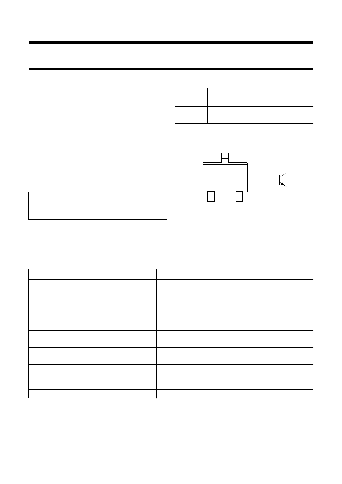
PINNING
PIN DESCRIPTION
1 base
2 emitter
3 collector
handbook, halfpage
Top view
3
1
1
2
MAM062
Fig.1 Simplified outline (SOT323) and symbol.
3
2
LIMITING VALUES
In accordance with the Absolute Maximum Rating System (IEC 134).
SYMBOL PARAMETER CONDITIONS MIN. MAX. UNIT
V
CBO
collector-base voltage open emitter
PMST5550 − 160 V
PMST5551 − 180 V
V
CEO
collector-emitter voltage open base
PMST5550 − 140 V
PMST5551 − 160 V
V
EBO
I
C
I
CM
I
BM
P
tot
T
stg
T
j
T
amb
emitter-base voltage open collector − 6V
collector current (DC) − 300 mA
peak collector current − 600 mA
peak base current − 100 mA
total power dissipation T
≤ 25 °C; note 1 − 200 mW
amb
storage temperature −65 +150 °C
junction temperature − 150 °C
operating ambient temperature −65 +150 °C
Note
1. Transistor mounted on an FR4 printed-circuit board.
1999 Apr 29 2

Philips Semiconductors Product specification
NPN high-voltage transistors PMST5550; PMST5551
THERMAL CHARACTERISTICS
SYMBOL PARAMETER CONDITIONS VALUE UNIT
R
th j-a
Note
1. Transistor mounted on an FR4 printed-circuit board.
CHARACTERISTICS
=25°C unless otherwise specified.
T
amb
SYMBOL PARAMETER CONDITIONS MIN. MAX. UNIT
I
CBO
I
EBO
h
FE
V
CEsat
V
BEsat
C
c
C
e
f
T
F noise figure I
thermal resistance from junction to ambient note 1 625 K/W
collector cut-off current IE= 0; VCB= 100 V − 100 nA
PMST5550 I
collector cut-off current I
PMST5551 I
= 0; VCB= 100 V; T
E
= 0; VCB= 120 V − 50 nA
E
= 0; VCB= 120 V; T
E
= 100 °C − 100 µA
amb
= 100 °C − 50 µA
amb
emitter cut-off current IC= 0; VEB=4V − 50 nA
DC current gain VCE= 5 V; (see Fig.2)
PMST5550 I
DC current gain V
PMST5551 I
collector-emitter saturation
= 1 mA 60 −
C
I
= 10 mA 60 250
C
I
= 50 mA; note 1 20 −
C
= 5 V; (see Fig.2)
CE
= 1 mA 80 −
C
I
= 10 mA 80 250
C
I
= 50 mA; note 1 30 −
C
IC= 10 mA; IB=1mA − 150 mV
voltage
collector-emitter saturation
I
= 50 mA; IB= 5 mA; note 1
C
voltage
PMST5550 − 250 mV
PMST5551 − 200 mV
base-emitter saturation voltage IC= 10 mA; IB=1mA − 1V
base-emitter saturation voltage I
= 50 mA; IB= 5 mA; note 1
C
PMST5550 − 1.2 V
PMST5551 − 1V
collector capacitance IE=ie= 0; VCB= 10 V; f = 1 MHz − 6pF
emitter capacitance IC=ic= 0; VEB= 0.5 V; f = 1 MHz − 30 pF
transition frequency IC= 10 mA; VCE= 10 V; f = 100 MHz 100 300 MHz
= 200 µA; VCE=5V; RS=2kΩ;
C
PMST5551 − 8dB
f = 10 Hz to 15.7 kHz
Note
1. Pulse test: t
≤ 300 µs; δ≤0.02.
p
1999 Apr 29 3
 Loading...