

Page 1
PMK30EP
P-channel TrenchMOS extremely low level FET
Rev. 04 — 25 October 2010 Product data sheet
1. Product profile
1.1 General description
Extremely low level P-channel enhancement mode Field-Effect Transistor (FET) in a
plastic package using TrenchMOS technology. This product is designed and qualified for
use in computing, communications, consumer and industrial applications only.
1.2 Features and benefits
Low conduction losses due to low
1.3 Applications
on-state resistance
Battery management Load switching
1.4 Quick reference data
Table 1. Quick reference data
Symbol Parameter Conditions Min Typ Max Unit
V
DS
I
D
P
tot
Static characteristics
R
DSon
Dynamic characteristics
Q
GD
drain-source voltage 25 °C ≤ Tj≤ 150 °C - - -30 V
drain current Tsp=25°C; VGS=-10V;
see Figure 1; see Figure 3
total power dissipation Tsp=25°C; see Figure 2 --6.9W
drain-source on-state
resistance
gate-drain charge VGS=-10V; ID=-9.2A;
VGS=-10V; ID=-9.2A;
Tj=25°C; see Figure 9
=-15V; Tj=25°C;
V
DS
see Figure 11
; see Figure 12
---14.9A
- 1619mΩ
-7-nC
Page 2
NXP Semiconductors
5
2. Pinning information
PMK30EP
P-channel TrenchMOS extremely low level FET
Table 2. Pinning information
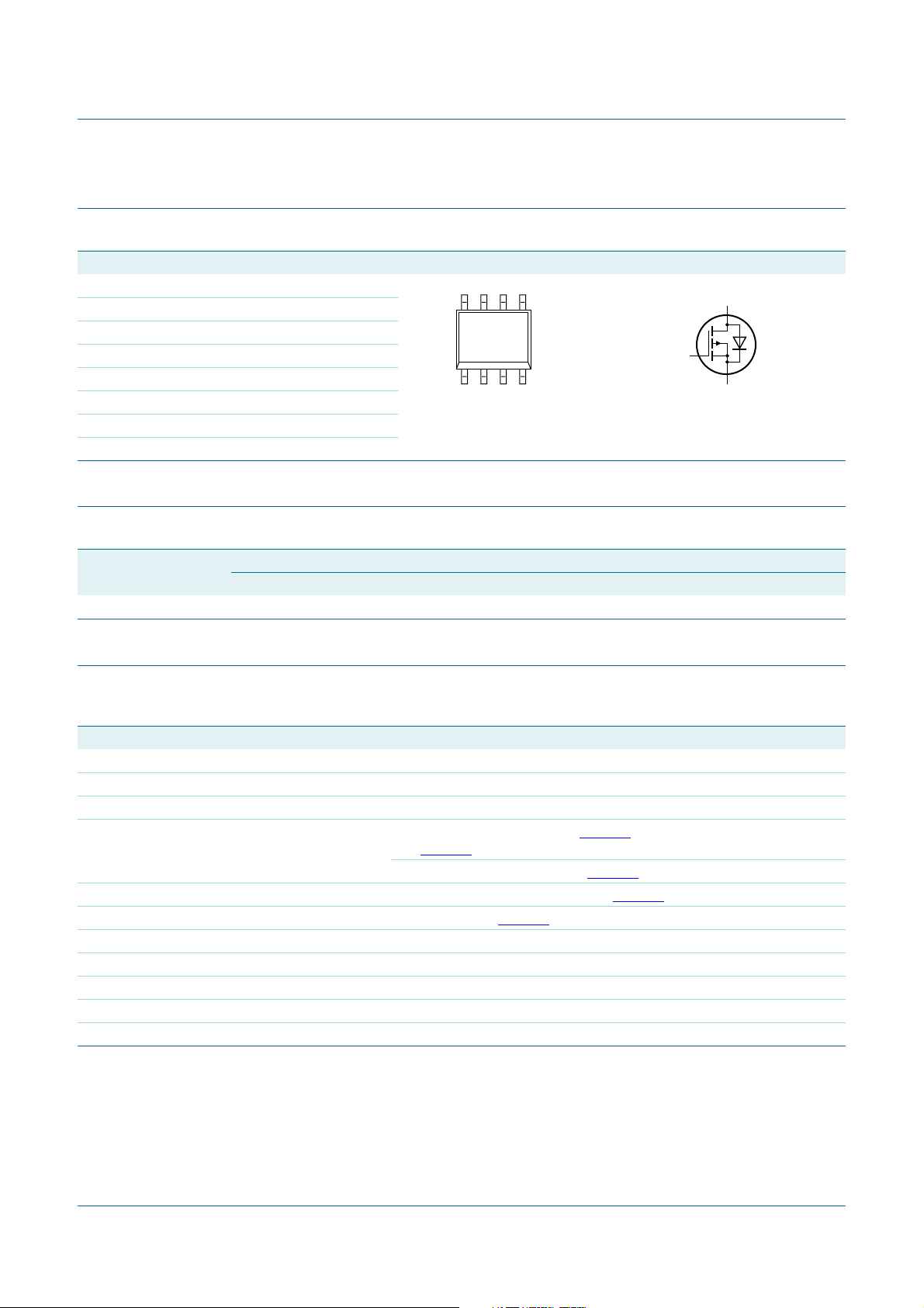
Pin Symbol Description Simplified outline Graphic symbol
1Ssource
2Ssource
8
5
D
3Ssource
4 G gate
5 D drain
6 D drain
1
SOT96-1 (SO8)
4
G
S
001aaa02
7 D drain
8 D drain
3. Ordering information
Table 3. Ordering information
Type number Package
PMK30EP SO8 plastic small outline package; 8 leads; body width 3.9 mm SOT96-1
Name Description Version
4. Limiting values
Table 4. Limiting values
In accordance with the Absolute Maximum Rating System (IEC 60134).
Symbol Parameter Conditions Min Max Unit
V
DS
V
DGR
V
GS
I
D
I
DM
P
tot
T
stg
T
j
Source-drain diode
I
S
I
SM
drain-source voltage 25 °C ≤ Tj≤ 150 °C - -30 V
drain-gate voltage 25 °C ≤ Tj≤ 150 °C; RGS=20kΩ --30V
gate-source voltage -20 20 V
drain current Tsp=25°C; VGS= -10 V; see Figure 1;
- -14.9 A
see Figure 3
T
=100°C; VGS= -10 V; see Figure 1 --7.5A
sp
peak drain current Tsp= 25 °C; pulsed; tp≤ 10 µs; see Figure 3 - -28.8 A
total power dissipation Tsp= 25 °C; see Figure 2 -6.9W
storage temperature -55 150 °C
junction temperature -55 150 °C
source current Tsp=25°C - -5.8 A
peak source current Tsp= 25 °C; pulsed; tp≤ 10 µs - -23 A
PMK30EP All information provided in this document is subject to legal disclaimers. © NXP B.V. 2010. All rights reserved.
Product data sheet Rev. 04 — 25 October 2010 2 of 13
Page 3
NXP Semiconductors
PMK30EP
P-channel TrenchMOS extremely low level FET
120
I
der
(%)
80
40
0
0 20015050 100
003aab618
Tj (°C)
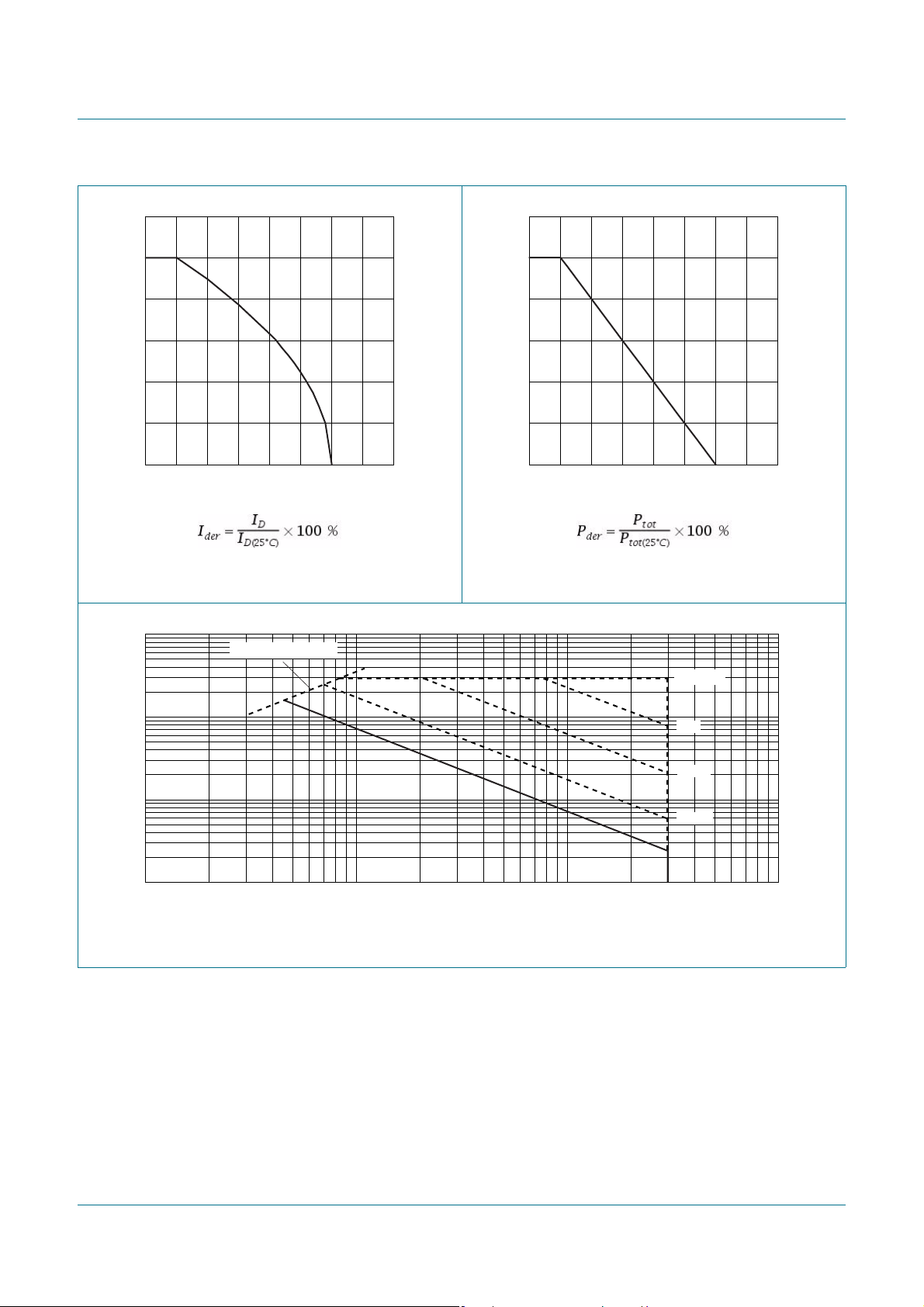
Fig 1. Normalized continuous drain current as a
function of solder point temperature
2
(A)
−10
I
D
Limit R
DSon
= VDS/I
D
120
P
der
(%)
80
40
0
0 20015050 100
003aab948
Tsp (°C)
Fig 2. Normalized total power dissipation as a
function of solder point temperature
003aab616
tp = 10 μs
−10
−10
−1
−1
−1
−10
T
= 25 °C; IDM is single pulse
sp
DC
−10−1
1 ms
10 ms
100 ms
VDS (V)
Fig 3. Safe operating area; continuous and peak drain currents as a function of drain -sou rce voltage
−10
2
PMK30EP All information provided in this document is subject to legal disclaimers. © NXP B.V. 2010. All rights reserved.
Product data sheet Rev. 04 — 25 October 2010 3 of 13
Page 4
NXP Semiconductors
003aab617
5. Thermal characteristics
PMK30EP
P-channel TrenchMOS extremely low level FET
Table 5. Thermal characteristics
Symbol Parameter Conditions Min Typ Max Unit
R
th(j-sp)
thermal resistance from junction to
see Figure 4 --18K/W
solder point
2
10
Z
th(j − sp)
(K/W)
10
δ = 0.5
0.2
0.1
0.05
1
10
10
0.02
single pulse
−1
−2
−4
10
P
t
p
−3
10
−2
10
−1
110
10 10
T
tp (s)
δ =
t
p
T
t
2
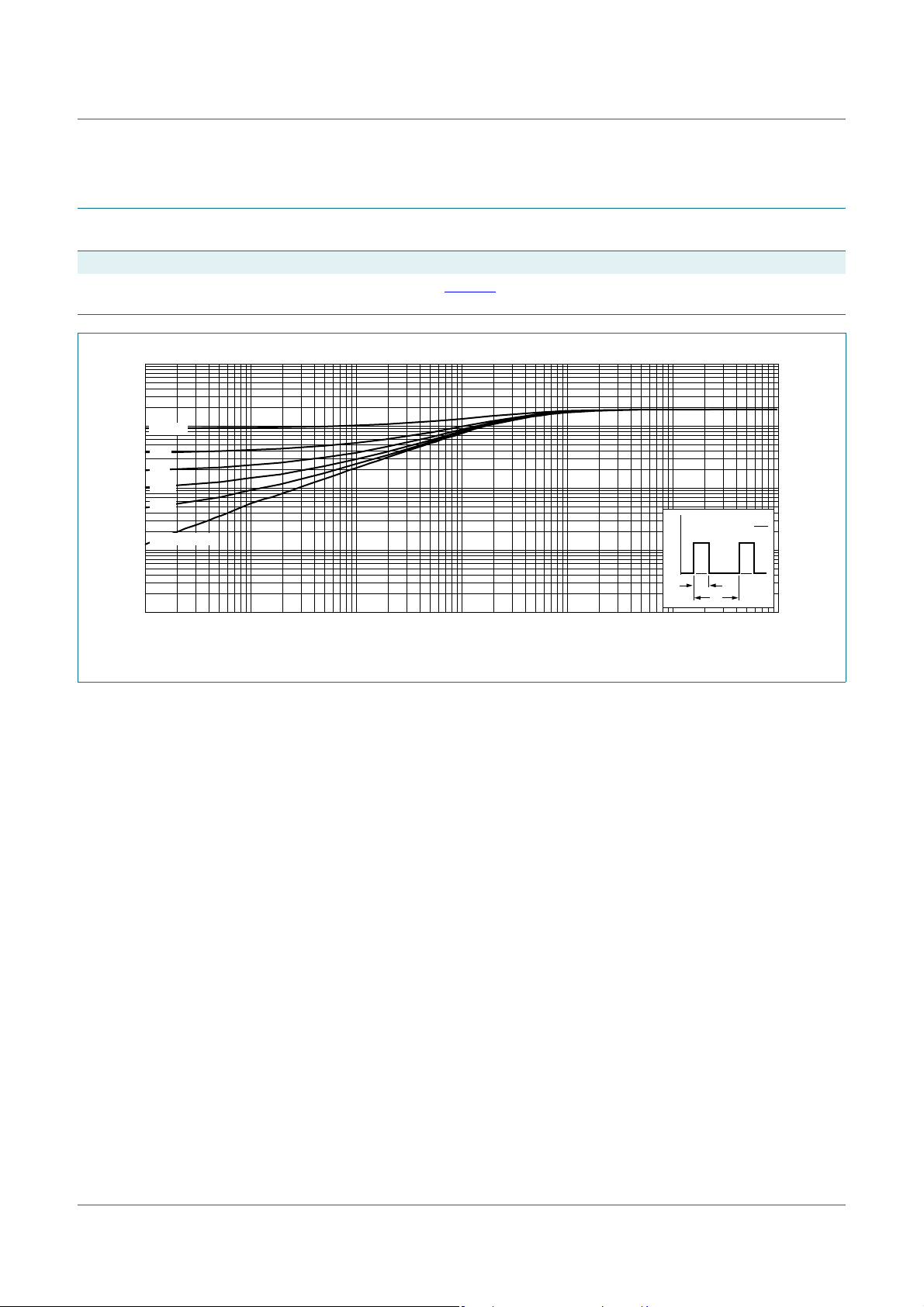
Fig 4. Transient thermal impedance from junction to solder point as a function of pulse duration
PMK30EP All information provided in this document is subject to legal disclaimers. © NXP B.V. 2010. All rights reserved.
Product data sheet Rev. 04 — 25 October 2010 4 of 13
Page 5
NXP Semiconductors
6. Characteristics
PMK30EP
P-channel TrenchMOS extremely low level FET
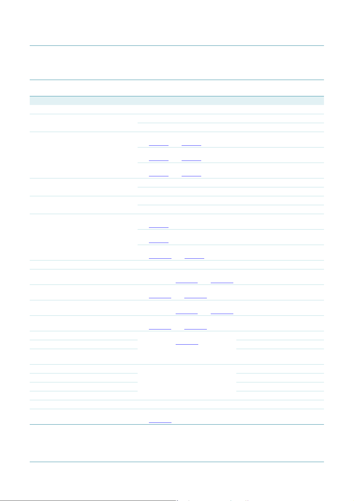
Table 6. Characteristics
Symbol Parameter Conditions Min Typ Max Unit
Static characteristics
V
(BR)DSS
V
GS(th)
drain-source breakdown
voltage
gate-source threshold
voltage
ID=-250µA; VGS=0V; Tj=25°C -30--V
=-250µA; VGS=0V; Tj=-55°C -27--V
I
D
ID=-250µA; VDS=VGS; Tj=25°C;
-1 - -3 V
see Figure 7; see Figure 8
=-250µA; VDS=VGS; Tj= 150 °C;
I
D
see Figure 7
I
=-250µA; VDS=VGS; Tj=-55°C;
D
; see Figure 8
-0.7--V
---3.3V
see Figure 7; see Figure 8
I
DSS
I
GSS
R
DSon
drain leakage current VDS=-30V; VGS=0V; Tj=25°C ---1µA
=-30V; VGS=0V; Tj= 70 °C - - -10 µA
V
DS
gate leakage current VGS=16V; VDS=0V; Tj= 25 °C - - -100 nA
=-16V; VDS=0V; Tj= 25 °C - - -100 nA
V
GS
drain-source on-state
resistance
VGS=-10V; ID=-9.2A; Tj=25°C;
see Figure 9
=-10V; ID=-9.2A; Tj=150°C;
V
GS
- 1619mΩ
- 2531mΩ
see Figure 9
V
=-4.5V; ID=-7.3A; Tj=25°C;
GS
- 2430mΩ
see Figure 10; see Figure 9
Dynamic characteristi cs
Q
Q
Q
G(tot)
GS
GD
total gate charge ID=-9.2A; VDS=-15V; VGS=-10V;
=25°C; see Figure 11; see Figure 12
T
j
gate-source charge ID=-9.2A; VDS=-15V; VGS=-10V;
see Figure 11
; see Figure 12
gate-drain charge ID=-9.2A; VDS=-15V; VGS=-10V;
-50-nC
-7-nC
-7-nC
Tj=25°C; see Figure 11; see Figure 12
V
C
C
C
GS(pl)
iss
oss
rss
gate-source plateau
voltage
input capacitance VDS=-25V; VGS= 0 V; f = 1 MHz;
output capacitance - 325 - pF
reverse transfer
ID=-9.2A; VDS=-15V; Tj=25°C;
see Figure 11
=25°C; see Figure 13
T
j
; see Figure 12
--2.5-V
- 2240 - pF
- 220 - pF
capacitance
t
d(on)
t
r
t
d(off)
t
f
turn-on delay time VDS=-15V; RL=6Ω; VGS=-10V;
R
=6Ω; Tj=25°C
rise time - 8 - ns
G(ext)
turn-off delay time - 56 - ns
fall time - 21 - ns
-10-ns
Source-drain diode
V
SD
source-drain voltage IS= -3.45 A; VGS=0V; Tj=25°C;
- -0.8 -1.2 V
see Figure 14
PMK30EP All information provided in this document is subject to legal disclaimers. © NXP B.V. 2010. All rights reserved.
Product data sheet Rev. 04 — 25 October 2010 5 of 13
Page 6
NXP Semiconductors
PMK30EP
P-channel TrenchMOS extremely low level FET
−30
I
D
(A)
−20
−10
0
0 −0.8−0.6−0.2 −0.4
VGS (V) = −7
003aab619
−5 −4.5
−4
−3.5
−3
−2.8
VDS (V)
Tj = 25 °C VDS > ID x R
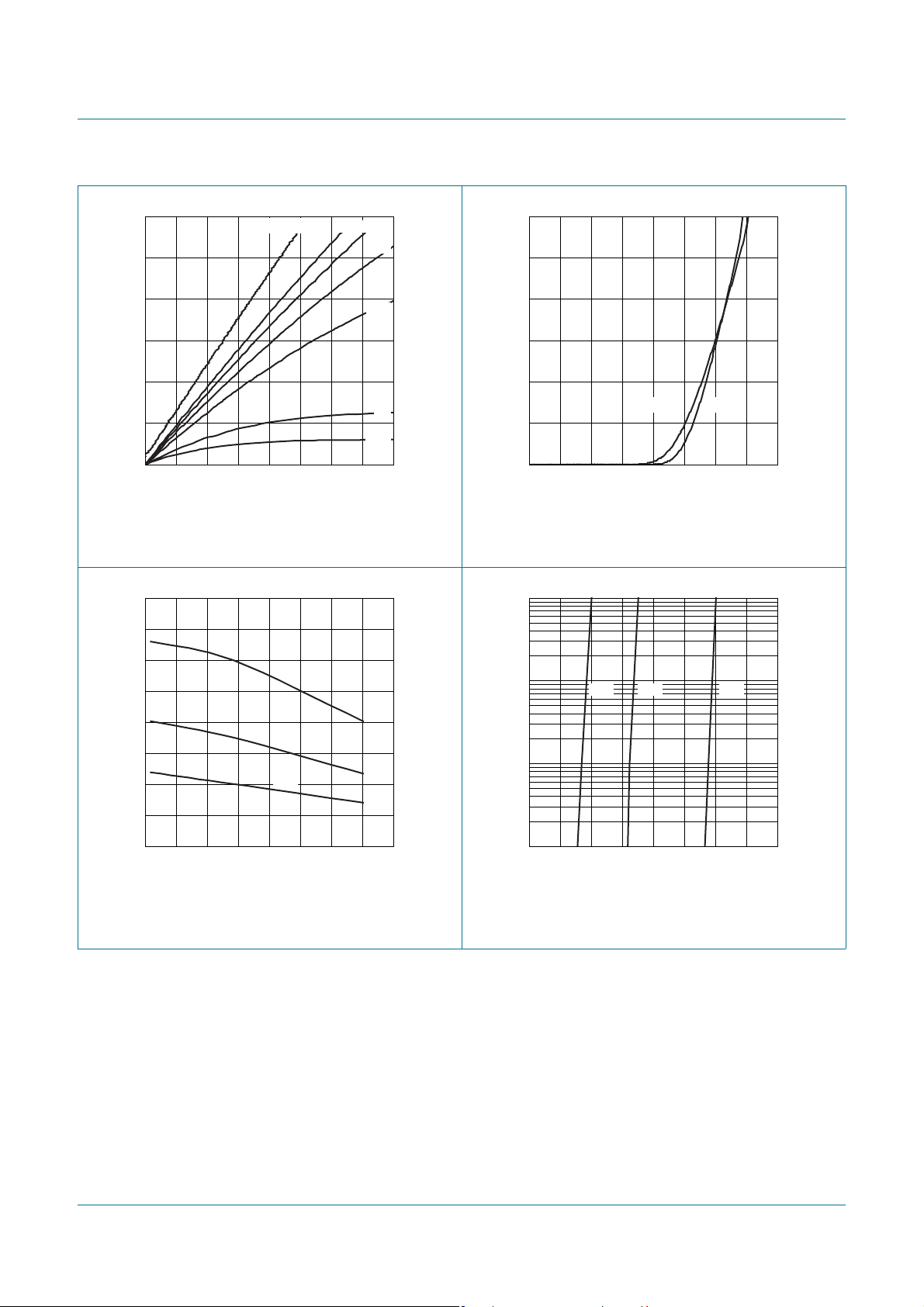
Fig 5. Output characteristics: drain current as a
function of drain-source voltage; typical values
003aab626
V
GS(th)
(V)
4
3
max
−30
I
D
(A)
−20
−10
0
0 −4−3−1 −2
Tj = 150 °C 25 °C
DSon
003aab621
VGS (V)
Fig 6. Transfer characteristics: drain current as a
function of gate-source voltage; typical value s
−10
(A)
−10
−3
I
D
−4
min typ max
003aab625
2
typ
1
0
−60 180120060
= -1 mA; VDS = V
I
D
min
Tj (°C)
GS
Fig 7. Gate-source threshold voltage as a function of
junction temperature
−5
−10
−6
−10
0 −4−3−1 −2
VGS (V)
Tj = 25 °C; VDS = -5 V
Fig 8. Sub-threshold drain current as a function of
gate-source voltage
PMK30EP All information provided in this document is subject to legal disclaimers. © NXP B.V. 2010. All rights reserved.
Product data sheet Rev. 04 — 25 October 2010 6 of 13
Page 7
NXP Semiconductors
003aaa508
PMK30EP
P-channel TrenchMOS extremely low level FET
2
a
1.6
1.2
0.8
0.4
0
−60 180120060
003aab627
Tj (°C)
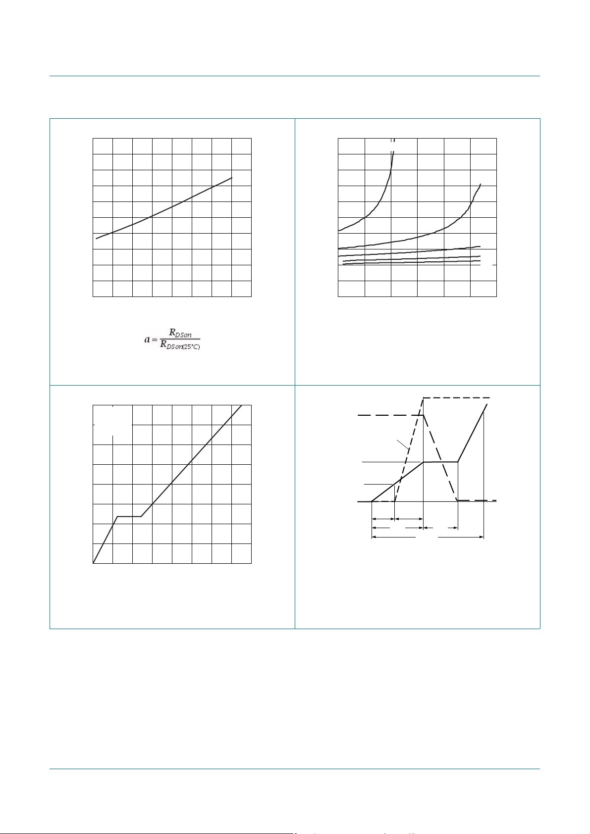
Fig 9. Normalized drain-source on-state resistance
factor as a function of junction temperature
003aab624
V
(V)
−10
GS
−7.5
VDS = −15 V
= −9.2 A
I
D
= 25 °C
T
j
100
R
DSon
(mΩ)
80
60
40
20
0
0 −30−20−10
VGS (V ) = −3
003aab620
−3.5
ID (A)
−4
−4.5
−5
Tj = 25 °C
Fig 10. Drain-source on-state resistance as a function
of drain current; typical values
V
DS
I
D
V
GS(pl)
V
−5
−2.5
0
05037.512.5 25
V
= -15 V; ID = -9.2 A; Tj = 25 °C
DS
QG (nC0
Fig 11. Gate-source voltage as a function of gate
Fig 12. Gate charge wa veform definitions
GS(th)
V
GS
Q
GS1QGS2
Q
GS
Q
G(tot)
Q
GD
charge; typical values
PMK30EP All information provided in this document is subject to legal disclaimers. © NXP B.V. 2010. All rights reserved.
Product data sheet Rev. 04 — 25 October 2010 7 of 13
Page 8
NXP Semiconductors
PMK30EP
P-channel TrenchMOS extremely low level FET
003aab623
C
iss
C
oss
C
rss
2
−10−1
VDS (V)
−10
C
(pF)
4
10
3
10
2
10
−1
−10
VGS = 0 V; f = 1 MHz VGS = 0 V
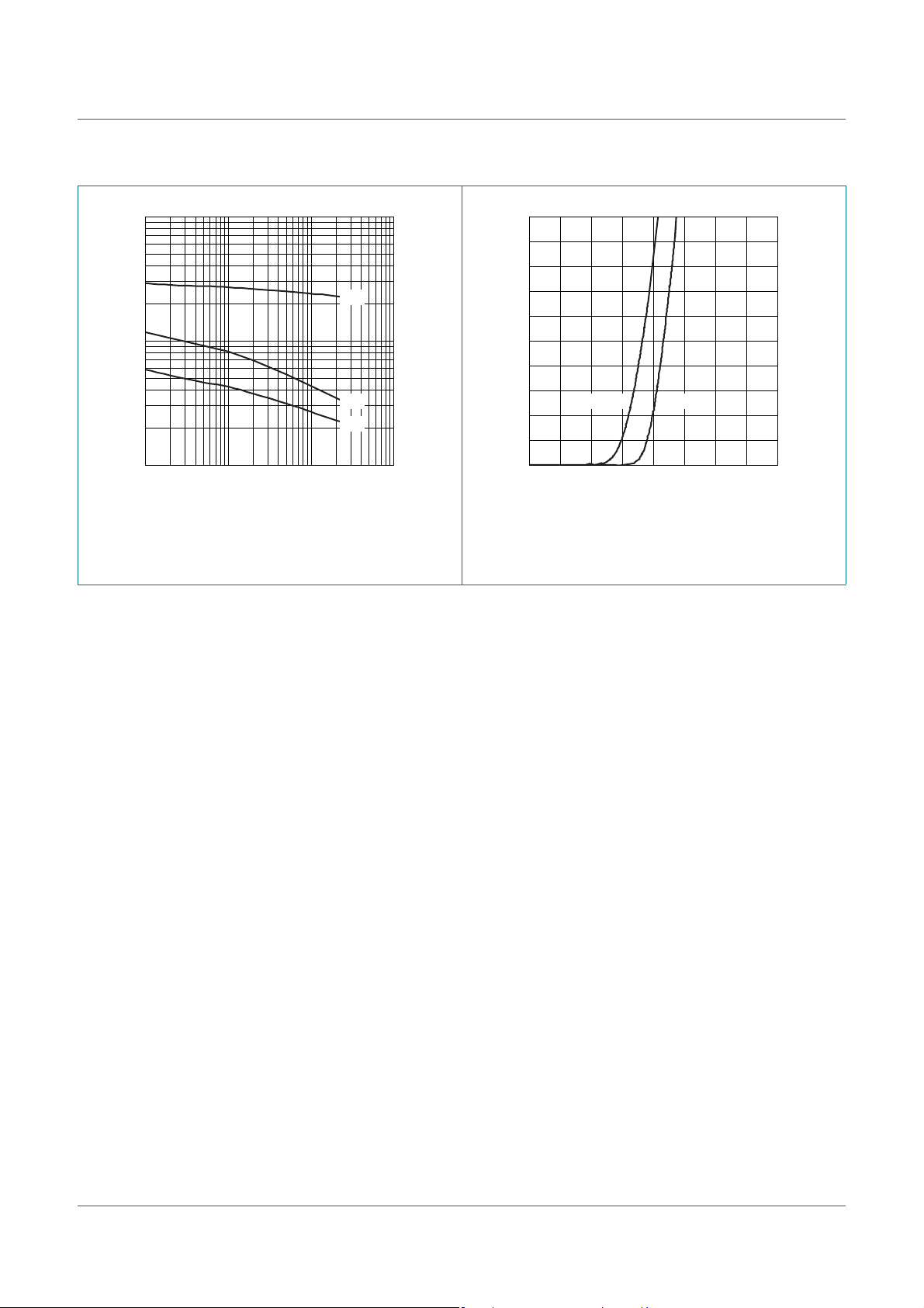
Fig 13. In put, output and reverse trans fer capacitances
as a function of drain-source voltage; typical
values
−25
I
S
(A)
−20
−15
−10
−5
0
Tj = 150 °C 25 °C
0 −1.6−1.2−0.4 −0.8
003aab622
VSD (V)
Fig 14. Sourc e current as a function of source-drain
voltage; typical values
PMK30EP All information provided in this document is subject to legal disclaimers. © NXP B.V. 2010. All rights reserved.
Product data sheet Rev. 04 — 25 October 2010 8 of 13
Page 9
NXP Semiconductors
S
-1
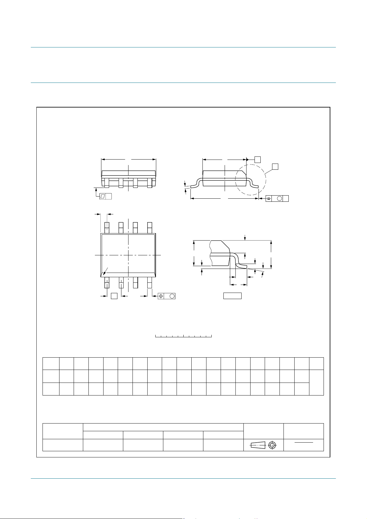
7. Package outline
PMK30EP
P-channel TrenchMOS extremely low level FET
O8: plastic small outline package; 8 leads; body width 3.9 mm
y
Z
8
pin 1 index
1
D
c
5
A
2
A
1
4
e
w M
b
p
E
H
E
detail X
A
Q
(A )
L
p
L
A
3
θ
X
v M
A
SOT96
0 2.5 5 mm
scale
DIMENSIONS (inch dimensions are derived from the original mm dimensions)
mm
OUTLINE
VERSION
SOT96-1
A
A1A2A3b
max.
0.25
1.75
0.10
0.010
0.069
0.004
p
1.45
1.25
0.057
0.049
IEC JEDEC JEITA
076E03 MS-012
0.25
0.01
0.49
0.36
0.019
0.014
0.25
0.19
0.0100
0.0075
UNIT
inches
Notes
1. Plastic or metal protrusions of 0.15 mm (0.006 inch) maximum per side are not included.
2. Plastic or metal protrusions of 0.25 mm (0.01 inch) maximum per side are not included.
(1)E(2)
cD
5.0
4.8
0.20
0.19
REFERENCES
eHELLpQZywv θ
4.0
3.8
0.16
0.15
1.27
0.05
6.2
5.8
0.244
0.228
1.05
1.0
0.4
0.039
0.016
0.7
0.6
0.028
0.024
0.25 0.10.25
0.010.010.041 0.004
EUROPEAN
PROJECTION
(1)
0.7
0.3
0.028
0.012
ISSUE DATE
99-12-27
03-02-18
o
8
o
0
Fig 15. Package outline SOT96-1 (SO8)
PMK30EP All information provided in this document is subject to legal disclaimers. © NXP B.V. 2010. All rights reserved.
Product data sheet Rev. 04 — 25 October 2010 9 of 13
Page 10

NXP Semiconductors
8. Revision history
PMK30EP
P-channel TrenchMOS extremely low level FET
Table 7. Revision history
Document ID Release date Data sheet status Change notice Supersedes
PMK30EP v.4 20101025 Product data sheet - PMK30EP v.3
Modifications:
PMK30EP v.3 20100429 Product data sheet - -
• Various changes to content.
PMK30EP All information provided in this document is subject to legal disclaimers. © NXP B.V. 2010. All rights reserved.
Product data sheet Rev. 04 — 25 October 2010 10 of 13
Page 11

NXP Semiconductors
PMK30EP
P-channel TrenchMOS extremely low level FET
9. Legal information
9.1 Data sheet status
Document status
Objective [short] data sheet Development This document contains data from the objective specification for product development.
Preliminary [short] data sheet Qualification This document contains data from the preliminary specification.
Product [short] data sheet Production This document contains the product specification.
[1] Please consult the most recently issued document before initiating or completing a design.
[2] The term 'short data sheet' is explained in section "Definitions".
[3] The product status of device(s) described in this document may have changed since this document was published and may differ in case of multiple devices. The latest product
status information is available on the Internet at URL http://www.nxp.com.
[1][2]
Product status
[3]
Definition
9.2 Definitions
Draft — The document is a draft version only. The content is still under
internal review and subject to formal approval, which may result in
modifications or additions. NXP Semiconductors does not give any
representations or warranties as to the accuracy or completeness of
information included herein and shall have no liability for the consequences of
use of such information.
Short data sheet — A short data sheet is an extract from a full data sheet
with the same product type number(s) and title. A short data sheet is intended
for quick reference only and should not be relied u pon to co nt ain det ailed and
full information. For detailed and full information see the relevant full data
sheet, which is available on request via the local NXP Semiconductors sales
office. In case of any inconsistency or conflict with the short data sheet, the
full data sheet shall prevail.
Product specification — The information and data provided in a Product
data sheet shall define the specification of the product as agreed between
NXP Semiconductors and its customer, unless NXP Semiconductors and
customer have explicitly agreed otherwise in writing. In no event however,
shall an agreement be valid in which the NXP Semiconductors product is
deemed to offer functions and qualities beyond those described in the
Product data sheet.
9.3 Disclaimers
Limited warranty and liability — Information in this document is believed to
be accurate and reliable. However, NXP Semiconductors does not give any
representations or warranties, expressed or implied, as to the accuracy or
completeness of such information and shall have no liability for the
consequences of use of such information.
In no event shall NXP Semiconductors be lia ble for any indirect, incidental,
punitive, special or consequential damages (including - without limitation - lost
profits, lost savings, business interruption, costs related to the removal or
replacement of any products or rework charges) whether or not such
damages are based on tort (including negligence), warranty, breach of
contract or any other legal theory.
Notwithstanding any damages that customer might incur for any reason
whatsoever, NXP Semi conductors’ aggregat e and cumulative liabil ity towards
customer for the products described herein shall be limited in accordance
with the Terms and conditions of commercial sale of NXP Semiconductors.
Suitability for use — NXP Semiconductors products are not designed,
authorized or warranted to be suitable for use in life support, life-critical or
safety-critical systems or equipment, nor in applications where failure or
malfunction of an NXP Semiconductors product can reasonabl y be expected
to result in personal injury, death or severe property or environmental
damage. NXP Semiconductors accepts no liability for inclusion and/or use of
NXP Semiconductors products in such equipment or applications and
therefore such inclusion and/or use is at the customer’s own risk.
Quick reference data — The Quick reference data is an extract of the
product data given in the Limiting values and Characteri stics sections of this
document, and as such is not complete, exhaustive or legally binding.
Applications — Applications that are described herein for any of these
products are for illustrative purposes only. NXP Semiconductors makes no
representation or warranty that such applications will be suitable for the
specified use without further testing or modification.
Customers are responsible for the design and operation of their applications
and products using NXP Semiconductors products, and NXP Semiconductors
accepts no liability for any assistance with applications or customer product
design. It is customer’s sole responsibility to determine whether the NXP
Semiconductors product is suitable and fit for the customer’s applications and
products planned, as well as for the planned application and use of
customer’s third party customer(s). Customers should provide appropriate
design and operating safeguards to minimize the risks associated with their
applications and products.
NXP Semiconductors does not accept any liability related to any default ,
damage, costs or problem which is based on any weakness or default in the
customer’s applications or products, or the application or use by customer’s
third party customer(s). Customer is responsible for doing all necessary
testing for the customer’s applications and products using NXP
Semiconductors products in order to avoid a default of the applications and
the products or of the application or use by customer’s third part y
customer(s). NXP does not accept any liability in this respect.
Limiting values — Stress above one or more limiting values (as defined in
the Absolute Maximum Ratings System of IEC 60134) will cause permanent
damage to the device. Limiting values are stress ratings only and (proper)
operation of the device at these or any other conditions above those given in
the Recommended operating conditions section (if present) or the
Characteristics sections of this document is not warranted. Constant or
repeated exposure to limiting values will permanently and irreversibly affect
the quality and reliability of the device.
Right to make changes — NXP Semiconductors reserves the right to make
changes to information published in this document, including without
limitation specifications and product descriptions, at any time and without
notice. This document supersedes and replaces all information supplied prior
to the publication hereof.
PMK30EP All information provided in this document is subject to legal disclaimers. © NXP B.V. 2010. All rights reserved.
Terms and conditions of commercial sale — NXP Semiconductors
products are sold subject to the general terms and conditions of commercial
sale, as published at http://www.nxp.com/profile/terms
agreed in a valid written individual agreement. In case an individual
agreement is concluded only the terms and conditions of the respective
, unless otherwise
Product data sheet Rev. 04 — 25 October 2010 11 of 13
Page 12

NXP Semiconductors
PMK30EP
P-channel TrenchMOS extremely low level FET
agreement shall apply. NXP Semiconductors hereby expressly objects to
applying the customer’s general terms and conditions with regard to the
purchase of NXP Semiconductors products by customer.
No offer to sell or license — Nothing in this document may be interpret ed or
construed as an offer to sell products that is open f or acceptance or the grant,
conveyance or implication of any license under any copyrights, patents or
other industrial or intellectual property rights.
Export control — This document as well as the item(s) described herein may
be subject to export control regulations. Export might require a prior
authorization from national authorities.
Non-automotive qualified products — Unless this data sheet expressly
states that this specific NXP Semiconductors product is automotive qualified,
the product is not suitable for automotive use. It i s neither qua lif ied nor test ed
in accordance with automotive testing or application requirements. NXP
Semiconductors accepts no liability for inclusion and/or use of
non-automotive qualified products in automotive equ ipment or applications.
In the event that customer uses the product for design-in and use in
automotive applications to automotive specifications and standards, customer
(a) shall use the product without NXP Semiconductors’ warranty of the
product for such automotive applications, use and specifications, and (b)
whenever customer uses the product for automotive applications beyond
NXP Semiconductors’ specifications such use shall be solely at customer’s
own risk, and (c) customer fully indemnifies NXP Semiconductors for any
liability, da mages or failed produ ct cl aims resulting from custome r design and
use of the product for automotive applications beyond NXP Semiconductors’
standard warranty and NXP Semiconductors’ product specifications.
9.4 Trademarks
Notice: All referenced brands, prod uct names, service names and trad emarks
are the property of their respective owners.
Adelante, Bitport, Bitsound, CoolFlux, CoReUse, DESFire, EZ-HV,
FabKey, GreenChip, HiPerSmart, HITAG, I²C-bus logo, ICODE, I-CODE,
ITEC, Labelution, MIFARE, MIFARE Plus, MIFARE Ultralight, MoReUse,
QLPAK, Silicon Tuner, SiliconMAX, SmartXA, STARplug, TOPFET,
TrenchMOS, TriMedia and UCODE — are trademarks of NXP B.V.
HD Radio and HD Radio logo — are trademarks of iBiquity Digital
Corporation.
10. Contact information
For more information, please visit: http://www.nxp.com
For sales office addresses, please send an email to: [email protected]
PMK30EP All information provided in this document is subject to legal disclaimers. © NXP B.V. 2010. All rights reserved.
Product data sheet Rev. 04 — 25 October 2010 12 of 13
Page 13

NXP Semiconductors
11. Contents
1 Product profile. . . . . . . . . . . . . . . . . . . . . . . . . . .1
1.1 General description . . . . . . . . . . . . . . . . . . . . . .1
1.2 Features and benefits. . . . . . . . . . . . . . . . . . . . .1
1.3 Applications . . . . . . . . . . . . . . . . . . . . . . . . . . . .1
1.4 Quick reference data . . . . . . . . . . . . . . . . . . . . .1
2 Pinning information. . . . . . . . . . . . . . . . . . . . . . .2
3 Ordering information. . . . . . . . . . . . . . . . . . . . . .2
4 Limiting values. . . . . . . . . . . . . . . . . . . . . . . . . . .2
5 Thermal characteristics . . . . . . . . . . . . . . . . . . .4
6 Characteristics. . . . . . . . . . . . . . . . . . . . . . . . . . .5
7 Package outline . . . . . . . . . . . . . . . . . . . . . . . . . .9
8 Revision history. . . . . . . . . . . . . . . . . . . . . . . . .10
9 Legal information. . . . . . . . . . . . . . . . . . . . . . . .11
9.1 Data sheet status . . . . . . . . . . . . . . . . . . . . . . .11
9.2 Definitions. . . . . . . . . . . . . . . . . . . . . . . . . . . . .11
9.3 Disclaimers. . . . . . . . . . . . . . . . . . . . . . . . . . . .11
9.4 Trademarks. . . . . . . . . . . . . . . . . . . . . . . . . . . .12
10 Contact information. . . . . . . . . . . . . . . . . . . . . .12
PMK30EP
P-channel TrenchMOS extremely low level FET
Please be aware that important notices concerning this document and the product(s)
described herein, have been included in section ‘Legal information’.
© NXP B.V. 2010. All rights reserved.
For more information, please visit: http://www.nxp.com
For sales office addresses, please send an email to: [email protected]
Date of release: 25 October 2010
Document identifier: PMK30EP
 Loading...