

Page 1
查询PMEG2010EV供应商
DISCRETE SEMICONDUCTORS
DATA SH EET
M3D744
PMEG2010EV
Low V
MEGA Schottky barrier
F
diode
Product specification
Supersedes data of 2002 Jun 24
2003 Aug 20
Page 2
Philips Semiconductors Product specification
Low VF MEGA Schottky barrier diode
FEATURES
• Forward current: 1 A
• Reverse voltage: 20 V
• Very low forward voltage
• Ultra small SMD package
• Flat leads: excellent coplanarity and improved thermal
behaviour.
APPLICATIONS
• Low voltage rectification
• High efficiency DC/DC conversion
• Switch mode power supply
• Inverse polarity protection
• Low power consumption applications.
DESCRIPTION
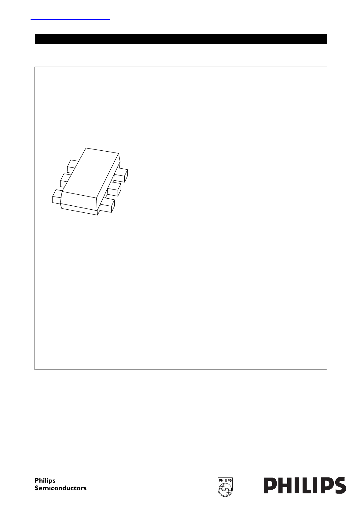
Planar Maximum Efficiency General Application (MEGA)
Schottky barrier diode with an integrated guard ring for
stress protection in a SOT666 ultra small SMD plastic
package.
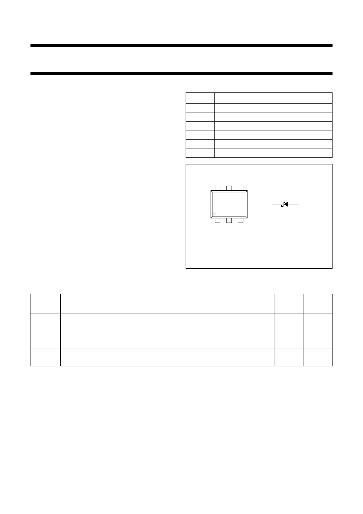
PMEG2010EV
PINNING
PIN DESCRIPTION
1 cathode
2 cathode
3 anode
4 anode
5 cathode
6 cathode
handbook, halfpage
123
Marking code: F1.
Fig.1 Simplified outline (SOT666) and symbol.
456
1, 2
5, 6
3, 4
MHC310
LIMITING VALUES
In accordance with the Absolute Maximum Rating System (IEC 60134)
SYMBOL PARAMETER CONDITIONS MIN. MAX. UNIT
V
R
I
F
I
FSM
continuous reverse voltage − 20 V
continuous forward current − 1A
non-repetitive peak forward current t = 8.3 ms half sinewave;
− 8A
JEDEC method; note 1
T
stg
T
j
T
amb
storage temperature −65 +150 °C
junction temperature − 125 °C
operating ambient temperature −65 +125 °C
Note
1. Only valid if pins 3 and 4 are connected in parallel.
2003 Aug 20 2
Page 3
Philips Semiconductors Product specification
Low VF MEGA Schottky barrier diode
PMEG2010EV
THERMAL CHARACTERISTICS
SYMBOL PARAMETER CONDITIONS VALUE UNIT
R
th j-a
thermal resistance from junction to ambient note 1 405 K/W
note 2 215 K/W
Notes
1. Refer to SOT666 standard mounting conditions.
2. Mounted on printed circuit-board, 1 cm2 copper area.
Soldering
The only recommended soldering method is reflow soldering.
ELECTRICAL CHARACTERISTICS
T
=25°C unless otherwise specified.
amb
SYMBOL PARAMETER CONDITIONS TYP. MAX. UNIT
V
F
I
R
C
d
continuous forward voltage IF= 10 mA 240 270 mV
I
= 100 mA 300 350 mV
F
I
= 1000 mA; note 1; see Fig.2 480 550 mV
F
reverse current VR= 5 V; note 2 5 10 µA
V
= 8 V; note 2 7 20 µA
R
V
= 15 V; note 2; see Fig.3 10 50 µA
R
diode capacitance VR= 5 V; f = 1 MHz; see Fig.4 19 25 pF
Notes
1. Only valid if pins 1, 2, 5 and 6 are soldered on a 1 cm
2. Pulse test: tp= 300 µs; δ = 0.02.
2
copper solder land.
2003 Aug 20 3
Page 4

Philips Semiconductors Product specification
Low VF MEGA Schottky barrier diode
GRAPHICAL DATA
VF (V)
MHC311
0.60.20 0.4
3
10
handbook, halfpage
I
F
(mA)
2
10
(1) (2) (3)
= 125°C.
=85°C.
=25°C.
(1) T
(2) T
(3) T
10
1
−1
10
amb
amb
amb
Fig.2 Forward current as a function of forward
voltage; typical values.
PMEG2010EV
20
MHC312
(1)
(2)
(3)
VR (V)
5
10
handbook, halfpage
I
R
(µA)
4
10
3
10
2
10
10
1
(1) T
(2) T
(3) T
amb
amb
amb
= 125°C.
=85°C.
=25°C.
Fig.3 Reverse current as a function of reverse
voltage; typical values.
250 51015
15
MHC313
VR (V)
80
handbook, halfpage
C
d
(pF)
60
40
20
0
05
f =1 MHz; T
amb
10 20
=25°C.
Fig.4 Diode capacitance as a function of reverse
voltage; typical values.
2003 Aug 20 4
Page 5

Philips Semiconductors Product specification
Low VF MEGA Schottky barrier diode
PMEG2010EV
PACKAGE OUTLINE
Plastic surface mounted package; 6 leads SOT666
D
S
YS
A
456
E
H
E
X
pin 1 index
123
e
DIMENSIONS (mm are the original dimensions)
UNIT b
mm
OUTLINE
VERSION
SOT666
A
0.6
0.5
0.27
0.17
cD
p
0.18
0.08
IEC JEDEC EIAJ
1
1.7
1.5
b
p
e
E
1.3
1.1
A
wM
A
0 1 2 mm
scale
e
H
L
0.3
0.1
p
w
0.1y0.1
e
1
0.5
1.0
REFERENCES
E
1.7
1.5
detail X
PROJECTION
L
p
EUROPEAN
c
ISSUE DATE
01-01-04
01-08-27
2003 Aug 20 5
Page 6

Philips Semiconductors Product specification
Low VF MEGA Schottky barrier diode
DATA SHEET STATUS
LEVEL
I Objective data Development This data sheet contains data from the objective specification for product
II Preliminary data Qualification This data sheet contains data from the preliminary specification.
III Product data Production This data sheet contains data from the product specification. Philips
Notes
1. Please consult the most recently issued data sheet before initiating or completing a design.
2. The product status of the device(s) described in this data sheet may have changed since this data sheet was
3. For datasheets describing multiple type numbers, the highest-level product status determines the data sheet status.
DATA SHEET
STATUS
published. The latest information is available on the Internet at URL http://www.semiconductors.philips.com.
(1)
PRODUCT
STATUS
(2)(3)
development. Philips Semiconductors reserves the right to change the
specification in any manner without notice.
Supplementary data will be published at a later date. Philips
Semiconductors reserves the right to change the specification without
notice, in order to improve the design and supply the best possible
product.
Semiconductors reserves the right to make changes at any time in order
to improve the design, manufacturing and supply. Relevant changes will
be communicated via a Customer Product/Process Change Notification
(CPCN).
DEFINITION
PMEG2010EV
DEFINITIONS
Short-form specification The data in a short-form
specification is extracted from a full data sheet with the
same type number and title. For detailed information see
the relevant data sheet or data handbook.
Limiting values definition Limiting values given are in
accordance with the Absolute Maximum Rating System
(IEC 60134). Stress above one or more of the limiting
values may cause permanent damage to the device.
These are stress ratings only and operation of the device
atthese or atanyother conditions above thosegivenin the
Characteristics sections of the specification is not implied.
Exposure to limiting values for extended periods may
affect device reliability.
Application information Applications that are
described herein for any of these products are for
illustrative purposes only. Philips Semiconductors make
norepresentationor warranty that suchapplicationswillbe
suitable for the specified use without further testing or
modification.
DISCLAIMERS
Life support applications These products are not
designed for use in life support appliances, devices, or
systems where malfunction of these products can
reasonably be expectedto result in personal injury.Philips
Semiconductorscustomersusing or selling theseproducts
for use in such applications do so at their own risk and
agree to fully indemnify Philips Semiconductors for any
damages resulting from such application.
Right to make changes Philips Semiconductors
reserves the right to make changes in the products including circuits, standard cells, and/or software described or contained herein in order to improve design
and/or performance. When the productis infull production
(status ‘Production’), relevant changes will be
communicated via a Customer Product/Process Change
Notification (CPCN). Philips Semiconductors assumes no
responsibility or liability for the use of any of these
products, conveys no licence or title under any patent,
copyright, or mask work right to these products, and
makes no representations or warranties that these
products are free from patent, copyright, or mask work
right infringement, unless otherwise specified.
2003 Aug 20 6
Page 7

Philips Semiconductors – a w orldwide compan y
Contact information
For additional information please visit http://www.semiconductors.philips.com. Fax: +31 40 27 24825
For sales offices addresses send e-mail to: sales.addresses@www.semiconductors.philips.com.
© Koninklijke Philips Electronics N.V. 2003
All rights are reserved. Reproduction in whole or in part is prohibited without the prior written consent of the copyright owner.
The information presented in this document does not form part of any quotation or contract, is believed to be accurate and reliable and may be changed
without notice. No liability will be accepted by the publisher for any consequence of its use. Publication thereof does not convey nor imply any license
under patent- or other industrial or intellectual property rights.
Printed in The Netherlands 613514/02/pp7 Date of release: 2003 Aug 20 Document order number: 9397 750 11684
SCA75
 Loading...