

Philips PMBTA06 Datasheet

DISCRETE SEMICONDUCTORS
DATA SH EET
ook, halfpage
M3D088
PMBTA06
NPN general purpose transistor
Product specification
Supersedes data of 1998 Jul 20
1999 Apr 29
Philips Semiconductors Product specification
NPN general purpose transistor PMBTA06
FEATURES
• High current (max. 500 mA)
• Low voltage (max. 80 V).
APPLICATIONS
• General purpose switching and amplification in e.g.
telephony and professional communication equipment.
DESCRIPTION
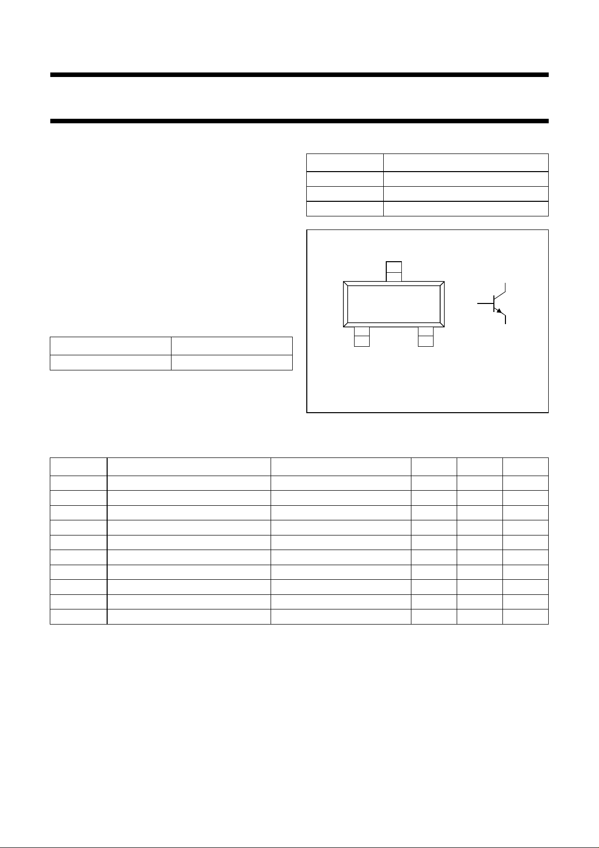
NPN transistor in a SOT23 plastic package.
PNP complement: PMBTA56.
MARKING
TYPE NUMBER MARKING CODE
(1)
PMBTA06 ∗1G
Note
1. ∗ = p : Made in Hong Kong.
∗ = t : Made in Malaysia.
PINNING
PIN DESCRIPTION
1 base
2 emitter
3 collector
handbook, halfpage
Top view
3
1
21
MAM255
Fig.1 Simplified outline (SOT23) and symbol.
3
2
LIMITING VALUES
In accordance with the Absolute Maximum Rating System (IEC 134).
SYMBOL PARAMETER CONDITIONS MIN. MAX. UNIT
V
CBO
V
CEO
V
EBO
I
C
I
CM
I
BM
P
tot
T
stg
T
j
T
amb
collector-base voltage open emitter − 80 V
collector-emitter voltage open base − 80 V
emitter-base voltage open collector − 4V
collector current (DC) − 500 mA
peak collector current − 1A
peak base current − 200 mA
total power dissipation T
≤ 25 °C; note 1 − 250 mW
amb
storage temperature −65 +150 °C
junction temperature − 150 °C
operating ambient temperature −65 +150 °C
Note
1. Transistor mounted on an FR4 printed-circuit board.
1999 Apr 29 2
Philips Semiconductors Product specification
NPN general purpose transistor PMBTA06
THERMAL CHARACTERISTICS
SYMBOL PARAMETER CONDITIONS VALUE UNIT
R
th j-a
Note
1. Transistor mounted on an FR4 printed-circuit board.
CHARACTERISTICS
=25°C unless otherwise specified.
T
amb
SYMBOL PARAMETER CONDITIONS MIN. MAX. UNIT
I
CBO
I
EBO
h
FE
V
CEsat
V
BE
f
T
thermal resistance from junction to ambient note 1 500 K/W
collector cut-off current IE= 0; VCB=80V − 50 nA
emitter cut-off current IC= 0; VEB=5V − 50 nA
DC current gain IC= 10 mA; VCE= 1 V 100 −
= 100 mA; VCE= 1 V 100 −
I
C
collector-emitter saturation voltage IC= 100 mA; IB=10mA − 0.25 V
base-emitter voltage IC= 100 mA; VCE=1V − 1.2 V
transition frequency IC= 10 mA; VCE= 2 V; f = 100 MHz 100 − MHz
1999 Apr 29 3
 Loading...