Philips PM6652, PM6654 Service Manual

Programmable
Timer
—
Counters
PM
Service
9499
465
00511
850415
First
6652,
Manual
edition
-54
Scientific
&
Scientific & Industrial
Equipment
Division
PHILIPS
CEX-board
CEX-board
Channel
TEEE-488
C,
bus
PM
PM
9610
9696
..ccccceseccccessecscenee
..
10-18
10-20
(PM
(PM
6654),
6652),
U6
U7
wccceseccceeescceeve
10-16
10-14
Display-board,
Rear
panel
board,
US
....eeececcceccseeeeses
10-12
Keyboard
Input
Amplifier
Unit,
U4
U3
and
.rescccccseccncccsccscesee
..csseeeeccccencceccceesee
10-10
10-8
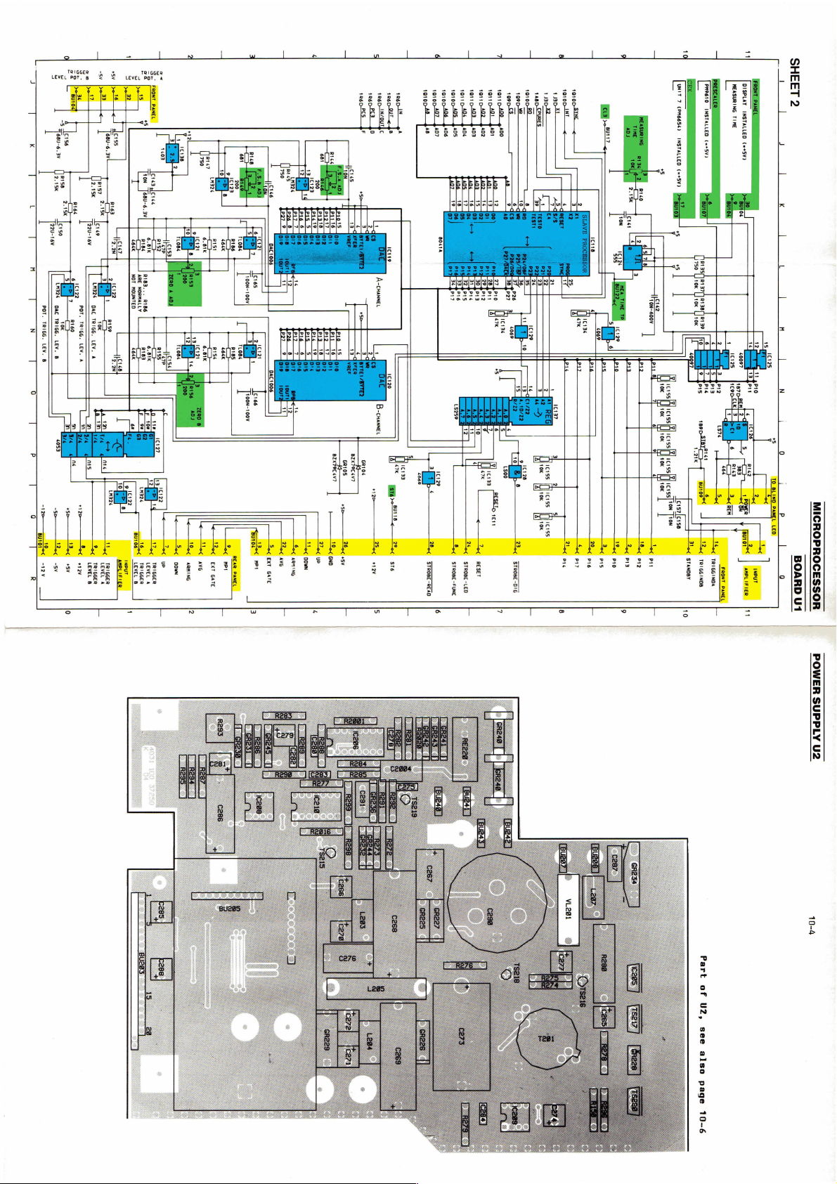
Power
Supply
board,
U2
.
10-4
How
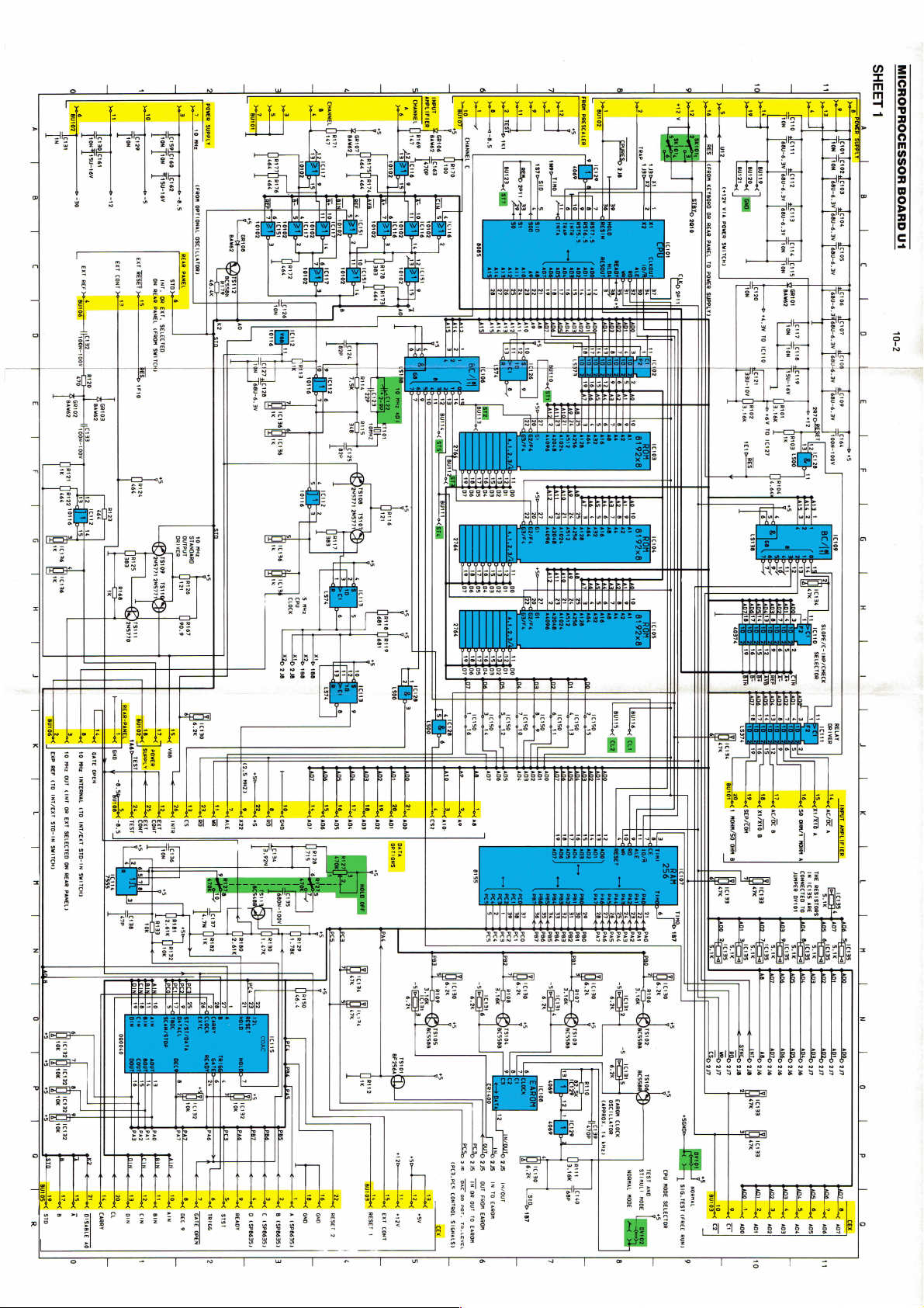
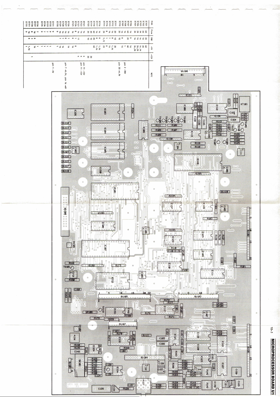
Microprocessor
board,
U1
eceseeeecccereseeee
10-2
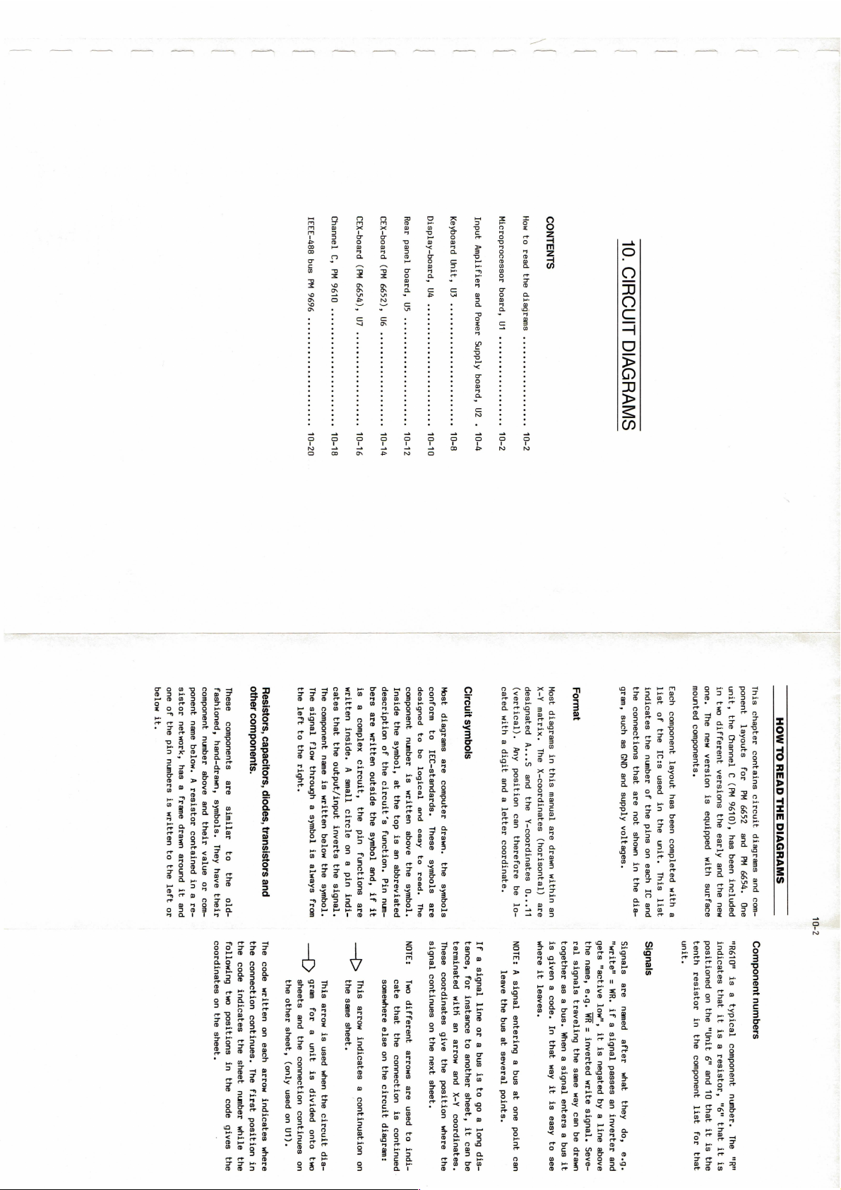
CONTENTS
to
read
the
diagrams
...ceceeseeeeeeeeee
10-2
10.
CIRCUIT
DIAGRAMS
one
below
of
it.
the
pin
numbers
is
written
to
the
left
or
component
ponent
sistor
name
network,
number
below.
has
above
A
a
resistor
frame
and
their
drawn
contained
value
around
in
or
it
a
com-
re-
and
other
These
fashioned,
components.
components
hand-drawn,
are
symbols.
similar
They
to
have
the
their
old-
the
the
coordinates
following
connection
code
indicates
two
on
positions
the
continues.
sheet.
the
sheet
in
The
the
first
number
code
position
gives
while
the
the
in
the
Resistors,
capacitors, diodes,
The
left
signal
to
flow
the
right.
through
a
symbol
transistors
is
always
and
from
The
sheets
the
other
and the
sheet,
connection
(only
used
continues
on
U1).
on
{>
gram
for
a
unit
is
divided
onto
two
code
written
on
each
arrow
indicates
where
cates
written
The
component
that
inside.
the
name
output/input
A
small
is
written
circle
inverts
below
on
a
the
the
pin
signal.
symbol.
indi-
the
This
same
arrow
sheet.
is
used
when
the
circuit
dia-
bers
description
is
Inside
a
are
complex
the
written
symbol,
of
circuit,
the
outside
at
circuit’s
the
the
the
top
pin
function.
symbol
is
an
functions
abbreviated
and,
Pin
if
num-
are
it
>
somewhere
cate
This
that
arrow
else
the
indicates
on
connection
the
circuit
a
continuation
is
diagram:
continued
on
conform
designed
component
to
to
number
be
IEC-standards.
logical
is
written
and
These
easy
above
to
symbols
the
read.
symbol.
are
The
signal
NOTE:
continues
Two
different
on
the
arrows
next
sheet.
are
used
to
indi-
Circuit
Most
diagrams
symbols
are
computer
drawn.
the
symbols
tance,
terminated
If
These
a
signal
coordinates
for
instance
with
line
an
or
give
to
arrow
a
bus
another
the
and
is
position
to
sheet,
X-Y
go
coordinates.
a
where
it
long
can
dis-
the
be
designated
X-Y
cated
(vertical).
matrix.
with
a
A...S
Any
The
digit
position
X-coordinates
and
and
the
a
letter
can
Y-coordinates
therefore
(horisontal)
coordinate.
be
0...11
are
lo-
where
NOTE:
A
it
leave
signal
leaves.
the
entering
bus
at
several
a
bus
points.
at
one
point
can
Most
Format
diagrams
in
this
manual
are
drawn
within
an
together
is
ral
given
signals
as
a
code.
a
traveling
bus.
In
When
that
the
a
way
signal
same
it
way
enters
is
can
easy
be
a
to
bus
drawn
see
it
gets
the
"write"
name,
"active
=
e.g.
WR.
low",
if
WR
a
=
signal
it
inverted
is
negated
passes
write
by
an
signal.
a
inverter
line
Seve-
above
and
gram,
the
indicates
connections
such
the
as
GND
number
that
and
of
are
supply
the
not
pins
voltages.
shown
on
in
each
the
IC
dia-
and
Signals
Signals
are
named
after
what
they
do,
e.g.
Each
list
component
of
the
IC:s
layout
used
has
in
been
the
completed
unit.
This list
with
a
mounted
one.
The
components.
new
version
is
equipped
with
surface
positioned
tenth
unit.
resistor
on
the
in
"Unit
the
component
6"
and
10
that
list
it
for
is
that
the
unit,
ponent
in
two
the
different
layouts
Channel
for
versions
C
(PM
PM
9610),
6652
the
and
early
has
been
PM
and
6654.
included
the
new
One
"R610"
indicates
is
that
a
typical
it
is
component
a
resistor,
number.
"6"
that
The "R"
it is
This
chapter
HOW
TO
contains
READ
circuit
THE
DIAGRAMS
diagrams
and
com-
Component
numbers
10-2
+
|
A
]
8
T
Hoon-t00v
c132
R120
oe
EXT
CONT
c
Ly)
T
E
T
R121
«
F
T
G
T
H
T
T
K
EXP
REF
]
(TO
INT/EXT
U
STD-IN
SWITCH)
T
u
T
N
T
0
5
10K
I
+5
10K
P
+5
10k
+5
I
10k
3
1
sTD
R
10
10
MHz
MHz
OUT
INTERNAL
(INT
OR
(TO
EXT
INT/EXT
SELECTED
STD-IN
ON
REAR
SWITCH)
PANEL)
1¢132(P]]
;
1¢132[)]
’
1c132(P]]
1c132
3
2N5770
GATE
OPEN
cL
CARRY
Din
DISABLE
AO
_
1
ext
—
RESET
ANEL
xT.
SELECTED
(FROM
SWITCH)
1F10
+5
rae
DRIVER
ouTpuT
Ts
ee
.
AIN
CIN
BIN
vec
9
om:
i
STANDARD
GATE
OPEN
+
4
2
Sin
=
3
RIT7E]RIT6
466
11466
AO
10N
]68U-6.3V
4
|
Ui
ps1
10
MHz
(2,5
+s)
MHZ)
|
Qj
toi
6
TRIGG
stst
2
READY
=
D
C
(SP8635)
(P8635)
8
¢spes3s)
|
|3
46.4
R150
A
GNO
(SP8635)
7
47k
5
Y
5
|
47k
reser
Gono
2
|
14
10136
113%
‘«
=
3
oe
681
RIB
P]RIN9
Leet
R112
+12
+5)
RESET:
ext
+12v
cont
if
|
|
/
|_
5
4
264
ta
Fr
19907
2764
4
4
BU123,
st?
a
26
a
i
B
eT
i
13
1302
12}o1
11
6
0S
$03
400
Ds
7
ano
1s7>S!2__$
4069
>
Lino
211
AS
3
wt
Ang
03
a3
ra
B
5
;
re
sot
22
A
26
A
4
{ths
1c120
[se
3
AD
02
ani}
ADS
te
Ag
as
4
25
$,
848
413
1c150
C159,
1c129
3.16K
“Tésp
7
1c150
Ring
[C140
245
1c150
pAD2
‘ADt
ADO
(APPROX.
4p5232.
TZ
70P
16
kH2)
|
3p
t-———L550
215
2s
(PC3.PCS
—_
DAC
“IW
or
CONTROL
OR
our
POT.
To
SIGNALS)
TR.
EAROM
LEVEL
=
iA
rT
+14
|
D6
ADS
Janz
7
PCS
—_eaicog
248
IN
D235
24S
QUT
IN
IN/OUT
TO
FROM
EAR}
EAROM
"
6
10
—_
1150
6.2K
LSID,
yay
1130
|
al
387
35
31
ADI
AD3
ap2
|
=
[7
6
AI
AL
u
AZ
AZ
AL
4
LBS
LBUt16,¢
iz
oc
(eal
cla
EAROM
OSCILLATOR
CLOCK
NORMAL
MODE
8
32
ADO.
30
U
1
STIMUL!
MODE
=
36
37
ts
ty
pcto2
1103
1106
1105
TEST
AND
+S
[—
9
1c101
ChKS
2011
TC107
10
CPU
MODE
SIG.TEST
3
SELECTOR
(FREE
RUN)
,
4
(FROM
KEYBORD
(412V
VIA
OR
POWER
REAR
PANEL
SWITCH)
TO
POWER
SUPPLY)
1
+
40376
1
MOHH/SO
OHH
~~
|
s
47K
10133
+s
NORMAL
ma
tr
@
n
10
68U-6.
3V
]68U-6.3V
GND
]68U-6.3V
]10N
]10N
c120
=
10N
+46.3V
TO
1C110
R102
3.16k
1E1D————4
m=
6
5
‘
Lst38
7
9
1
7,
te]
18
Te
a
7
19
6
5
2
7
his
icia3
pAna_2fya]
paD2
_7F—Sq]
itias
5.1K
S.1k
|
p48
GAD
_A8
22
—______ADE,
eT
AD7,
246
26
og
9
4g
47k
1133
ep
47k
10
7
Legh
Sa
eh?
Slag
Fewer
Jion
fers7
T
ion
Jere
‘Tisu-16v
cis
+5
FI
2
1
11
iF
rE
14
1
47k
10136
At
rn
3
o
ic119
SELECTOR
CONNECTED
THE
JUMPER
IN
1135
RESISTORS
DV101
ARE
TO
$ADS
6F—F—)
icras
1c135
3.1K
5.1K
Japs
P23$
$AD4
485
CADE
ADI
216
yy
yg
7
4
Hid
4
cro
it
4
[c1024]c103
I
pmiekd
B
intone
C106
|
ycr0s.
banca
ia
"Tésu-6.3468U-6.3V
aicios
|
ycio7
D
sy
[68U-6.3V
c108
[68U-6.3V
4[C109
E
]100N-100V
[e164
5
E
L
HEsOs)
G
l
2|
H
SLOPE/C-1NP/CHECK
|
|
J
|
K
|
L
cee
Ic135
5.1K
ae
$aps
fds
Od
664)
Seq]
rias
1135
M
qant_________ADt
$a02
pADO
ADR,
—_A0,,
|
N
|
9
9
247
47
7
0
P
L
Qo
Hit
MICROPROCESSOR
BOARD
U1
10-2
SASRS
eegedg
SYeek
wean
ao
ara
ou
ro
,
a
SAS5S5
geddd
S8Sa8
YEESS
©
©
~
2s
aan
=
2 z
E
5
=
&
s
eer
SS555
SREBNR
Meee s wOaae
e252 2 20
SSSSS S5555
SShRR
SBSRR
BERS
&
wwe
oo
BR
Fe
EB.
5
~
&
2
&
Z
E
Be
5
ES
2
wee
FR
Pe
RP
EE
35
ae
a=
wt
ah
es)
22
BSSBSES
Seatcuan
SSSRX
ea
snoo
ses
Bos
or
NN
ss
ee
ar
ae
ee
SESES
S2SBS5
FGEGRS
VOoeNy
ST
wore
on
Fs
NOte=N
S78
ee
SHSASS
25865
SBEGR
Noo
SRS
Bs
a
es
SRRER
se
pe
3S
ss
ps
a7"
Sa
2
EB
B
55
yoOoN
8
uw
t 8
2
u
2 3
SBESSSI]
Seass|
FESRES
pone | =
BESTS!
gezgep]e
BReESS|
RRRSE]
LEE
RRB
88
SF
3
2
3
2
+
&
z
+
4
cs}
2
é
7
J}
3
Se
..
-
Hi
ee
ee
noe
£-OL
HOSSAD0HdOHDIN
GuVvOd
+N
q
L
Pa
3.
&
as
y
&
J
6
s
(M324
ieigg
T
7
POT:
DAC
POT.
TRIGG.
R160
TRIGG.
10K
TRIGG.
N
LEV.
LEV,
LEV.
B
B
T
A
0
1
ce
+5v
~
s
¥
M324
10122
1
DAC
JAC
TRIGG.
RI59
a
TRIGG.
LE
Vea
NOT
MOUNTED
64k
ze
as
3.
a
R1B3,,.
ARE
NORMALLY
R186
oe
as
—_(_}—+
+t}
TLOBS
6.81K
R186
464K
RIS!
Ic
Tort
DAC
2
1006
Teves
T
100N-100¥
1247
1419
2
18
16
12
7
1011
1010
1010)
101
1010)
1R6p-h__pA
1R6-OUl
1RED-NCOUTEC
<
48
L-
7
15
16
icit9
A-CHANNEL
[
BZX79C4V7
B2X79C4V7
GR10S
ns
41—
Ht
00-A07_4.407
ade
Ans
An
ae
BOSTA
ETS
(I
4
ns
1011
A03
EID
Covi
1011
AD2
29
307
Yoi2
P13
1011
apt
28,
p11
fore
ane,
27
}e10
+5
1010082
sag
noe
1091
pSPuges
TPURES.
we
7
ET]
to
4
8
6
9
23
2
35
36
37
38]
p26
p27
10k
10k
ii
131
7
27
2
10155,
C155,
10101
1010p-1NT
2
3
4
5
a
1
Piz
14
P14
=
Bu1I7
2
}
15
10N
RISK
Tete
pia
R140
12
|
+s
Ty
jf
142
on-a00v
11.8
10K
1c1s5,
i
10K
icissi
§
10K
Ic1ss)
5
10K
icrssi
4
10K
Ic1ss|
UNIT
7
(PM6654)
INSTALLED
(=+5¥)
+5
=
750
10K
10K
10K
DISPLAY
PHO61O
MEASURING
INSTALLED
INSTALLED
TIME
(=S¥)
(=+SV)
R135/]R1377]
R138)
]
R139.
r
\ |
J
|
K
|
L
|
M
_|
MICROPROCESSOR
:
AVG
{aieere
o12v
a
0
|
|
TRIGGER
‘
poh
TRIGGER
-—
up
TRIGGER
LEVEL_8
aoe
now
ARMING
2
EXT
T
GATE
_
}-
3
4
‘sre
+12V
i
|
|
|
aa
5
}
|
STROBE
STROBE
STROBE-READ
-LED
-FUNC
|
6
RESET
7
oe
STROBE-D'G
Pts
i
z=
8
9
p13
pia
PIO
ps
P16
ia
Pit
i
STANDBY
TRIG61NDB
10
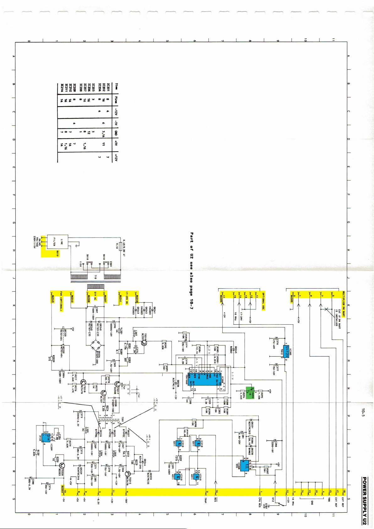
Part
TRIGGINOA
_
o
n
|
POWER
SUPPLY
U2
10-4
of
U2,
see
also
page
10-6
_|
(0)
=]
1
_|
q
el
J
_
4
SI
|
7
J
>
7
4
a
|
9|
10|
WW
1209
Icz0
1c211
B
T
C
T T
1214
8
4
16
14
4
7
7
8
7
14
14
1,16
E
T
T
A
230V/115V
VOLTAGE
MAINS
T
az
K
T
T
A
T
N
P
T
q
T
R
T
25
FILTER
LINE
—
ZY
RE220
HE321A04
ea
RE220
—YHES21A04
oe
2020
T220N-100¥
-
£2006
+sv
il
cana
BZW70CSV6
ics
1c207
1c208
|
|
46
16
6
8
12
1
1,16
aei8
415¥
|
oul
%ezt03-c33
T
deen
T
GR229
1c208
tcmz
1¢201
1c275
|
|]
|
8
8
3
16
4
4
6
|
3,14]
3
44
7
7
sx10
Ir
110
eae7
100N-100V
sp
|
anzee
82T03-C33
in
260
be
ervesc
—
i
[eves
1
1000U-10¥
a
aaa
ee
Itea
Pine
|
-12V
|
-5V
|
GND
|
+5V
+12V
0.40/0.80
eS
vu
aT
1N4003
1N4003
1NS003
GR262
GR243
Dt
4
|
c290
7
ney
‘GR225
BYVOSC
+
Teeos
1
Te270
:
“20
rr
BYv9sc
yw
Tarn
GR261
Dt
R2631C279
10k
T33u-10v
|
[2.2N
|c278
TOA
BZX79C16
O60
GR236
ft
“Tow
av
Part
of
U2
see
also
page
10-7
4.2V
R286
12.tk]
4.5
[4.
Vv
Ts
LY
mE!
{0
3
15
16
|c2ao
R285
sox
[)R2001
Li6.exK|
16
i
3 4
1206"
-4
A
=e
R245
BAws2
sem
_|
[ys2ee
|
|
R289
fea
|
|
|
pyoR231
®azxzocava
lees
R286
L)26.1K'Y
1
GR230
aawe2
B
|
c
|
E
|
|
H
J
Li
+SV
|
__t
C276
aaa
1c205
7812
2
aia
C277
i
:
j
|
|
|
boas
pe
ov
|
1
|
1S
INSTALLED
CUT
IF
PH
9697
|
K
|
L
|
M
!
N
I
|
|
10-5
P
!
Q
R
POWER
or
Fs
8.5
|
,
-5v
$
(')
}—
1
sv
-12V
3
-30¥
=
Fe
=
Et
_
RES
TRAP
|
fils
6
=
7
CPU
sTBY
RES
a
To
1.
8
9
10
ves
EXT
EXT
REF
REF
WW
SUPPLY
s
U2
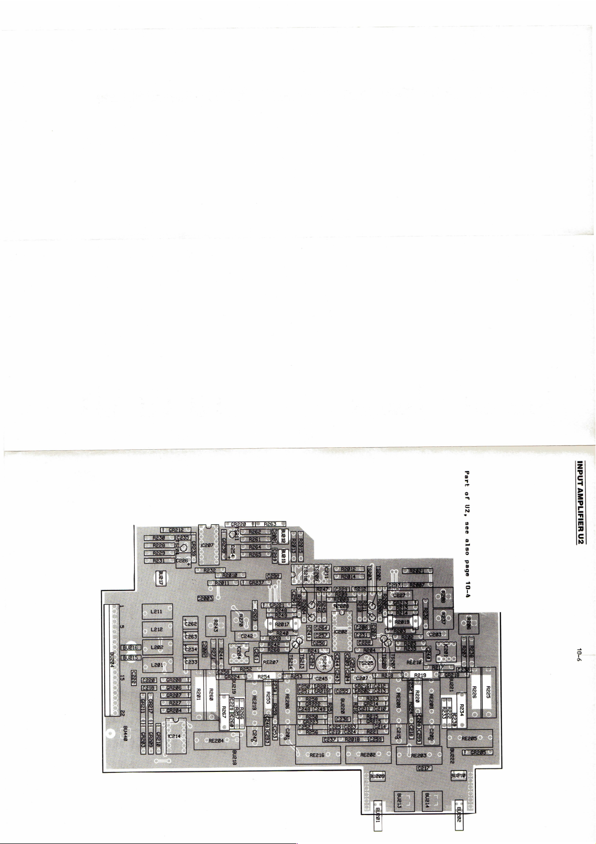
INPUT
AMPLIFIER
U2
10-6
 Loading...