

Philips PLHS501IA, PLHS501A Datasheet
474849505152
33323129 302827262524232221
234567
20
19
18
17
16
15
14
13
12
11
10
9
8
34
35
36
37
38
39
40
41
42
43
44
45
46
1
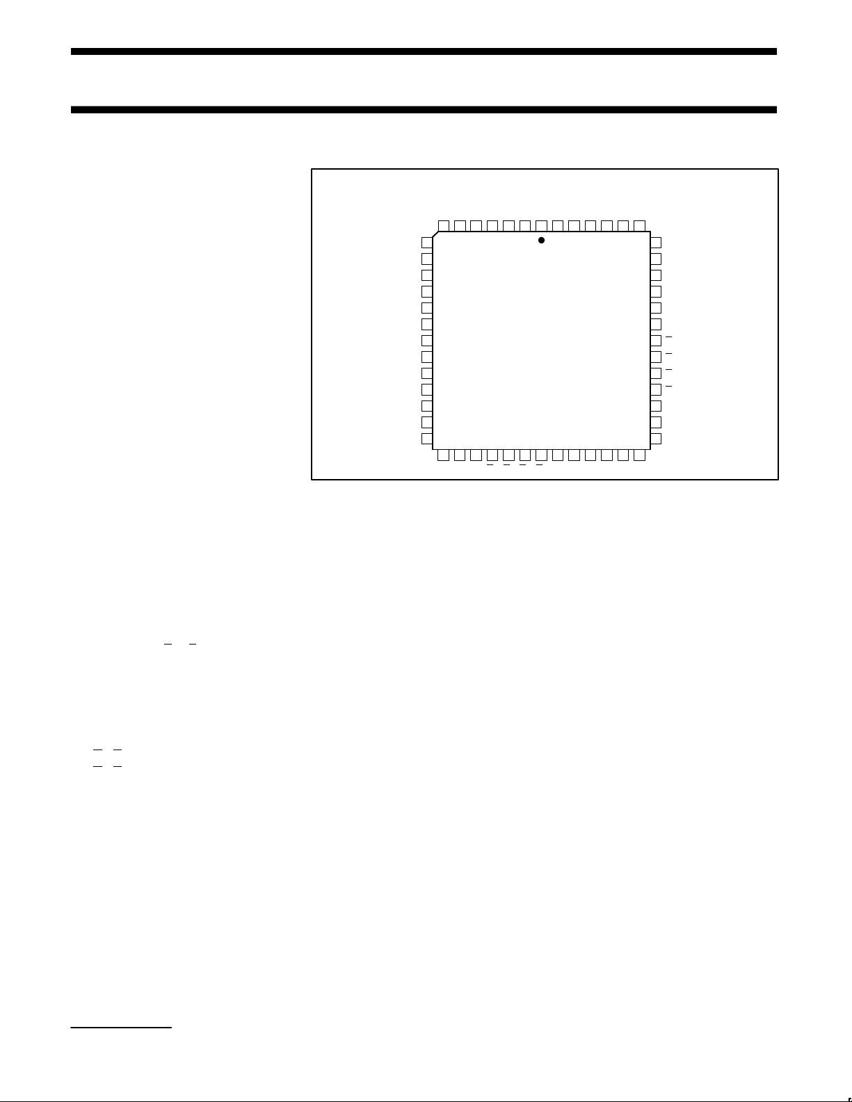
A Package
(52-pin PLCC)
I11I
12I10
I13I14I15I16I
17
I9I8I7I6I
5
V
CC
I
4
I
3
I
2
I
1
I
0
B
3
B
2
B
1
B
0
X
7
X
6
GNDGND
X
5X4X3X2X1X0O7O6O5O4O3O2O1
O
0
B
7
B
6
B
5
B
4
I
23
I
22
I
21
I
20
I
19
I
18
V
CC
Philips Semiconductors Programmable Logic Devices Product specification
PLHS501/PLHS501I
Programmable macro logic
PML
1
October 22, 1993 853–1207 11164
FEATURES
•Programmable Macro Logic device
•Full connectivity
•TTL compatible
•SNAP development system:
– Supports third-party schematic entry
formats
– Macro library
– Versatile netlist format for design
portability
– Logic, timing, and fault simulation
•Delay per internal NAND function = 6.5ns
(typ)
•Testable in unprogrammed state
•Security fuse allows protection of
proprietary designs
STRUCTURE
•NAND gate based architecture
– 72 foldback NAND terms
•136 input-wide logic terms
•44 additional logic terms
•24 dedicated inputs (I
0
– I23)
•8 bidirectional I/Os with individual 3-State
enable:
– 4 Active-High (B4 – B7)
– 4 Active-Low (B
0
– B3)
•16 dedicated outputs:
– 4 Active-High outputs
O
0
, O1 with common 3-State enable
O
2
, O3 with common 3-State enable
– 4 Active-Low outputs:
O4, O5 with common 3-State enable
O
6
, O7 with common 3-State enable
– 8 Exclusive-OR outputs:
X0, X1 with common 3-State enable
X
2
, X3 with common 3-State enable
X
4
, X5 with common 3-State enable
X
6
, X7 with common 3-State enable
PIN CONFIGURATION
DESCRIPTION
The PLHS501 is a high-density Bipolar
Programmable Macro Logic device. PML
incorporates a programmable NAND
structure. The NAND architecture is an
efficient method for implementing any logic
function. The SNAP software development
system provides a user friendly environment
for design entry. SNAP eliminates the need
for a detailed understanding of the PLHS501
architecture and makes it transparent to the
user. PLHS501 is also supported on the
Philips Semiconductors SNAP software
development systems.
The PLHS501 is ideal for a wide range of
microprocessor support functions, including
bus interface and control applications.
The PLHS501 is also processed to industrial
requirements for operation over an extended
temperature range of –40°C to +85°C and
supply voltage of 4.5V to 5.5V.
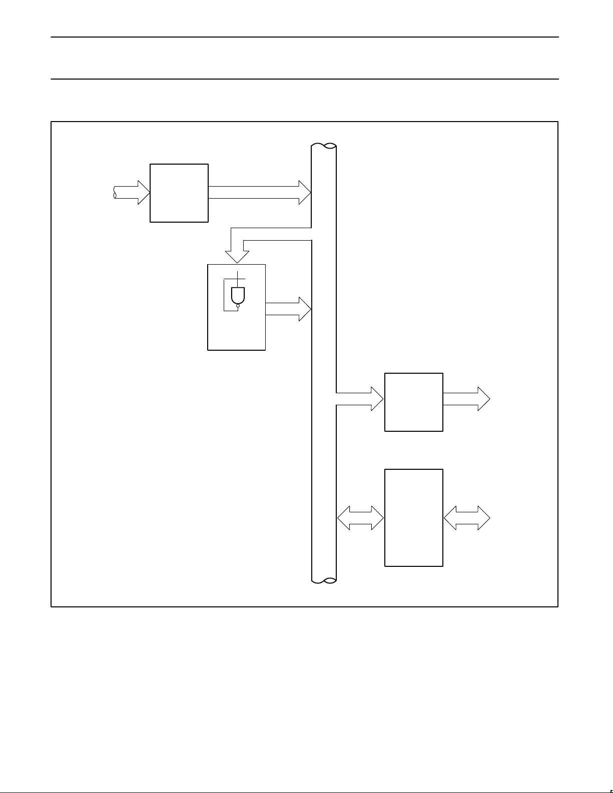
ARCHITECTURE
The core of the PLHS501 is a programmable
fuse array of 72 NAND gates. The output of
each gate folds back upon itself and all other
NAND gates. In this manner, full connectivity
of all logic functions is achieved in the
PLHS501. Any logic function can be created
within the core of the device without wasting
valuable I/O pins. Furthermore, a speed
advantage is acquired by implementing
multi-level logic within a fast internal core
without incurring any delays from the I/O
buffers.
PML is a trademark of Philips Semiconductors

Philips Semiconductors Programmable Logic Devices Product specification
PLHS501/PLHS501I
Programmable macro logic
PML
October 22, 1993
2
ORDERING INFORMATION
DESCRIPTION OPERATING CONDITIONS ORDER CODE DRAWING NUMBER
52-Pin Plastic Leaded Chip Carrier
Commercial Temperature Range
±5% Power Supply
PLHS501A 0397E
52-Pin Plastic Leaded Chip Carrier
Industrial Temperature Range
±10% Power Supply
PLHS501IA 0397E
DESIGN DEVELOPMENT TOOLS
SNAP
The SNAP Software Development System
provides the necessary tools for designing
with PML. SNAP provides the following:
•Schematic entry netlist generation from
third-party schematic design packages
such as OrCAD/SDT III
and
FutureNet
.
•Macro library for standard TTL functions
and user defined functions
•Boolean equation entry
•State equation entry
•Syntax and design entry checking
•Simulator includes logic simulation, fault
simulation and timing simulation.
SNAP operates on an IBM
PC/XT, PC/AT,
PS/2, or any compatible system with DOS
2.1 or higher. The minimum system
configuration for SNAP is 640K bytes of RAM
and a hard disk.
SNAP provides primitive PML function
libraries for third-party schematic design
packages. Custom macro function libraries
can be defined in schematic or equation form.
After the completion of a design, the software
compiles the design for syntax and
completeness. Complete simulation can be
carried out using the different simulation tools
available.
The programming data is generated in
JEDEC format. Using the Device
Programmer Interface (DPI) module of SNAP,
the JEDEC fusemap is sent from the host
computer to the device programmer.
DESIGN SECURITY
The PLHS501 has a programmable security
fuse that controls the access to the data
programmed in the device. By using this
programmable feature, proprietary designs
implemented in the device cannot be copied
or retrieved.
PROGRAMMING/SOFTWARE SUPPORT
Refer to Section 9
(Development Software)
and Section 10
(Third-party Programmer/
Software Support)
of this data handbook for
additional information.
FutureNet is a trademark of FutureNet Corporation.
OrCAD/SDT is a trademark of OrCAD, Inc.
IBM is a registered trademark of International Business Machines Corporation.
Philips Semiconductors Programmable Logic Devices Product specification
PLHS501/PLHS501I
Programmable macro logic
PML
October 22, 1993
3
PLHS501 FUNCTIONAL BLOCK DIAGRAM
I
N
T
E
R
C
O
N
N
E
C
T
24
DEDICATED
INPUTS
NAND
ARRAY
16
DEDICATED
OUTPUTS
8
BIDIRECTIONAL
I/OS
Philips Semiconductors Programmable Logic Devices Product specification
PLHS501/PLHS501I
Programmable macro logic
PML
October 22, 1993
4
FUNCTIONAL DIAGRAM
I
0
I
23
71 0
x4
x4
x4
x2
x2
B
0
– B
3
B4 – B
7
X0, X2, X4, X
6
X1, X3, X5, X
7
O0, O
2
O1, O
3
O4, O
6
O5, O
7
x4
x2
x2
x4x4x4x4x4x4x4x2x2x2x2x2x2
x4
DETAIL A
 Loading...