

Philips Plasma tv Service Manual

PLASMA TV
SERVICE MANUAL
PDF created with FinePrint pdfFactory trial version http://www.pdffactory.com

TABLE OF CONTENTS
1. INTRODUCTION.................................................................................................................................1
2. TUNER......................................................................................................................................................1
3. IF PART (TDA9886)...........................................................................................................................1
4. MULTI STANDARD SOUND PROCESSOR ..............................................................................2
5. 4.VIDEO SWITCH TEA6415............................................................................................................2
6. AUDIO AMPLIFIER STAGE WITH TDA7265.............................................................................2
7. POWER SUPPLY (SMPS)...............................................................................................................3
8. MICROCONTROLLER......................................................................................................................3
9. SERIAL ACCESS CMOS 4K x 8 (32K bit) EEPROM 24C32A..............................................3
10. CLASS AB STEREO HEADPHONE DRIVER TDA1308........................................................3
11. SAW FILTERS......................................................................................................................................3
12. IC DESCRIPTIONS AND INTERNAL BLOCK DIAGRAM......................................................4
12.1. MC44608............................................................................................................................................5
12.1.1. Description................................................................................................................................5
12.1.2. General Features ......................................................................................................................5
12.1.3. Pin Connections .......................................................................................................................5
12.2. TCET1102G.......................................................................................................................................6
12.2.1. Description................................................................................................................................6
12.2.2. Applications ..............................................................................................................................6
12.2.3. 13.12.3.Features........................................................................................................................6
12.3. TDA9886............................................................................................................................................6
12.3.1. General Description..................................................................................................................6
12.3.2. Features.....................................................................................................................................6
12.3.3. Pinning.......................................................................................................................................7
12.4. TEA6415C..........................................................................................................................................7
12.4.1. General Description..................................................................................................................7
12.4.2. Features.....................................................................................................................................7
12.4.3. Pinning.......................................................................................................................................8
12.5. SAA3010T..........................................................................................................................................8
12.5.1. Description................................................................................................................................8
12.5.2. Features.....................................................................................................................................8
12.5.3. Pinning.......................................................................................................................................8
12.6. 24C32A..............................................................................................................................................9
12.6.1. Features.....................................................................................................................................9
12.6.2. Description................................................................................................................................9
12.6.3. Pin Function table.....................................................................................................................9
12.6.4. Functional Descriptions.........................................................................................................10
12.7. SAA5264..........................................................................................................................................10
12.7.1. Features...................................................................................................................................10
12.7.2. General Description................................................................................................................10
12.7.3. Pin Connections and Short Descriptions.............................................................................10
12.8. LM317..............................................................................................................................................12
12.8.1. General Description................................................................................................................12
12.8.2. Features...................................................................................................................................12
12.9. ST24LC21........................................................................................................................................12
12.9.1. Description..............................................................................................................................12
12.9.2. Features...................................................................................................................................12
12.9.3. Pin connections......................................................................................................................13
12.10. TLC7733 ..........................................................................................................................................13
12.10.1. Description..............................................................................................................................13
12.11. 74LVC257A......................................................................................................................................14
12.11.1. Features...................................................................................................................................14
12.11.2. Description..............................................................................................................................14
12.11.3. Pin Description .......................................................................................................................14
12.12. 74LVC14A........................................................................................................................................14
i
Plasma TV Service Manual 24/10/2003
PDF created with FinePrint pdfFactory trial version http://www.pdffactory.com

12.12.1. Features...................................................................................................................................14
12.12.2. Applications ............................................................................................................................14
12.12.3. Description..............................................................................................................................14
12.12.4. Pin Description .......................................................................................................................15
12.13. TEA6420..........................................................................................................................................15
12.13.1. Features...................................................................................................................................15
12.13.2. Description..............................................................................................................................15
12.14. LM1086............................................................................................................................................15
12.14.1. Description..............................................................................................................................15
12.14.2. Features...................................................................................................................................15
12.14.3. Applications ............................................................................................................................16
12.14.4. Connection Diagrams.............................................................................................................16
12.15. LM1117............................................................................................................................................16
12.15.1. General Description................................................................................................................16
12.15.2. Features...................................................................................................................................16
12.15.3. Applications ............................................................................................................................16
12.15.4. Connection Diagrams.............................................................................................................16
12.16. DS90C385........................................................................................................................................17
12.16.1. General Description................................................................................................................17
12.16.2. Features...................................................................................................................................17
12.16.3. Pin Description .......................................................................................................................17
12.17. TL431...............................................................................................................................................18
12.17.1. Description..............................................................................................................................18
12.17.2. Features...................................................................................................................................18
12.17.3. Pin Configurations..................................................................................................................18
12.18. MSP34X1G......................................................................................................................................19
12.18.1. Introduction.............................................................................................................................19
12.18.2. Features...................................................................................................................................20
12.18.3. Pin connections......................................................................................................................20
12.19. TDA7265..........................................................................................................................................22
12.19.1. Description..............................................................................................................................22
12.19.2. Features...................................................................................................................................22
12.19.3. Pin Connection .......................................................................................................................22
12.20. TDA1308..........................................................................................................................................22
12.20.1. General Description................................................................................................................22
12.20.2. Features...................................................................................................................................22
12.20.3. Pinning.....................................................................................................................................23
12.21. PI5V330 ...........................................................................................................................................23
12.21.1. General Description................................................................................................................23
12.22. AD9883A..........................................................................................................................................23
12.22.1. General Description................................................................................................................23
12.22.2. Features...................................................................................................................................23
12.22.3. Pin Descriptions .....................................................................................................................24
12.23. SAA7118E........................................................................................................................................26
12.23.1. General Description................................................................................................................26
12.23.2. Features...................................................................................................................................27
12.23.3. Pinning.....................................................................................................................................28
12.24. TPS72501........................................................................................................................................32
12.24.1. General Description................................................................................................................32
12.24.2. Features...................................................................................................................................32
12.25. TSOP1836 .......................................................................................................................................33
12.25.1. Description..............................................................................................................................33
12.25.2. Features...................................................................................................................................33
12.26. PCF8591..........................................................................................................................................33
12.26.1. General Description................................................................................................................33
12.26.2. Features...................................................................................................................................33
12.26.3. Pinning.....................................................................................................................................34
12.27. PW1231 ...........................................................................................................................................34
12.27.1. General Description................................................................................................................34
12.27.2. Features...................................................................................................................................34
ii
Plasma TV Service Manual 24/10/2003
PDF created with FinePrint pdfFactory trial version http://www.pdffactory.com

12.27.3. Applications ............................................................................................................................35
12.28. PW181 .............................................................................................................................................35
12.28.1. General Description................................................................................................................35
12.28.2. Features...................................................................................................................................35
12.28.3. Applications ............................................................................................................................36
12.29. SIL151B ...........................................................................................................................................36
12.29.1. General Description................................................................................................................36
12.29.2. Features...................................................................................................................................36
12.30. SDRAM 4M x 16 (MT48LC4M16A2TG-75) .....................................................................................36
12.30.1. General Description................................................................................................................36
12.30.2. Features...................................................................................................................................37
12.30.3. Pin Descriptions .....................................................................................................................37
12.31. FLASH 8MBit ...................................................................................................................................39
12.31.1. Description..............................................................................................................................39
12.31.2. Features...................................................................................................................................39
13. SERVICE MENU SETTINGS ........................................................................................................40
13.1. display menu....................................................................................................................................40
13.2. calibration menu...............................................................................................................................42
13.3. deinterlacer menu ............................................................................................................................44
13.4. Service menu factory reset values...................................................................................................46
14. BLOCK DIAGRAM............................................................................................................................47
15. CIRCUIT DIAGRAMS ......................................................................................................................56
iii
Plasma TV Service Manual 24/10/2003
PDF created with FinePrint pdfFactory trial version http://www.pdffactory.com

1. INTRODUCTION
42” Plasma TV is a progressive TV control system with built-in de-interlacer and scaler. It uses a
852*480 panel with 16:9 aspect ratio.The TV is capable of operation in PAL, SECAM, NTSC (playback)
colour standards and multiple transmission standards as B/G, D/K, I/I’, and L/L´ including German and
NICAM stereo. Sound system output is supplying 2x14W (10%THD) for stereo 8Ω speakers. The
chassis is equipped with many inputs and outputs allowing it to be used as a center of a media system.
It supports following peripherals:
4 SCART’s with two of them supporting full SCART features including RGB input
2 AV inputs. (CVBS+ Stereo Audio)
1 SVHS iput
1 Streeo Headphone output
1 Subwoofer line level output
1 D-Sub 15 PC input
1 DVI input (Optional)
1 Stereo audio input for PC/DVI
1 LVDS connector for Plasma Display Connection
Other features include, 10 pg Teletext, Picture-In-Picture (PIP) , Picture-And-Picture (PAP) , PictureAnd-Text (PAT) and Picture Zoom.
2. TUNER
The tuners used in the design are combined VHF, UHF tuners suitable for CCIR systems B/G, H, L, L´,
I/I´, and D/K. The tuning is available through the digitally controlled I2C bus (PLL). Below you will find
info on one of the Tuners in use.
General description of UV1316:
The UV1316 tuner belongs to the UV 1300 family of tuners, which are designed to meet a wide range of
applications. It is a combined VHF, UHF tuner suitable for CCIR systems B/G, H, L, L’, I and I’. The low
IF output impedance has been designed for direct drive of a wide variety of SAW filters with sufficient
suppression of triple transient.
Features of UV1316:
1. Member of the UV1300 family small sized UHF/VHF tuners
2. Systems CCIR: B/G, H, L, L’, I and I’; OIRT: D/K
3. Digitally controlled (PLL) tuning via I2C-bus
4. Off-air channels, S-cable channels and Hyperband
5. World standardised mechanical dimensions and world standard pinning
6. Compact size
7. Complies to “CENELEC EN55020” and “EN55013”
Pinning:
1. Gain control voltage (AGC) : 4.0V, Max: 4.5V
2. Tuning voltage
3. I²C-bus address select : Max: 5.5V
4. I²C-bus serial clock : Min:-0.3V, Max: 5.5V
5. I²C-bus serial data : Min:-0.3V, Max: 5.5V
6. Not connected
7. PLL supply voltage : 5.0V, Min: 4.75V, Max: 5.5V
8. ADC input
9. Tuner supply voltage : 33V, Min: 30V, Max: 35V
10. Symmetrical IF output 1
11. Symmetrical IF output 2
3. IF PART (TDA9886)
The TDA9886 is an alignment-free multistandard (PAL, SECAM and NTSC) vision and sound IF signal PLL
Both devices can be used for TV, VTR, PC and set-top box applications.
The following figure shows the simplified block diagram of the integrated circuit.
The integrated circuit comprises the following functional blocks:
1
Plasma TV Service Manual 24/10/2003
PDF created with FinePrint pdfFactory trial version http://www.pdffactory.com
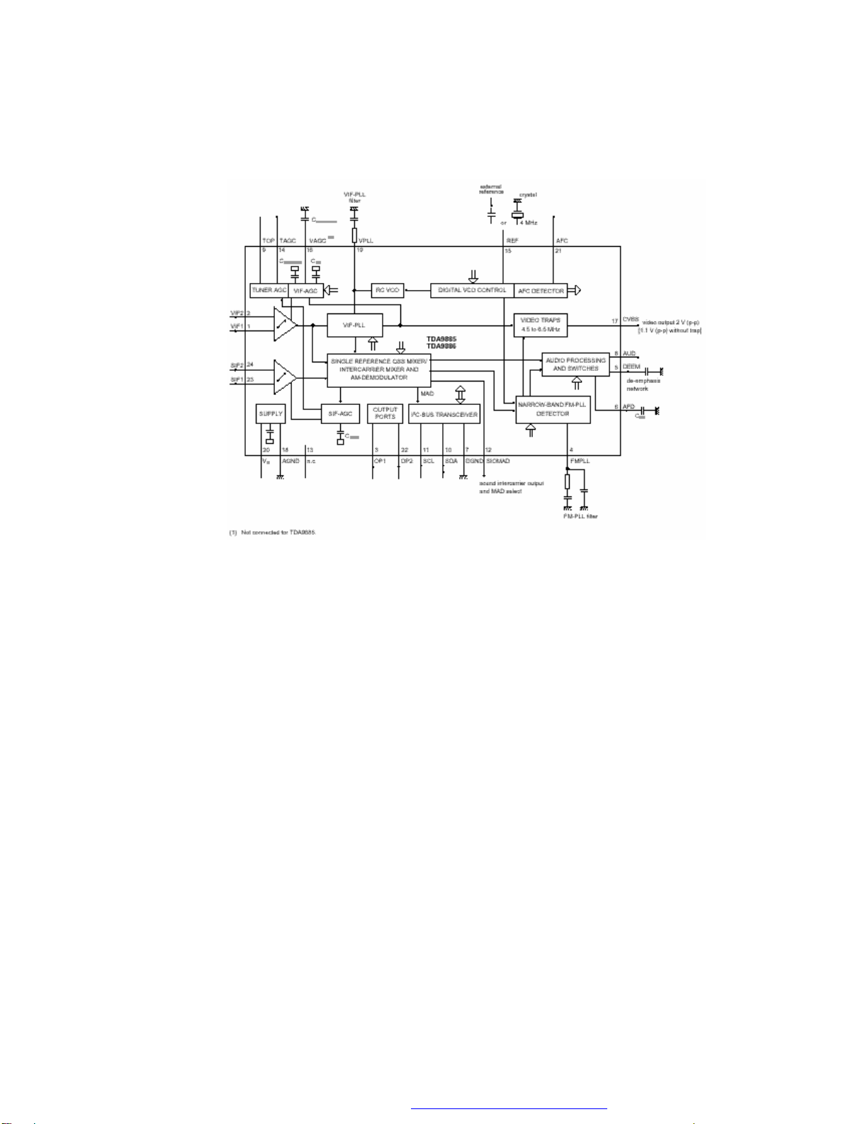
VIF amplifier, Tuner and VIF-AGC, VIF-AGC detector, Frequency Phase-Locked Loop (FPLL) detector, VCO
and divider, Digital acquisition help and AFC, Video demodulator and amplifier, Sound carrier trap, SIF
amplifier, SIF-AGC detector, Single reference QSS mixer, AM demodulator, FM demodulator and acquisition
help, Audio amplifier and mute time constant, I²C-bus transceivers and MAD (module address), Internal
voltage stabilizer.
4. MULTI STANDARD SOUND PROCESSOR
The MSP34x1G family of single-chip Multistandard Sound Processors covers the sound processing of
all analog TV-Standards worldwide, as well as the NICAM digital sound standards. The full TV sound
processing, starting with analog sound IF signal-in, down to processed analog AF-out, is performed on
a single chip.
These TV sound processing ICs include versions for processing the multichannel television sound
(MTS) signal conforming to the standard recommended by the Broadcast Television Systems
Committee (BTSC). The DBX noise reduction, or alternatively, Micronas Noise Reduction (MNR) is
performed alignment free. Other processed standards are the Japanese FM-FM multiplex standard
(EIA-J) and the FM Stereo Radio standard.
Current ICs have to perform adjustment procedures in order to achieve good stereo separation for
BTSC and EIA-J. The MSP34x1G has optimum stereo performance without any adjustments.
5. 4.VIDEO SWITCH TEA6415
In case of three or more external sources are used, the video switch IC TEA6415 is used. The main
function of this device is to switch 8 video-input sources on the 6 outputs.
Each output can be switched on only one of each input. On each input an alignment of the lowest level
of the signal is made (bottom of sync. top for CVBS or black level for RGB signals).
Each nominal gain between any input and output is 6.5dB.For D2MAC or Chroma signal the alignment
is switched off by forcing, with an external resistor bridge, 5VDC on the input. Each input can be used
as a normal input or as a MAC or Chroma input (with external Resistor Bridge). All the switching
possibilities are changed through the BUS. Driving 75ohm load needs an external resistor. It is possible
to have the same input connected to several outputs.
6. AUDIO AMPLIFIER STAGE WITH TDA7265
The TDA7265 is class AB dual Audio power amplifier assembled in the Multiwatt package, specially
designed for high quality sound application as Hi-Fi music centers and stereo TV sets.
2
Plasma TV Service Manual 24/10/2003
PDF created with FinePrint pdfFactory trial version http://www.pdffactory.com

7. POWER SUPPLY (SMPS)
The DC voltages required at various parts of the chassis are provided by an SMPS transformer
controlled by the IC MC44608, which is designed for driving, controlling and protecting switching
transistor of SMPS. The transformer generates 145V for FBT input, +/-14V for audio amplifier, 5V and
3.3V stand by voltage and 8V, 12V and 5V supplies for other different parts of the chassis.
An optocoupler is used to control the regulation of line voltage and stand-by power consumption. There
is a regulation circuit in secondary side. This circuit produces a control voltage according to the
changes in 145V DC voltage, via an optocoupler (TCET1102G) to pin3 of the IC.
During the switch on period of the transistor, energy is stored in the transformer. During the switch off
period energy is fed to the load via secondary winding. By varying switch-on time of the power
transistor, it controls each portion of energy transferred to the second side such that the output voltage
remains nearly independent of load variations.
8. MICROCONTROLLER
The microprocessor is embedded inside PW181 chip which also handles scaling, frame rate conversion
and OSD generation. The on-chip 16-bit microprocessor is a Turbo x86-compatible processor core with
on-chip peripherals (timers, interrupt controller, 2-wire serial master/slave interface, UART, I/O ports,
and more). Special peripherals such as Infrared (IR) pulse decoders and a digital pulse width modulator
(PWM) are also included. There are two independent 2-wire serial master/slave interface modules that
can be multiplexed to control up to five 2-wire serial ports. The slave 2-wire interface is designed for
HDCP use only (and requires the use of HDCP Image Processors). On-chip RAM of up to 64 Kbytes is
available. A complete microprocessor system can be implemented simply by adding external ROM. The
on-chip processor can be disabled to allow external processor control of all internal functions.
9. SERIAL ACCESS CMOS 4K x 8 (32K bit) EEPROM 24C32A
The Microchip Technology Inc. 24C32A is a 4K x 8 (32K bit) Serial Electrically Erasable PROM. It has
been developed for advanced, low power applications such as personal communications or data
acquisition. The 24C32A also has a page-write capability of up to 32 bytes of data. The 24C32A is
capable of both random and sequential reads up to the 32K boundary. Functional address lines allow
up to eight 24C32A devices on the same bus, for up to 256K bits address space. Advanced CMOS
technology and broad voltage range make this device ideal for low-power/low-voltage, non-volatile code
and data applications.
10. CLASS AB STEREO HEADPHONE DRIVER TDA1308
The TDA1308 is an integrated class AB stereo headphone driver contained in a DIP8 plastic package.
The device is fabricated in a 1 mm CMOS process and has been primarily developed for portable digital
audio applications.
11. SAW FILTERS
K9656M:
Standard:
• B/G
• D/K
• I
• L/L’
Features
• TV IF audio filter with two channels
• Channel 1 (L’) with one pass band for sound carriers at 40,40 MHz (L’) and 39,75 MHz (L’- NICAM)
• Channel 2 (B/G,D/K,L,I) with one pass band for sound carriers between 32,35 MHz and 33,40 MHz
Terminals
• Tinned CuFe alloy
Pin configuration
1 Input
2 Switching input
3 Chip carrier - ground
4 Output
5 Output
3
Plasma TV Service Manual 24/10/2003
PDF created with FinePrint pdfFactory trial version http://www.pdffactory.com

K3953M:
Standard:
• B/G
• D/K
• I
• L/L’
Features
TV IF video filter with Nyquist slopes at 33,90 MHz and 38,90 MHz
Constant group delay
Suitable for CENELEC EN 55020
Terminals
Tinned CuFe alloy
Pin configuration
1 Input
2 Input - ground
3 Chip carrier - ground
4 Output
5 Output
12. IC DESCRIPTIONS AND INTERNAL BLOCK DIAGRAM
MC44608
TCET1102G
TDA9886
TEA6415C
SAA3010T
24C32
SAA5264
LM317T
ST24LC21
TLC7733
74LVC257A
74LVC14A
TEA6420D
LM1086
LM1117
DS90C385
TL431
MSP3411G
TDA7265
TDA1308
PI5V330
AD9883A
SAA7118E
TPS72501
TSOP1836
PCF8591
PW1231
PW181
SIL151B
SDRAM 4M x 16 (MT48LC4M16A2TG-75)
FLASH
4
Plasma TV Service Manual 24/10/2003
PDF created with FinePrint pdfFactory trial version http://www.pdffactory.com

12.1. MC44608
12.1.1. Description
The MC44608 is a high performance voltage mode controller designed for off–line converters. This high
voltage circuit that integrates the start–up current source and the oscillator capacitor, requires few
external components while offering a high flexibility and reliability. The device also features a very high
efficiency stand–by management consisting of an effective Pulsed Mode operation. This technique
enables the reduction of the stand–by power consumption to approximately 1W while delivering 300mW
in a 150W SMPS.
• Integrated Start–Up Current Source
• Fast Start–Up
• Lossless Off–Line Start–Up
• Direct Off–Line Operation
12.1.2. General Features
• Flexibility
• Duty Cycle Control
• Under voltage Lockout with Hysteresis
• On Chip Oscillator Switching Frequency 40, or 75kHz
• Secondary Control with Few External Components
Protections
• Maximum Duty Cycle Limitation
• Cycle by Cycle Current Limitation
• Demagnetization (Zero Current Detection) Protection
• “Over VCC Protection” Against Open Loop
• Programmable Low Inertia Over Voltage Protection Against Open Loop
• Internal Thermal Protection
GreenLineTM Controller
• Pulsed Mode Techniques for a Very High Efficiency Low Power Mode
• Lossless Startup
• Low dV/dT for Low EMI Radiations
12.1.3. Pin Connections
Pin Name Description
1 Demag The Demag pin offers 3 different functions: Zero voltage crossing detection (50mV), 24mA current
2 ISENSE The Current Sense pin senses the voltage developed on the series resistor inserted in the source
3 Control Input A feedback current from the secondary side of the SMPS via the opto–coupler is injected into this
4 Ground This pin is the ground of the primary side of the SMPS.
5 Driver The current and slew rate capability of this pin are suited to drive Power MOSFETs.
6 VCC This pin is the positive supply of the IC. The driver output gets disabled when the voltage becomes
7 This pin is to provide isolation between the Vi pin 8 and the VCC pin 6.
8 Vi This pin can be directly connected to a 500V voltage source for start–up function of the IC. During
detection and 120mA current detection. The 24mA level is used to detect the secondary
reconfiguration status and the 120mA level to detect an Over Voltage status called Quick OVP.
of the power MOSFET. When I sense reaches 1V, the Driver output (pin 5) is disabled. This is
known as the Over Current Protection function. A 200mA current source is flowing out of the pin 3
during the start–up phase and during the switching phase in case of the Pulsed Mode of operation.
A resistor can be inserted between the sense resistor and the pin 3; thus a programmable peak
current detection can be performed during the SMPS stand–by mode.
pin. A resistor can be connected between this pin and GND to allow the programming of the Burst
duty cycle during the Stand–by mode.
higher than 15V and the operating range is between 6.6V and 13V. An intermediate voltage level
of 10V creates a disabling condition called Latched Off phase.
the Start–up phase a 9 mA current source is internally delivered to the VCC pin 6 allowing a rapid
charge of the VCC capacitor. As soon as the IC starts–up, this current source is disabled.
5
Plasma TV Service Manual 24/10/2003
PDF created with FinePrint pdfFactory trial version http://www.pdffactory.com

12.2. TCET1102G
12.2.1. Description
The TCET110/ TCET2100/ TCET4100 consists of a phototransistor optically coupled to a gallium
arsenide infrared-emitting diode in a 4-lead up to 16-lead plastic dual inline package. The elements are
mounted on one lead frame using a coplanar technique, providing a fixed distance between input and
output for highest safety requirements.
12.2.2. Applications
Circuits for safe protective separation against electrical shock according to safety class II (reinforced
isolation):
For appl. class I – IV at mains voltage ≤300 V
For appl. class I – III at mains voltage ≤600 V
According to VDE 0884, table 2, suitable for: Switch-mode power supplies, line receiver, computer
peripheral interface, microprocessor system interface.
12.2.3. 13.12.3.Features
VDE 0884 related features:
Rated impulse voltage (transient overvoltage) V IOTM = 8 kV peak
Isolation test voltage (partial discharge test voltage) V pd = 1.6 kV
Rated isolation voltage (RMS includes DC) V IOWM = 600 V RMS (848 V peak)
Rated recurring peak voltage (repetitive) V IORM = 600 V RMS
General features:
CTR offered in 9 groups
Isolation materials according to UL94-VO
Pollution degree 2 (DIN/VDE 0110 / resp. IEC 664)
Climatic classification 55/100/21 (IEC 68 part 1)
Special construction: Therefore, extra low coupling capacity of typical 0.2pF, high Common Mode
Rejection
Low temperature coefficient of CTR
G = Leadform 10.16 mm; provides creepage distance > 8 mm, for TCET2100/ TCET4100 optional;
suffix letter ‘G’ is not marked on the optocoupler
Coupling System U
12.3. TDA9886
12.3.1. General Description
The TDA9885 is an alignment-free single standard (without positive modulation) vision and sound IF signal
PLL.
12.3.2. Features
• 5 V supply voltage
• Gain controlled wide-band Vision Intermediate Frequency (VIF) amplifier (AC-coupled)
• Multistandard true synchronous demodulation with active carrier regeneration (very linear demodulation,
good intermodulation figures, reduced harmonics, excellent pulse response)
• Gated phase detector for L/L accent standard
• Fully integrated VIF Voltage Controlled Oscillator (VCO), alignment-free; frequencies switchable for all
negative and positive modulated standards via I2C-bus
• Digital acquisition help, VIF frequencies of 33.4, 33.9, 38.0, 38.9, 45.75 and 58.75 MHz
• 4 MHz reference frequency input [signal from Phase-Locked Loop (PLL) tuning system] or operating as
crystal oscillator
• VIF Automatic Gain Control (AGC) detector for gain control, operating as peak sync detector for negative
modulated signals and as a peak white detector for positive modulated signals
• Precise fully digital Automatic Frequency Control (AFC) detector with 4-bit digital-to-analog converter; AFC
bits via I2C -bus readable
6
Plasma TV Service Manual 24/10/2003
PDF created with FinePrint pdfFactory trial version http://www.pdffactory.com

• TakeOver Point (TOP) adjustable via I
2
C-bus or alternatively with potentiometer
• Fully integrated sound carrier trap for 4.5, 5.5, 6.0 and 6.5 MHz, controlled by FM-PLL oscillator
• Sound IF (SIF) input for single reference Quasi Split Sound (QSS) mode (PLL controlled)
• SIF AGC for gain controlled SIF amplifier; single reference QSS mixer able to operate in high performance
single reference QSS mode and in intercarrier mode, switchable via I2C-bus
• AM demodulator without extra reference circuit
• Alignment-free selective FM-PLL demodulator with high linearity and low noise
2
• I
C-bus control for all functions
2
• I
C-bus transceiver with pin programmable Module Address (MAD).
12.3.3. Pinning
SYMBOL PIN DESCRIPTION
VIF1 1
VIF2
OP1
FMPLL
DEEM
AFD
DGND
AUD
TOP
SDA
SCL
SIOMA
n.c.
TAGC
REF
VAGC
CVBS
AGND
VPLL
2
3
4
5
6
7
8
9
10
11
12
13
14
15
16
17
18
19
VP 20
AFC
OP2
SIF1
SIF2
21
22
23
24
VIF differential input 1
VIF differential input 2
output 1 (open-collector)
FM-PLL for loop filter
de-emphasis output for capacitor
AF decoupling input for capacitor
digital ground
audio output
tuner AGC TakeOver Point (TOP)
I2C-bus data input/output
I2C-bus clock input
sound intercarrier output and MAD select
not connected
tuner AGC output
4 MHz crystal or reference input
VIF-AGC for capacitor; note 1
video output
analog ground
VIF-PLL for loop filter
supply voltage (+5 V)
AFC output
output 2 (open-collector)
SIF differential input 1
SIF differential input 2
12.4. TEA6415C
12.4.1. General Description
The main function of the IC is to switch 8 video input sources on 6 outputs. Each output can be
switched on only one of each input. On each input an alignment of the lowest level of the signal is made
(bottom of synch. top for CVBS or black level for RGB signals). Each nominal gain between any input
and output is 6.5dB. For D2MAC or Chroma signal the alignment is switched off by forcing, with an
external resistor bridge, 5 VDC on the input. Each input can be used as a normal input or as a MAC or
Chroma input (with external resistor bridge). All the switching possibilities are changed through the
BUS. Driving 75Ω load needs an external transistor. It is possible to have the same input connected to
several outputs. The starting configuration upon power on (power supply: 0 to 10V) is undetermined. In
this case, 6 words of 16 bits are necessary to determine one configuration. In other case, 1 word of 16
bits is necessary to determine one configuration.
12.4.2. Features
• 20MHz Bandwidth
• Cascadable with another TEA6415C (Internal address can be changed by pin 7 voltage)
• 8 Inputs (CVBS, RGB, MAC, CHROMA,...)
• 6 Outputs
7
Plasma TV Service Manual 24/10/2003
PDF created with FinePrint pdfFactory trial version http://www.pdffactory.com

• Possibility of MAC or chroma signal for each input by switching-off the clamp with an external resistor
bridge
• Bus controlled
• 6.5dB gain between any input and output
• 55dB crosstalk at 5mHz
• Fully ESD protected
12.4.3. Pinning
1. Input : Max : 2Vpp, Input Current: 1mA, Max : 3mA
2. Data : Low level : -0.3V Max: 1.5V,
High level : 3.0V Max : Vcc+0.5V
3. Input : Max : 2Vpp, Input Current: 1mA, Max : 3mA
4. Clock : Low level : -0.3V Max: 1.5V,
High level : 3.0V Max : Vcc+0.5V
5. Input : Max : 2Vpp, Input Current: 1mA, Max : 3mA
6. Input : Max : 2Vpp, Input Current: 1mA, Max : 3mA
7. Prog
8. Input : Max : 2Vpp, Input Current: 1mA, Max: 3mA
9. Vcc : 12V
10. Input : Max : 2Vpp, Input Current: 1mA, Max : 3mA
11. Input : Max : 2Vpp, Input Current: 1mA, Max : 3mA
12. Ground
13. Output : 5.5Vpp, Min : 4.5Vpp
14. Output : 5.5Vpp, Min : 4.5Vpp
15. Output : 5.5Vpp, Min : 4.5Vpp
16. Output : 5.5Vpp, Min : 4.5Vpp
17. Output : 5.5Vpp, Min : 4.5Vpp
18. Output : 5.5Vpp, Min : 4.5Vpp
19. Ground
20. Input : Max : 2Vpp, Input Current : 1mA, Max : 3mA
12.5. SAA3010T
12.5.1. Description
The SAA3010 is intended as a general purpose (RC-5) infrared remote control system for use where a low
voltage supply and a large debounce time are expected. The device can generate 2048 different commands
and utilizes a keyboard with a single pole switch for each key. The commands are arranged so that 32
systems can be addressed, each system containing 64 different commands. The circuit response to legal
(one key pressed at a time) and illegal (more than one key pressed at a time) keyboard operation is specified
in the section “Keyboard operation”.
12.5.2. Features
Low voltage requirement
Biphase transmission technique
Single pin oscillator
Test mode facility
12.5.3. Pinning
Pin Mnemonic Function
1 X7 (IPU) sense input from key matrix
2 SSM (I) sense mode selection input
3 Z0-Z3 (IPU) sense inputs from key matrix
7 MDATA (OP3) generated output data modulated with 1/12 the oscillator frequency at a 25% duty factor
8 DATA (OP3) generated output information
9-13 DR7-DR3 (ODN) Scan drivers
14 VSS Ground (0V)
15-17 DR-2-DR0 (ODN) Scan drivers
18 OSC (I) Oscillator input
8
Plasma TV Service Manual 24/10/2003
PDF created with FinePrint pdfFactory trial version http://www.pdffactory.com

19 TP2 (I) test point 2
20 TP1 (I) Test point 1
21-27 X0-X6 (IPU) Sense inputs from key matrix
28 VDD(I) Voltage supply
Note:
(I): Input,
(IPU): input with p-channel pull-up transistor,
(ODN): output with open drain n-channel transistor
(OD3): output 3-state
12.6. 24C32A
12.6.1. Features
• Voltage operating range: 4.5V to 5.5V
- Maximum write current 3 mA at 5.5V
- Standby current 1 mA typical at 5.0V
• 2-wire serial interface bus, I2CTM compatible
• 100 kHz and 400 kHz compatibility
• Self-timed ERASE and WRITE cycles
• Power on/off data protection circuitry
• Hardware write protect
• 1,000,000 Erase/Write cycles guaranteed
• 32-byte page or byte write modes available
• Schmitt trigger filtered inputs for noise suppression
• Output slope control to eliminate ground bounce
• 2 ms typical write cycle time, byte or page
• Up to eight devices may be connected to the same bus for up to 256K bits total memory
• Electrostatic discharge protection > 4000V
• Data retention > 200 years
• 8-pin PDIP and SOIC packages
• Temperature ranges
- Commercial (C): 0°C to 70°C
- Industrial (I): -40°C to +85°C
- Automotive (E): -40°C to +125°C
12.6.2. Description
The Microchip Technology Inc. 24C32A is a 4K x 8 (32K bit) Serial Electrically Erasable PROM. It has
been developed for advanced, low power applications such as personal communications or data
acquisition. The 24C32A also has a page-write capability of up to 32 bytes of data. The 24C32A is
capable of both random and sequential reads up to the 32K boundary. Functional address lines allow
up to eight 24C32A devices on the same bus, for up to 256K bits address space. Advanced CMOS
technology and broad voltage range make this device ideal for low-power/low-voltage, non-volatile code
and data applications. The 24C32A is available in the standard 8-pin plastic DIP and both 150 mil and
200 mil SOIC packaging.
12.6.3. Pin Function table
Name Function
A0, A1, A2 User Configurable Chip Selects
Vss Ground
SDA Serial Address/Data I/O
SCL Serial Clock
WP Write Protect Input
Vcc +4.5V to 5.5V Power Supply
9
Plasma TV Service Manual 24/10/2003
PDF created with FinePrint pdfFactory trial version http://www.pdffactory.com
12.6.4. Functional Descriptions
The 24C32A supports a Bi-directional 2-wire bus and data transmission protocol. A device that sends
data onto the bus is defined as transmitter, and a device receiving data as receiver. The bus must be
controlled by a master device which generates the Serial Clock (SCL), controls the bus access, and
generates the START and STOP conditions, while the 24C32A works as slave. Both master and slave
can operate as transmitter or receiver but the master device determines which mode is activated.
12.7. SAA5264
12.7.1. Features
The following features apply to both SAA5264 and SAA5265:
• Complete 625 line teletext decoder in one chip reduces printed circuit board area and cost
• Automatic detection of transmitted fastext links or service information (packet 8/30)
• On-Screen Display (OSD) for user interface menus using teletext and dedicated menu icons
• Video Programming System (VPS) decoding
• Wide Screen Signalling (WSS) decoding
• Pan-European, Cyrillic, Greek/Turkish and French/Arabic character sets in each chip
• High-level command interface via I
2
C-bus gives easy control with a low software overhead
• High-level command interface is backward compatible to Stand-Alone Fastext And Remote Interface
(SAFARI)
• 625 and 525 line display
• RGB interface to standard colour decoder ICs, current source
• Versatile 8-bit open-drain Input/Output (I/O) expander, 5 V tolerant
• Single 12 MHz crystal oscillator
• 3.3 V supply voltage.
SAA5264 features
• Automatic detection of transmitted pages to be selected by page up and page down
• 8 Page fastext decoder
• Table Of Pages (TOP) decoder with Basic Top Table (BTT) and Additional Information Tables (AITs)
• 4 Page user-defined list mode.
12.7.2. General Description
The SAA5264 is a single-chip ten page 625-line World System Teletext decoder with a high-level
command interface, and is SAFARI compatible.
The device is designed to minimize the overall system cost, due to the high-level command interface
offering the benefit of a low software overhead in the TV microcontroller.
The SAA5264 has the following functionality:
• 10 page teletext decoder with OSD, Fastext, TOP, default and list acquisition modes
• Automatic channel installation support
• Closed caption acquisition and display
• Violence Chip (VChip) support.
12.7.3. Pin Connections and Short Descriptions
SYMBOL PIN TYPE DESCRIPTION
Port 2: 8-bit programmable bidirectional port with alternative functions
P2.0/PWM 1 I/O
P2.1/PWM0 2 I/O
P2.2/PWM1 3 I/O
P2.3/PWM2 4 I/O
P2.4/PWM3 5 I/O
P2.5/PWM4 6 I/O
P2.6/PWM5 7 I/O
P2.7/PWM6 8 I/O
Port 3: 8-bit programmable bidirectional port with alternative functions
P3.0/ADC0
P3.1/ADC1
9 I/O
10 I/O
output for 14-bit high precision Pulse Width Modulator (PWM)
outputs for 6-bit PWMs 0 to 6
inputs for the software Analog-to-Digital-Converter (ADC) facility
10
Plasma TV Service Manual 24/10/2003
PDF created with FinePrint pdfFactory trial version http://www.pdffactory.com

P3.2/ADC2
P3.3/ADC3
P3.4/PWM7
V
SSC
11 I/O
12 I/O
30 I/O
13 I/O
output for 6-bit PWM7
core ground
Port 0: 8-bit programmable bidirectional port
SCL(NVRAM)
SDA(NVRAM)
P0.2
P0.3
P0.4
P0.5
14 I
15 I/O
16 I/O
17 I/O
18 I/O
19 I/O
I2C-bus Serial Clock input to Non-Volatile RAM
I2C-bus Serial Data input/output (Non-Volatile RAM)
input/output for general use
input/output for general use
input/output for general use
8 mA current sinking capability for direct drive of Light Emitting
Diodes (LEDs)
P0.6
P0.7
V
22 -
SSA
CVBS0
20 I/O
21 I/O
23 I
input/output for general use
analog ground
Composite Video Baseband Signal (CVBS) input; a positive-going
1V
CVBS1
SYNC_FILTER
24 I
25 I sync-pulse-filter input for CVBS; this pin should be connected to V
(peak-to-peak) input is required; connected via a 100 nF capacitor
via a 100 nF capacitor
IREF
26 I
reference current input for analog circuits; for correct operation a 24
κΩ resistor should be connected to V
FRAME
27 O
Frame de-interlace output synchronized with the VSYNC pulse to
produce a non-interlaced display by adjustment of the vertical
deflection circuits
TEST
COR
28 I not available; connect this pin to V
29 O
contrast reduction: open-drain, active LOW output which allows
selective contrast reduction of the TV picture to enhance a mixed
mode display
V
31 -
DDA
B
G
R
VDS
HSYNC
30 I/O
32 O
33 O
34 O
35 O
36 I
P3.4/PWM7 (described above)
analog supply voltage (3.3 V)
Blue colour information pixel rate output
Green colour information pixel rate output
Red colour information pixel rate output
video/data switch push-pull output for pixel rate fast blanking
horizontal sync pulse input: Schmitt triggered for a Transistor
Transistor Level (TTL) version; the polarity of this pulse is
programmable by register bit TXT1.H POLARITY
VSYNC
37 I
vertical sync pulse input; Schmitt triggered for a TTL version; the
polarity of this pulse is programmable by register bit TXT1.V
POLARITY
V
SSP
V
DDC
OSCGND
XTALIN
XTALOUT
RESET
38 39 40 -*
41 I
42 O
43 I
periphery ground
core supply voltage (+3.3 V)
crystal oscillator ground
12 MHz crystal oscillator input
12 MHz crystal oscillator output
reset input; if this pin is HIGH for at least 2 machine cycles (24
oscillator periods) while the oscillator is running, the device resets;
this pin should be connected to V
V
DDP
44 -
periphery supply voltage (+3.3 V)
Port 1: 8-bit programmable bidirectional port
P1.0
P1.1
P1.2
P1.3
SCL
45 I/O
46 I/O
47 I/O
48 I/O
49 I
input/output for general use
input/output for general use
input/output for general use
input/output for general use
I2C-bus Serial Clock input from application
SSA
SSA
via a capacitor
DDP
SSA
11
Plasma TV Service Manual 24/10/2003
PDF created with FinePrint pdfFactory trial version http://www.pdffactory.com

SDA
P1.4
P1.5
50 I/O
51 I/O
52 I/O
I2C-bus Serial Data input from (application)
input/output for general use
input/output for general use
12.8. LM317
12.8.1. General Description
The LM117/LM217/LM317 are monolithic integrated circuit in TO-220, ISOWATT220, TO-3 and D 2
PAK packages intended for use as positive adjustable voltage regulators.
They are designed to supply more than 1.5A of load current with an output voltage adjustable over a
1.2 to 37V range.
The nominal output voltage is selected by means of only a resistive divider, making the device
exceptionally easy to use and eliminating the stocking of many fixed regulators.
12.8.2. Features
• Output voltage range : 1.2 To 37V
• Output current In excess of 1.5A
• 0.1% Line and Load Regulation
• Floating Operation for High Voltages
• Complete Series of Protections : Current Limiting, Thermal Shutdown And Soa Control
12.9. ST24LC21
12.9.1. Description
The ST24LC21 is a 1K bit electrically erasable programmable memory (EEPROM), organized by 8 bits.
This device can operate in two modes: Transmit Only mode and I2C bidirectional mode. When powered,
the device is in Transmit Only mode with EEPROM data clocked out from the rising edge of the signal
applied on VCLK. The device will switch to the I2C bidirectional mode upon the falling edge of the signal
applied on SCL pin. The ST24LC21 can not switch from the I2C bidirectional mode to the Transmit Only
mode (except when the power supply is removed). The device operates with a power supply value as
low as 2.5V. Both Plastic Dual-in-Line and Plastic Small Outline packages are available.
12.9.2. Features
• 1 million Erase/Write cycles
• 40 years data retention
• 2.5V To 5.5V single supply voltage
• 400k Hz compatibility over the full range of supply voltage
• Two wire serial interface I2C bus compatible
• Page Write (Up To 8 Bytes)
• Byte, random and sequential read modes
• Self timed programming cycle
• Automatic address incrementing
• Enhanced ESD/Latch up
• Performances
12
Plasma TV Service Manual 24/10/2003
PDF created with FinePrint pdfFactory trial version http://www.pdffactory.com

12.9.3. Pin connections
DIP Pin connections CO Pin connections
NC: Not connected
Signal names
SDA Serial data Address Input/Output
SCL Serial Clock (I2C mode)
Vcc Supply voltage
Vss Ground
VCLK Clock transmit only mode
12.10. TLC7733
12.10.1. Description
The TLC77xx family of micropower supply voltage supervisors are designed for reset control, primarily
in microcomputer and microprocessor systems.
During power-on, RESET is asserted when V
reaches 1 V. After minimum V
DD
(. 2 V) is established,
DD
the circuit monitors SENSE voltage and keeps the reset outputs active as long as SENSE voltage
(V
I(SENSE)
)
remains below the threshold voltage. An internal timer delays return of the output to the inactive state to
ensure proper system reset. The delay time, td, is determined by an external capacitor:
t
= 2.1 x 10 4 x CT
d
where
C
is in farads
T
td is in seconds
The TLC77xx has a fixed SENSE threshold voltage set by an internal voltage divider. When SENSE
voltage drops below the threshold voltage, the outputs become active and stay in that state until
SENSE voltage returns above threshold voltage and the delay time, td, has expired.
In addition to the power-on-reset and undervoltage-supervisor function, the TLC77xx adds power-down
control support for static RAM. When CONTROL is tied to GND, RESET will act as active high. The
voltage monitor contains additional logic intended for control of static memories with battery backup
during power failure. By driving the chip select (CS) of the memory circuit with the RESET output of the
TLC77xx and with the CONTROL driven by the memory bank select signal (CSH1) of the
microprocessor (see Figure 10), the memory circuit is automatically disabled during a power loss. (In
this application the TLC77xx power has to be supplied by the battery.)
The TLC77xxQ is characterized for operation over a temperature range of –40°C to 125°C, and the
TLC77xxI is characterized for operation over a temperature range of –40°C to 85°C.
13
Plasma TV Service Manual 24/10/2003
PDF created with FinePrint pdfFactory trial version http://www.pdffactory.com

12.11. 74LVC257A
12.11.1. Features
Wide supply voltage range of 1.2 to 3.6 V
In accordance with JEDEC standard no. 8-1A
CMOS lower power consumption
Direct interface with TTL levels
Output drive capability 50 _ transmission lines at 85°C
5 Volt tolerant inputs/outputs, for interfacing with 5 Volt logic
12.11.2. Description
The 74LVC257A is a high-performance, low-power, low-voltage, Si-gate CMOS device and superior to
most advanced CMOS compatible TTL families.
Inputs can be driven from either 3.3V or 5.0V devices. In 3-State operation, outputs can handle 5V. This
feature allows the use of these devices as translators in a mixed 3.3V/5V environment.
The 74LVC257A is a quad 2-input multiplexer with 3-state outputs, which select 4 bits of data from two
sources and are controlled by a common data select input (S). The data inputs from source 0 (1l 0 to 4l
0 ) are selected when input S is LOW and the data inputs from source 1 (1l 1 to 4l 1 ) are selected
when S in HIGH. Data appears at the outputs (1Y to 4Y) in true (non-inverting) form from the selected
inputs. The 74LVC257A is the logic implementation of a 4-pole, 2-position switch, where the position of
the switch is determined by the logic levels applied to S. The outputs are forced to a high impedance
OFF-state when OE is HIGH.
12.11.3. Pin Description
PIN NUMBER SYMBOL DESCRIPTION
1 S Common data select input
2, 5, 11, 14
3, 6, 10, 13
4,7,9,12 1Y to 4Y 3-State multiplexer outputs
8 GND Ground (0V)
15 OE 3-State output enable input (active LOW)
16 Vcc Positive supply voltage
1|0 to 4|0
1|1 to 4|1
Data inputs from source 0
Data outputs from source 1
12.12. 74LVC14A
12.12.1. Features
• Wide supply voltage range of 1.2 to 3.6 V
• In accordance with JEDEC standard no. 8-1A
• Inputs accept voltages up to 5.5 V
• CMOS low power consumption
• Direct interface with TTL levels
12.12.2. Applications
• Wave and pulse shapers for highly noisy environments
• Astable multivibrators
• Monostable multivibrators
12.12.3. Description
The 74LVC14A is a high-performance, low power, low-voltage Si-gate CMOS device and superior to
most advanced CMOS compatible TTL families.
Inputs can be driven from either 3.3 V or 5 V devices. This feature allows the use of these devices as
translators in a mixed 3.3 V/5 V environment.
The 74LVC14A provides six inverting buffers with Schmitt-trigger action. It is capable of transforming
slowly changing input signals into sharply defined, jitter-free output signals.
14
Plasma TV Service Manual 24/10/2003
PDF created with FinePrint pdfFactory trial version http://www.pdffactory.com

12.12.4. Pin Description
PIN NUMBER SYMBOL DESCRIPTION
1, 3, 5, 9, 11, 13 1A – 6A Data inputs
2, 4, 6, 8, 10, 12 1Y – 6Y Data outputs
7 GND Ground (0V)
14 Vcc Positive supply voltage
12.13. TEA6420
12.13.1. Features
• 5 Stereo Inputs
• 4 Stereo Ouputs
• Gain Control 0/2/4/6db/Mutefor EachOutput
• Cascadable (2 Different Addresses)
• Serial Bus Controlled
• Very Low noise
• Very Low distorsion
12.13.2. Description
The TEA6420 switches 5 stereo audio inputs on 4 stereo outputs.
All the switching possibilities are changed through the I2C bus.
12.14. LM1086
12.14.1. Description
The LM1086 is a series of low dropout positive voltage regulators with a maximum dropout of 1.5V at
1.5A of load current. It has the same pin-out as National Semiconductor’s industry standard LM317.
The LM1086 is available in an adjustable version, which can set the output voltage with only two
external resistors. It is also available in five fixed voltages: 2.5V, 2.85V, 3.3V, 3.45V and 5.0V. The fixed
versions integrate the adjust resistors. The LM1086 circuit includes a zener trimmed band-gap
reference, current limiting and thermal shutdown.
12.14.2. Features
• Available in 2.5V, 2.85V, 3.3V, 3.45V, 5V and Adjustable Versions
• Current Limiting and Thermal Protection
• Output Current 1.5A
• Line Regulation 0.015% (typical)
• Load Regulation 0.1% (typical)
Plasma TV Service Manual 24/10/2003
15
PDF created with FinePrint pdfFactory trial version http://www.pdffactory.com
12.14.3. Applications
• SCSI-2 Active Terminator
• High Efficiency Linear Regulators
• Battery Charger
• Post Regulation for Switching Supplies
• Constant Current Regulator
• Microprocessor Supply
12.14.4. Connection Diagrams
12.15. LM1117
12.15.1. General Description
The LM1117 is a series of low dropout voltage regulators with a dropout of 1.2V at 800mA of load
current. It has the same pin-out as National Semiconductor’s industry standard LM317. The LM1117 is
available in an adjustable version, which can set the output voltage from 1.25V to 13.8V with only two
external resistors. In addition, it is also available in five fixed voltages, 1.8V, 2.5V, 2.85V, 3.3V, and 5V.
The LM1117 offers current limiting and thermal shutdown. Its circuit includes a zener trimmed bandgap
reference to as-sure output voltage accuracy to within ±1%. The LM1117 series is available in SOT223, TO-220, and TO-252 D-PAK packages. A minimum of 10µF tantalum capacitor is required at the
output to improve the transient response and stability.
12.15.2. Features
• Available in 1.8V, 2.5V, 2.85V, 3.3V, 5V, and Adjustable Versions
• Space Saving SOT-223 Package
• Current Limiting and Thermal Protection
• Output Current 800mA
• Line Regulation 0.2% (Max)
• Load Regulation 0.4% (Max)
• Temperature Range
— LM1117 0°C to 125°C
— LM1117I -40°C to 125°C
12.15.3. Applications
• 2.85V Model for SCSI-2 Active Termination
• Post Regulator for Switching DC/DC Converter
• High Efficiency Linear Regulators
• Battery Charger
• Battery Powered Instrumentation
12.15.4. Connection Diagrams
16
Plasma TV Service Manual 24/10/2003
PDF created with FinePrint pdfFactory trial version http://www.pdffactory.com
 Loading...