

Philips PIMT1 Datasheet
DISCRETE SEMICONDUCTORS
DATA SH EET
ook, halfpage
M3D302
PIMT1
PNP general purpose double
transistor
Product specification 2001 Oct 22

Philips Semiconductors Product specification
PNP general purpose double transistor PIMT1
FEATURES
• 600 mW total power dissipation
• Low current (max. 100 mA)
• Low voltage (max. 40 V)
• Reduces number of components and required
PCB area
• Reduced pick and place costs.
APPLICATIONS
• General purpose switching and amplification.
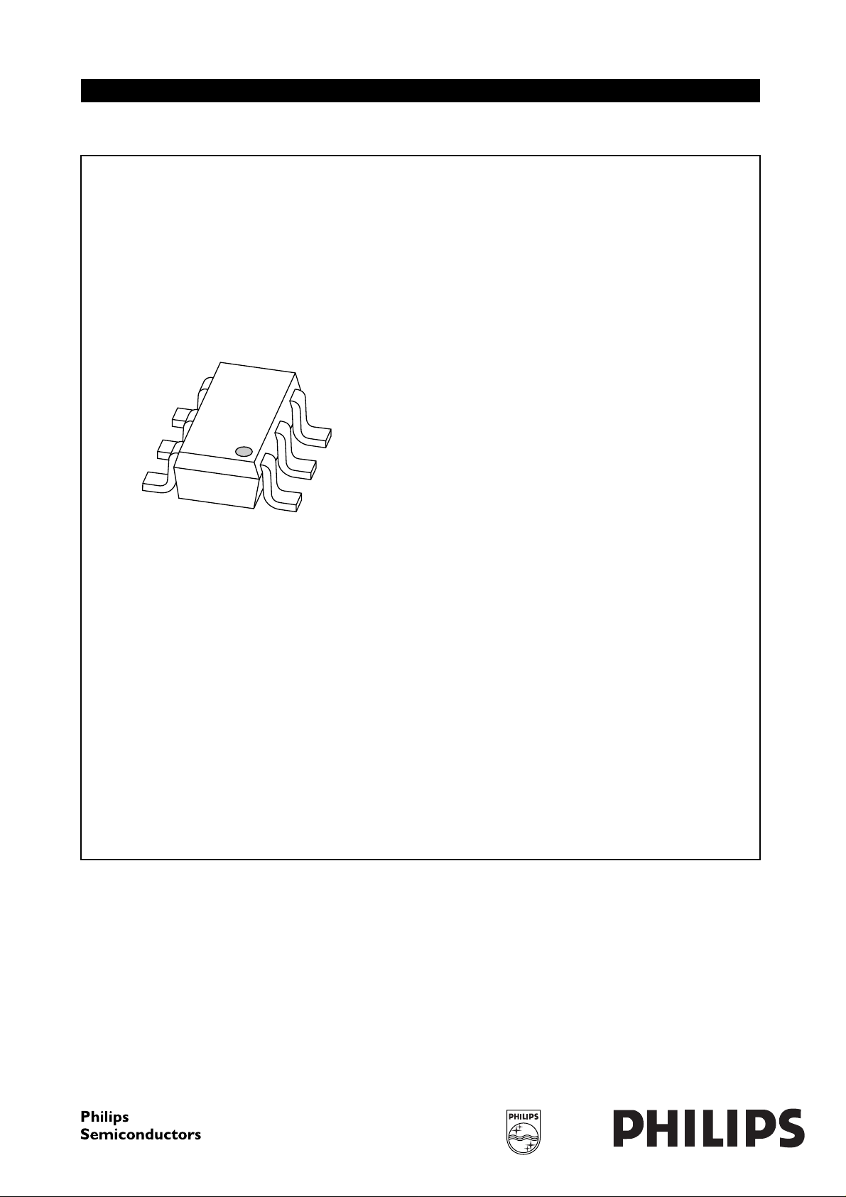
DESCRIPTION
PNP transistor pair in an SC-74 (SOT457) plastic
package.
MARKING
TYPE NUMBER MARKING CODE
PIMT1 M1
PINNING
PIN DESCRIPTION
1, 4 emitter TR1; TR2
2, 5 base TR1; TR2
6, 3 collector TR1; TR2
654
123
Top view
MAM457
645
TR1
132
Fig.1 Simplified outline (SC74; SOT457) and
symbol.
TR2
LIMITING VALUES
In accordance with the Absolute Maximum Rating System (IEC 60134).
SYMBOL PARAMETER CONDITIONS MIN. MAX. UNIT
Per transistor
V
CBO
V
CEO
V
EBO
I
C
I
CM
I
BM
P
tot
T
stg
T
j
T
amb
collector-base voltage open emitter −−50 V
collector-emitter voltage open base −−40 V
emitter-base voltage open collector −−5V
collector current (DC) −−100 mA
peak collector current −−200 mA
peak base current −−200 mA
total power dissipation T
≤ 25 °C; note 1 − 300 mW
amb
storage temperature −65 +150 °C
junction temperature − 150 °C
operating ambient temperature −65 +150 °C
Per device
P
tot
total power dissipation T
≤ 25 °C; note 1 − 600 mW
amb
Note
1. Device mounted on a printed-circuit board, single sided copper, tinplated and mounting pad for collector 1 cm2.
2001 Oct 22 2
Philips Semiconductors Product specification
PNP general purpose double transistor PIMT1
THERMAL CHARACTERISTICS
SYMBOL PARAMETER CONDITIONS VALUE UNIT
R
th j-a
Note
1. Device mounted on a printed-circuit board, single sided copper, tinplated and mounting pad for collector 1 cm
CHARACTERISTICS
T
=25°C unless otherwise specified.
amb
SYMBOL PARAMETER CONDITIONS MIN. MAX. UNIT
Per transistor
I
CBO
I
EBO
h
FE
V
CEsat
C
c
f
T
thermal resistance from junction to ambient note 1 208 K/W
collector-base cut-off current VCB= −30 V; IE=0 −−100 nA
V
= −30 V; IE= 0; Tj= 150 °C −−10 µA
CB
emitter-base cut-off current VEB= −4 V; IC=0 −−100 nA
DC current gain VCE= −6 V; IC= −1 mA 120 −
collector-emitter saturation
IC= −50 mA; IB= −5 mA; note 1 −−200 mV
voltage
collector capacitance VCB= −12 V; IE=Ie= 0; f = 1 MHz − 2.2 pF
transition frequency VCE= −12 V; IC= −2 mA;
100 − MHz
f = 100 MHz
2
.
Note
1. Pulse test: t
≤ 300 µs; δ≤0.02.
p
2001 Oct 22 3
 Loading...