

Philips PHX4ND40E Datasheet
Philips Semiconductors Product specification
PowerMOS transistors PHX4ND40E
FREDFET, Avalanche energy rated
FEATURES SYMBOL QUICK REFERENCE DATA
• Repetitive Avalanche Rated V
d
• Fast switching
• Stable off-state characteristics I
• High thermal cycling performance
• Isolated package R
g
• Fast reverse recovery diode
s
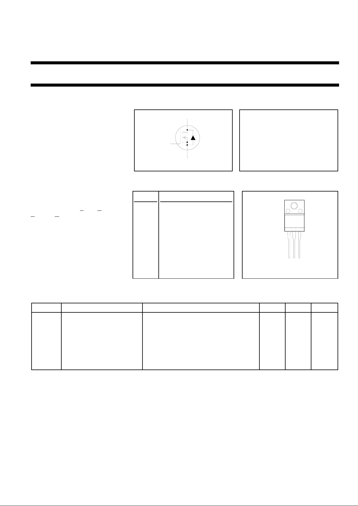
GENERAL DESCRIPTION PINNING SOT186A
N-channel, enhancement mode PIN DESCRIPTION
field-effect power transistor,
incorporating a Fast Recovery 1 gate
Epitaxial Diode (FRED). This gives
improved switchingperformancein 2 drain
half bridge and full bridge
converters making this device 3 source
particularly suitable for inverters,
lighting ballasts and motor control case isolated
circuits.
The PHX4ND40Eissuppliedin the
SOT186A full pack isolated
package.
= 400 V
DSS
= 2.7 A
D
≤ 1.8 Ω
DS(ON)
trr = 180 ns
case
123
LIMITING VALUES
Limiting values in accordance with the Absolute Maximum System (IEC 134)
SYMBOL PARAMETER CONDITIONS MIN. MAX. UNIT
V
DSS
V
DGR
V
GS
I
D
I
DM
P
D
Tj, T
Drain-source voltage Tj = 25 ˚C to 150˚C - 400 V
Drain-gate voltage Tj = 25 ˚C to 150˚C; RGS = 20 kΩ - 400 V
Gate-source voltage - ± 30 V
Continuous drain current Ths = 25 ˚C; VGS = 10 V - 2.7 A
Ths = 100 ˚C; VGS = 10 V - 1.7 A
Ths = 25 ˚C - 18 A
Pulsed drain current
1
Total dissipation Ths = 25 ˚C - 30 W
Operating junction and - 55 150 ˚C
stg
storage temperature range
August 1998 1 Rev 1.100

Philips Semiconductors Product specification
PowerMOS transistors PHX4ND40E
FREDFET, Avalanche energy rated
AVALANCHE ENERGY LIMITING VALUES
Limiting values in accordance with the Absolute Maximum System (IEC 134)
SYMBOL PARAMETER CONDITIONS MIN. MAX. UNIT
E
AS
E
AR
IAS, I
ISOLATION LIMITING VALUE & CHARACTERISTIC
Ths = 25 ˚C unless otherwise specified
SYMBOL PARAMETER CONDITIONS MIN. TYP. MAX. UNIT
V
isol
C
isol
Non-repetitive avalanche Unclamped inductive load, IAS = 1.5 A; - 190 mJ
energy tp = 0.3 ms; Tj prior to avalanche = 25˚C;
VDD ≤ 50 V; RGS = 50 Ω; VGS = 10 V; refer
to fig:17
Repetitive avalanche energy1IAR = 4.4 A; tp = 1 µs; Tj prior to - 5.5 mJ
avalanche = 25˚C; RGS = 50 Ω; VGS = 10 V;
refer to fig:18
Repetitive and non-repetitive - 4.4 A
AR
avalanche current
R.M.S. isolation voltage from all f = 50-60 Hz; sinusoidal - 2500 V
three terminals to external waveform;
heatsink R.H. ≤ 65% ; clean and dustfree
Capacitance from T2 to external f = 1 MHz - 10 - pF
heatsink
THERMAL RESISTANCES
SYMBOL PARAMETER CONDITIONS MIN. TYP. MAX. UNIT
R
R
th j-hs
th j-a
Thermal resistance junction with heatsink compound - - 4.1 K/W
to heatsink
Thermal resistance junction - 60 - K/W
to ambient
1 pulse width and repetition rate limited by Tj max.
August 1998 2 Rev 1.100

Philips Semiconductors Product specification
PowerMOS transistors PHX4ND40E
FREDFET, Avalanche energy rated
ELECTRICAL CHARACTERISTICS
Tj = 25 ˚C unless otherwise specified
SYMBOL PARAMETER CONDITIONS MIN. TYP. MAX. UNIT
V
(BR)DSS
∆V
∆T
R
DS(ON)
V
GS(TO)
g
fs
I
DSS
I
GSS
Q
g(tot)
Q
gs
Q
gd
t
d(on)
t
r
t
d(off)
t
f
L
d
L
s
C
iss
C
oss
C
rss
(BR)DSS
j
Drain-source breakdown VGS = 0 V; ID = 0.25 mA 400 - - V
voltage
/ Drain-source breakdown VDS = VGS; ID = 0.25 mA - 0.1 - %/K
voltage temperature
coefficient
Drain-source on resistance VGS = 10 V; ID = 2.2 A - 1.3 1.8 Ω
Gate threshold voltage VDS = VGS; ID = 0.25 mA 2.0 3.0 4.0 V
Forward transconductance VDS = 30 V; ID = 2.2 A 1.3 2.2 - S
Drain-source leakage current VDS = 400 V; VGS = 0 V - 1 25 µA
VDS = 320 V; VGS = 0 V; Tj = 125 ˚C - 30 250 µA
Gate-source leakage current VGS = ±30 V; VDS = 0 V - 10 200 nA
Total gate charge ID = 4.4 A; V
= 320 V; VGS = 10 V - 26 30 nC
DD
Gate-source charge - 2 4 nC
Gate-drain (Miller) charge - 14 17 nC
Turn-on delay time VDD = 200 V; RD = 47 Ω; - 10 - ns
Turn-on rise time RG = 18 Ω -30-ns
Turn-off delay time - 55 - ns
Turn-off fall time - 38 - ns
Internal drain inductance Measured from drain lead to centre of die - 4.5 - nH
Internal source inductance Measured from source lead to source - 7.5 - nH
bond pad
Input capacitance VGS = 0 V; VDS = 25 V; f = 1 MHz - 310 - pF
Output capacitance - 60 - pF
Feedback capacitance - 36 - pF
SOURCE-DRAIN DIODE RATINGS AND CHARACTERISTICS
Tj = 25 ˚C unless otherwise specified
SYMBOL PARAMETER CONDITIONS MIN. TYP. MAX. UNIT
I
S
I
SM
V
SD
t
rr
Q
rr
I
rrm
Continuous source current Ths = 25˚C - - 4.4 A
(body diode)
Pulsed source current (body Ths = 25˚C - - 18 A
diode)
Diode forward voltage IS = 4.4 A; VGS = 0 V - - 1.5 V
Reverse recovery time IS = 4.4 A; VGS = 0 V; dI/dt = 100 A/µs - 180 - ns
IS = 4.4 A; VGS = 0 V; dI/dt = 100 A/µs; - 220 - ns
125˚C
Reverse recovery charge IS = 4.4 A; VGS = 0 V; dI/dt = 100 A/µs - 0.65 - µC
IS = 4.4 A; VGS = 0 V; dI/dt = 100 A/µs; - 2.6 - µC
125˚C
Peak reverse recovery IS = 4.4 A; VGS = 0 V; dI/dt = 100 A/µs; - 15 - A
current 125˚C
August 1998 3 Rev 1.100
 Loading...