

Philips PHX23NQ10T Datasheet
Philips Semiconductors Product specification
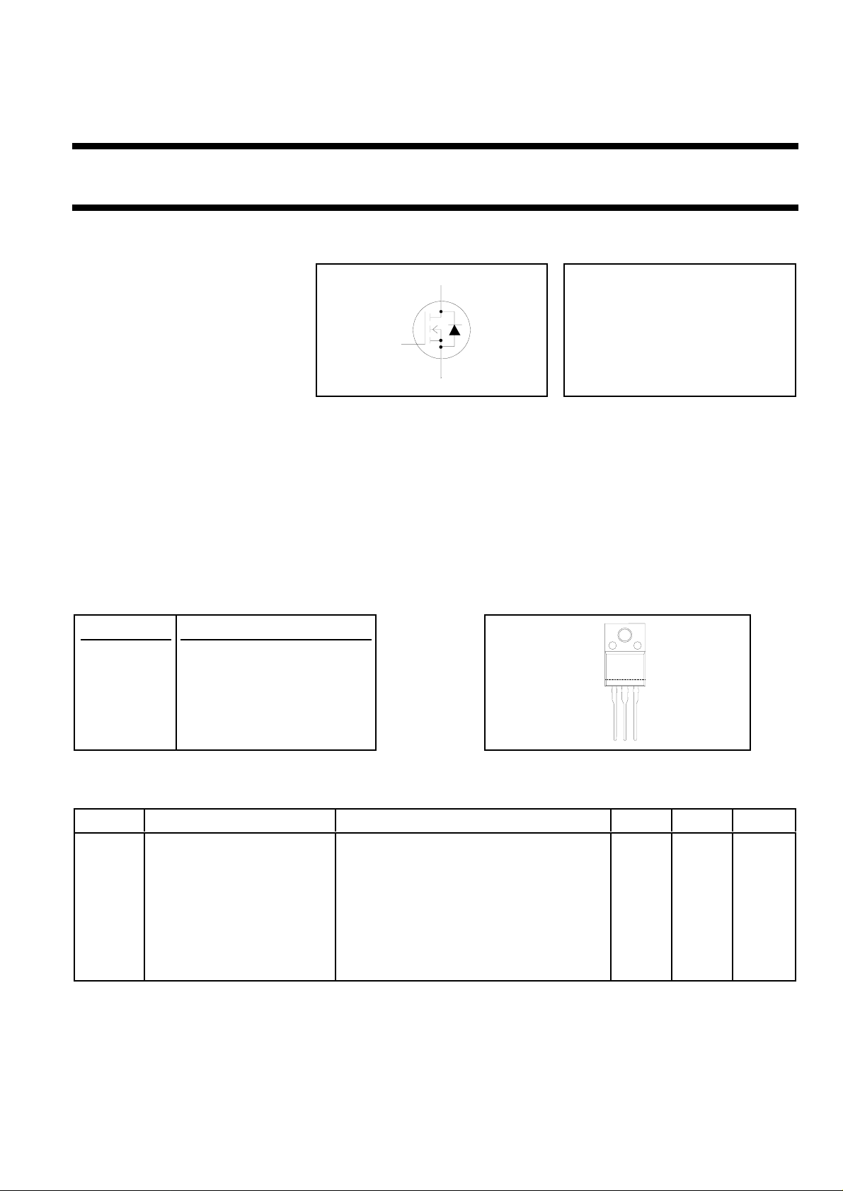
N-channel TrenchMOS transistor PHX23NQ10T
FEATURES SYMBOL QUICK REFERENCE DATA
• ’Trench’ technology
• Low on-state resistance V
d
= 100 V
DSS
• Fast switching
ID = 13 A
g
R
s
DS(ON)
≤ 70 mΩ
GENERAL DESCRIPTION
N-channel enhancement mode field-effect power transistor in a plastic full pack envelope using ’trench’ technology.
Applications:-
• d.c. to d.c. converters
• switched mode power supplies
• T.V. and computer monitor power supplies
The PHX23NQ10T is supplied in the SOT186A (FPAK) conventional leaded package.
PINNING SOT186A (FPAK)
PIN DESCRIPTION
1 gate
2 drain
case
3 source
case isolated
123
LIMITING VALUES
Limiting values in accordance with the Absolute Maximum System (IEC 134)
SYMBOL PARAMETER CONDITIONS MIN. MAX. UNIT
V
DSS
V
DGR
V
GS
I
D
I
DM
P
D
Tj, T
Drain-source voltage Tj = 25 ˚C to 150˚C - 100 V
Drain-gate voltage Tj = 25 ˚C to 150˚C; RGS = 20 kΩ - 100 V
Gate-source voltage - ± 20 V
Continuous drain current Tmb = 25 ˚C; VGS = 10 V - 13 A
Tmb = 100 ˚C; VGS = 10 V - 8 A
Pulsed drain current Tmb = 25 ˚C - 52 A
Total power dissipation Tmb = 25 ˚C - 27 W
Operating junction and - 55 150 ˚C
stg
storage temperature
September 1999 1 Rev 1.000

Philips Semiconductors Product specification
N-channel TrenchMOS transistor PHX23NQ10T
AVALANCHE ENERGY LIMITING VALUES
Limiting values in accordance with the Absolute Maximum System (IEC 134)
SYMBOL PARAMETER CONDITIONS MIN. MAX. UNIT
E
AS
I
AS
THERMAL RESISTANCES
SYMBOL PARAMETER CONDITIONS MIN. TYP. MAX. UNIT
R
th j-mb
R
th j-a
Non-repetitive avalanche Unclamped inductive load, IAS = 14 A; - 93 mJ
energy tp = 100 µs; Tj prior to avalanche = 25˚C;
VDD ≤ 25 V; RGS = 50 Ω; VGS = 10 V; refer
to fig:15
Peak non-repetitive - 23 A
avalanche current
Thermal resistance junction - - 4.6 K/W
to mounting base
Thermal resistance junction SOT186a package, in free air - 55 - K/W
to ambient
ELECTRICAL CHARACTERISTICS
Tj= 25˚C unless otherwise specified
SYMBOL PARAMETER CONDITIONS MIN. TYP. MAX. UNIT
V
(BR)DSS
V
GS(TO)
R
DS(ON)
I
GSS
I
DSS
Q
g(tot)
Q
gs
Q
gd
t
d on
t
r
t
d off
t
f
L
d
L
s
C
iss
C
oss
C
rss
Drain-source breakdown VGS = 0 V; ID = 0.25 mA; 100 - - V
voltage Tj = -55˚C 89 - - V
Gate threshold voltage VDS = VGS; ID = 1 mA 2 3 4 V
Tj = 150˚C 1.25 - - V
Tj = -55˚C - - 6 V
Drain-source on-state VGS = 10 V; ID = 13 A - 49 70 mΩ
resistance Tj = 150˚C - 115 163 mΩ
Gate source leakage current VGS = ± 10 V; VDS = 0 V - 10 100 nA
Zero gate voltage drain VDS = 100 V; VGS = 0 V - 0.05 10 µA
current Tj = 150˚C - - 500 µA
Total gate charge ID = 23 A; V
= 80 V; VGS = 10 V - 22 - nC
DD
Gate-source charge - 5 - nC
Gate-drain (Miller) charge - 10 - nC
Turn-on delay time VDD = 50 V; RD = 2.2 Ω;-8-ns
Turn-on rise time VGS = 10 V; RG = 5.6 Ω -39-ns
Turn-off delay time Resistive load - 26 - ns
Turn-off fall time - 24 - ns
Internal drain inductance Measured from drain lead to centre of die - 4.5 - nH
Internal source inductance Measured from source lead to source - 7.5 - nH
bond pad
Input capacitance VGS = 0 V; VDS = 25 V; f = 1 MHz - 890 1187 pF
Output capacitance - 139 167 pF
Feedback capacitance - 83 109 pF
September 1999 2 Rev 1.000

Philips Semiconductors Product specification
N-channel TrenchMOS transistor PHX23NQ10T
REVERSE DIODE LIMITING VALUES AND CHARACTERISTICS
Tj = 25˚C unless otherwise specified
SYMBOL PARAMETER CONDITIONS MIN. TYP. MAX. UNIT
I
S
I
SM
V
SD
t
rr
Q
rr
ISOLATION LIMITING VALUE & CHARACTERISTIC
Ths = 25 ˚C unless otherwise specified
SYMBOL PARAMETER CONDITIONS MIN. TYP. MAX. UNIT
V
isol
C
isol
Continuous source current - - 13 A
(body diode)
Pulsed source current (body - - 92 A
diode)
Diode forward voltage IF = 11 A; VGS = 0 V - 0.9 1.2 V
Reverse recovery time IF = 11 A; -dIF/dt = 100 A/µs; - 64 - ns
Reverse recovery charge VGS = 0 V; VR = 25 V - 120 - nC
R.M.S. isolation voltage from all f = 50-60 Hz; sinusoidal - 2500 V
three terminals to external waveform;
heatsink R.H. ≤ 65% ; clean and dustfree
Capacitance from T2 to external f = 1 MHz - 10 - pF
heatsink
September 1999 3 Rev 1.000
 Loading...