

Philips PHF14NQ20T, PHX14NQ20T Datasheet
Philips Semiconductors Product specification
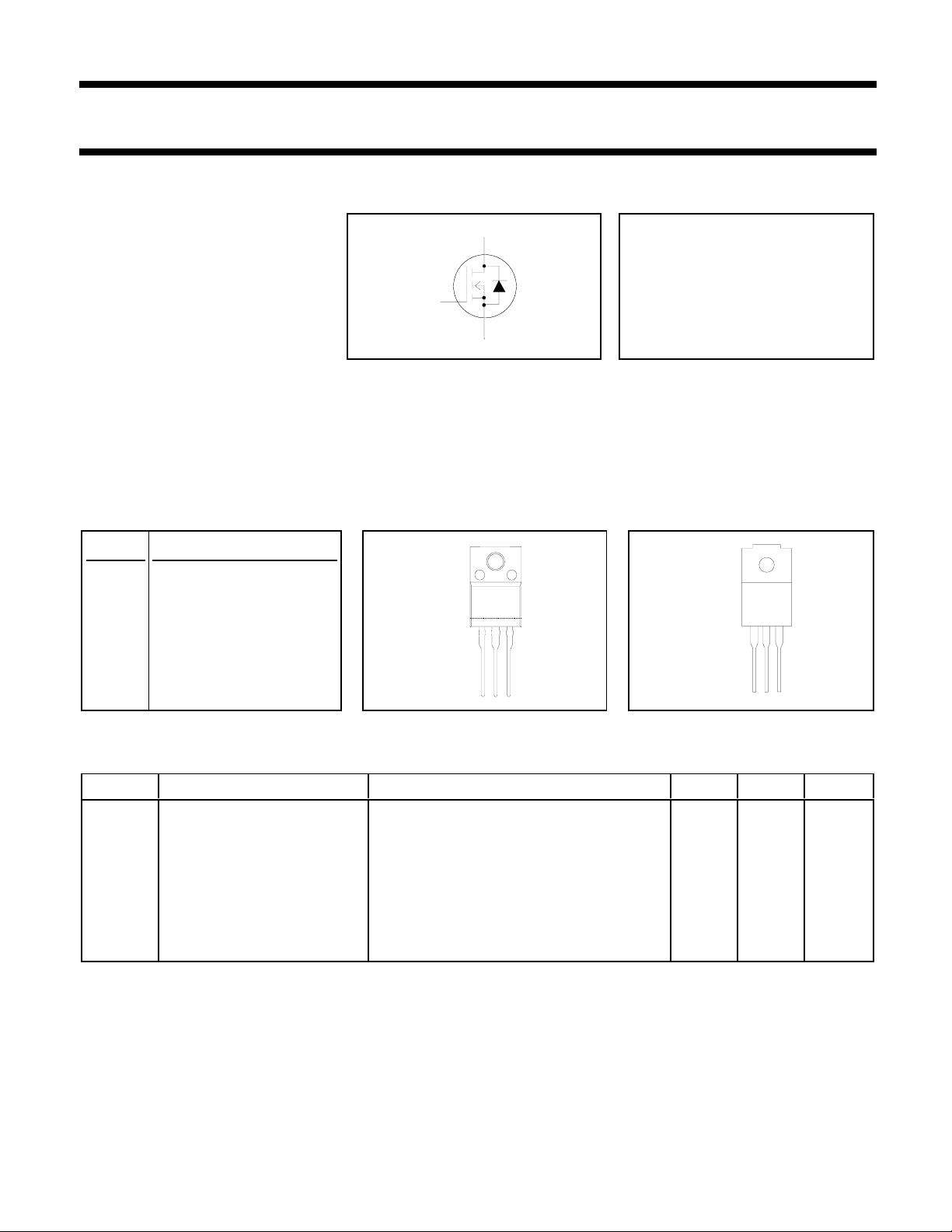
N-channel TrenchMOS transistor PHX14NQ20T , PHF14NQ20T
FEATURES SYMBOL QUICK REFERENCE DATA
• ’Trench’ technology
• Low on-state resistance V
d
= 200 V
DSS
• Fast switching
ID = 7.6 A
g
R
s
DS(ON)
≤ 230 mΩ
GENERAL DESCRIPTION
N-channel enhancement mode field-effect power transistor in a plastic full pack envelope using ’trench’ technology.
Thedevicehas very low on-state resistance. Itisintended for use in dctodc converters and general purpose switching
applications.
The PHX14NQ20T is supplied in the SOT186A (FPAK) conventional leaded package.
PINNING SOT186A (FPAK) SOT186 (FPAK)
PIN DESCRIPTION
1 gate
case
2 drain
3 source
case
case isolated
123
123
LIMITING VALUES
Limiting values in accordance with the Absolute Maximum System (IEC 134)
SYMBOL PARAMETER CONDITIONS MIN. MAX. UNIT
V
DSS
V
DGR
V
GS
I
D
I
DM
P
D
Tj, T
Drain-source voltage Tj = 25 ˚C to 150˚C - 200 V
Drain-gate voltage Tj = 25 ˚C to 150˚C; RGS = 20 kΩ - 200 V
Gate-source voltage - ± 20 V
Continuous drain current Ths = 25 ˚C; VGS = 10 V - 7.6 A
Ths = 100 ˚C; VGS = 10 V - 4.8 A
Pulsed drain current Ths = 25 ˚C - 30 A
Total power dissipation Ths = 25 ˚C - 30 W
Operating junction and - 55 150 ˚C
stg
storage temperature
November 2000 1 Rev 1.100
Philips Semiconductors Product specification
N-channel TrenchMOS transistor PHX14NQ20T , PHF14NQ20T
AVALANCHE ENERGY LIMITING VALUES
Limiting values in accordance with the Absolute Maximum System (IEC 134)
SYMBOL PARAMETER CONDITIONS MIN. MAX. UNIT
E
AS
I
AS
THERMAL RESISTANCES
SYMBOL PARAMETER CONDITIONS MIN. TYP. MAX. UNIT
R
th j-hs
R
th j-a
Non-repetitive avalanche Unclamped inductive load, IAS = 14 A; - 70 mJ
energy tp = 38 µs; Tj prior to avalanche = 25˚C;
VDD ≤ 25 V; RGS = 50 Ω; VGS = 10 V; refer
to fig 15
Peak non-repetitive - 14 A
avalanche current
Thermal resistance junction - - 4.17 K/W
to mounting base
Thermal resistance junction SOT186A package, in free air - 55 - K/W
to ambient
ELECTRICAL CHARACTERISTICS
Tj= 25˚C unless otherwise specified
SYMBOL PARAMETER CONDITIONS MIN. TYP. MAX. UNIT
V
(BR)DSS
V
GS(TO)
R
DS(ON)
g
fs
I
GSS
I
DSS
Q
g(tot)
Q
gs
Q
gd
t
d on
t
r
t
d off
t
f
L
d
L
s
C
iss
C
oss
C
rss
Drain-source breakdown VGS = 0 V; ID = 0.25 mA; 200 - - V
voltage Tj = -55˚C 178 - - V
Gate threshold voltage VDS = VGS; ID = 1 mA 2 3 4 V
Tj = 150˚C 1 - - V
Tj = -55˚C - - 6 V
Drain-source on-state VGS = 10 V; ID = 7 A - 150 230 mΩ
resistance VGS = 10 V; ID = 7 A; Tj = 150˚C - - 540 mΩ
Forward transconductance VDS = 25 V; ID = 7 A 6 12.1 - S
Gate source leakage current VGS = ± 10 V; VDS = 0 V - 10 100 nA
Zero gate voltage drain VDS = 200 V; VGS = 0 V - 0.05 10 µA
current Tj = 150˚C - - 500 µA
Total gate charge ID = 14 A; V
= 160 V; VGS = 10 V - 38 - nC
DD
Gate-source charge - 4 - nC
Gate-drain (Miller) charge - 13.3 - nC
Turn-on delay time VDD = 100 V; RD = 10 Ω; - 25 - ns
Turn-on rise time VGS = 10 V; RG = 5.6 Ω -40-ns
Turn-off delay time Resistive load - 83 - ns
Turn-off fall time - 31 - ns
Internal drain inductance Measured from drain lead to centre of die - 4.5 - nH
Internal source inductance Measured from source lead to source - 7.5 - nH
bond pad
Input capacitance VGS = 0 V; VDS = 25 V; f = 1 MHz - 1500 - pF
Output capacitance - 128 - pF
Feedback capacitance - 60 - pF
November 2000 2 Rev 1.100

Philips Semiconductors Product specification
N-channel TrenchMOS transistor PHX14NQ20T , PHF14NQ20T
REVERSE DIODE LIMITING VALUES AND CHARACTERISTICS
Tj = 25˚C unless otherwise specified
SYMBOL PARAMETER CONDITIONS MIN. TYP. MAX. UNIT
I
S
I
SM
V
SD
t
rr
Q
rr
ISOLATION LIMITING VALUE & CHARACTERISTIC
Ths = 25 ˚C unless otherwise specified
SYMBOL PARAMETER CONDITIONS MIN. TYP. MAX. UNIT
V
isol
V
isol
C
isol
Continuous source current - - 14 A
(body diode)
Pulsed source current (body - - 56 A
diode)
Diode forward voltage IF = 14 A; VGS = 0 V - 1.0 1.5 V
Reverse recovery time IF = 14 A; -dIF/dt = 100 A/µs; - 135 - ns
Reverse recovery charge VGS = 0 V; VR = 30 V - 690 - nC
R.M.S. isolation voltage from all SOT186A package; f = 50-60 Hz; - 2500 V
three terminals to external sinusoidal waveform; R.H. ≤ 65%;
heatsink clean and dustfree
Repetitive peak voltage from all SOT186 package; R.H. ≤ 65%; - 1500 V
three terminals to external clean and dustfree
heatsink
Capacitance from pin 2 to f = 1 MHz - 10 - pF
external heatsink
November 2000 3 Rev 1.100
 Loading...