

Philips PDZ12B, PDZ13B, PDZ15B, PDZ30B, PDZ27B Datasheet
...
DISCRETE SEMICONDUCTORS
DATA SH EET
ook, halfpage
M3D049
PDZ-B series
Voltage regulator diodes
Product specification
Supersedes data of 1998 Jan 09
1998 Apr 23
Philips Semiconductors Product specification
Voltage regulator diodes PDZ-B series
FEATURES
• Total power dissipation:
max. 400 mW
• Small plastic package suitable for
surface mounted design
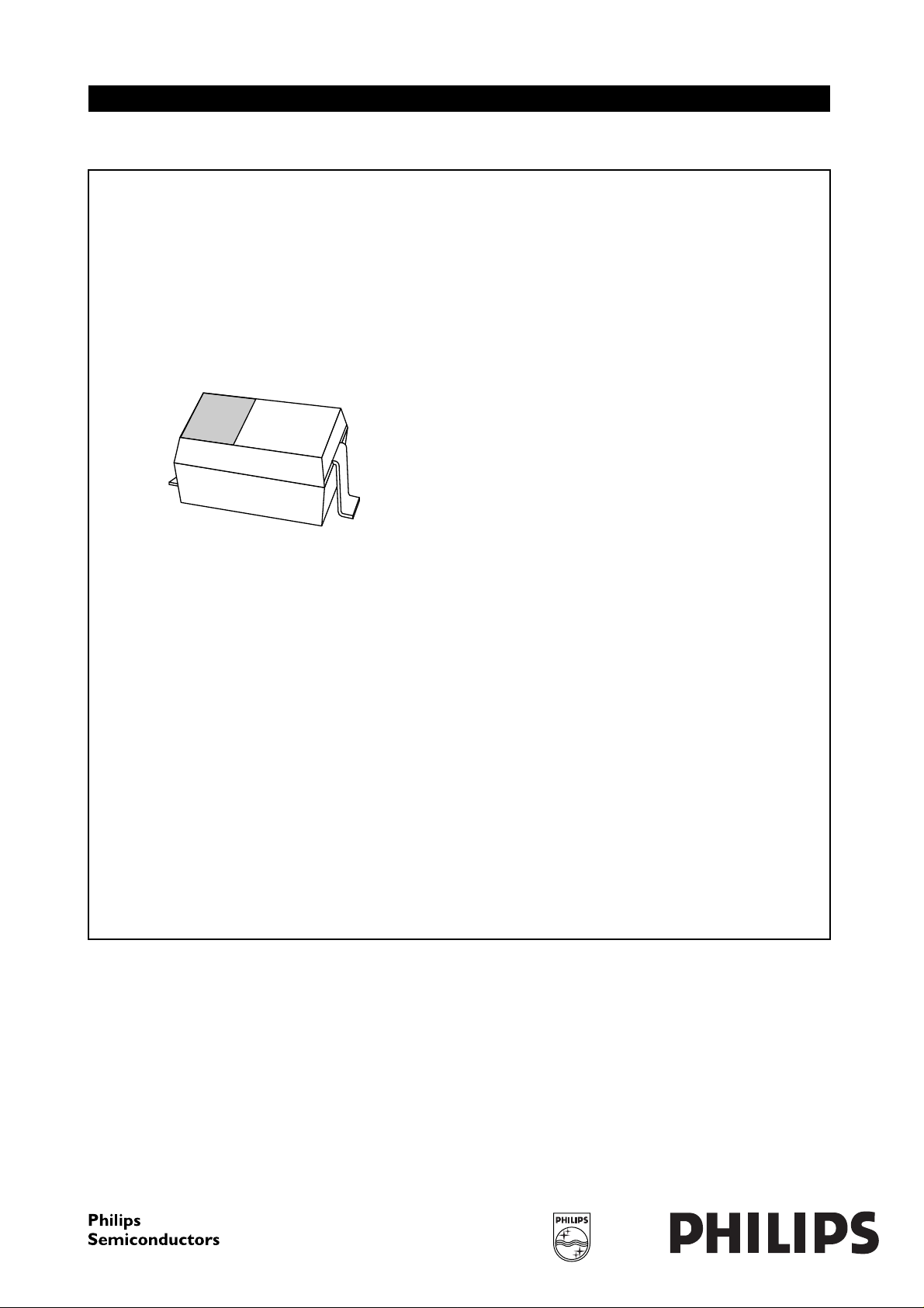
DESCRIPTION
Low-power general purpose voltage
regulator diodes in a small plastic
SMD SOD323 package.
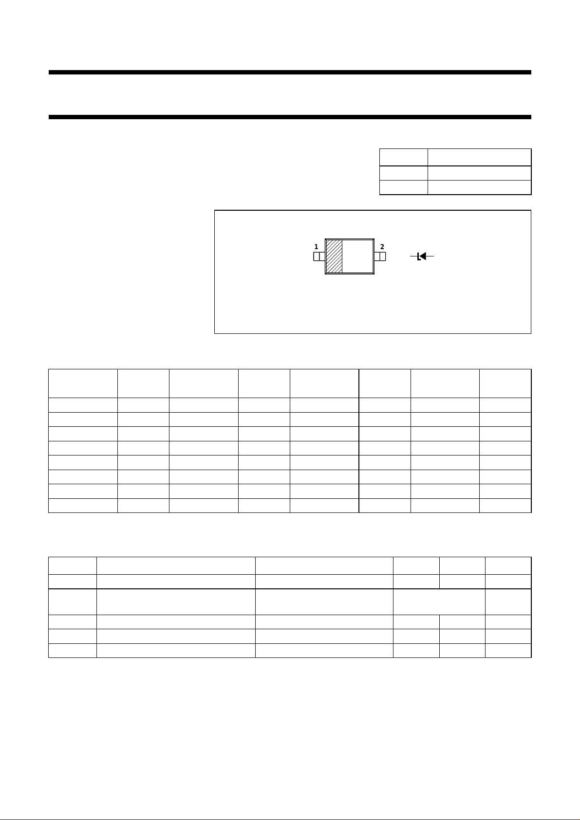
PINNING
PIN DESCRIPTION
1 cathode
2 anode
• Wide variety of voltage ranges:
nom. 2.4 to 36 V (E24 range).
APPLICATIONS
handbook, halfpage
12
• General voltage regulation.
Top view
MAM387
Fig.1 Simplified outline (SOD323) and symbol.
MARKING
TYPE
NUMBER
MARKING
CODE
TYPE
NUMBER
MARKING
CODE
TYPE
NUMBER
MARKING
CODE
TYPE
NUMBER
PDZ2.4B Z0 PDZ5.1B Z8 PDZ11B ZG PDZ24B ZQ
PDZ2.7B Z1 PDZ5.6B Z9 PDZ12B ZH PDZ27B ZR
PDZ3.0B Z2 PDZ6.2B ZA PDZ13B ZJ PDZ30B ZS
PDZ3.3B Z3 PDZ6.8B ZB PDZ15B ZK PDZ33B ZT
PDZ3.6B Z4 PDZ7.5B ZC PDZ16B ZL PDZ36B ZU
PDZ3.9B Z5 PDZ8.2B ZD PDZ18B ZM
PDZ4.3B Z6 PDZ9.1B ZE PDZ20B ZN
PDZ4.7B Z7 PDZ10B ZF PDZ22B ZP
MARKING
CODE
LIMITING VALUES
In accordance with the Absolute Maximum Rating System (IEC 134).
SYMBOL PARAMETER CONDITIONS MIN. MAX. UNIT
I
F
I
ZSM
P
T
T
tot
stg
j
continuous forward current − 200 mA
non-repetitive peak reverse current tp= 100 µs; square wave;
T
=25°C prior to surge
amb
total power dissipation T
=25°C; note 1; see Fig.2 − 400 mW
amb
see Table 2
storage temperature −65 +150 °C
junction temperature − 150 °C
Note
1. Device mounted on a printed-circuit board measuring 11 × 25 × 1.6 mm.
1998 Apr 23 2

Philips Semiconductors Product specification
Voltage regulator diodes PDZ-B series
THERMAL CHARACTERISTICS
SYMBOL PARAMETER CONDITIONS VALUE UNIT
R
th j-s
R
th j-a
Note
1. Device mounted on a printed-circuit board measuring 11 × 25 × 1.6 mm.
ELECTRICAL CHARACTERISTICS
Table 1 Total series
T
=25°C unless otherwise specified.
j
SYMBOL PARAMETER CONDITIONS MAX. UNIT
V
F
I
R
thermal resistance from junction to soldering point 130 K/W
thermal resistance from junction to ambient note 1 340 K/W
forward voltage IF= 10 mA; see Fig.3 0.9 V
I
= 100 mA; see Fig.3 1.1 V
F
reverse current
PDZ2.4B V
PDZ2.7B V
PDZ3.0B V
PDZ3.3B V
PDZ3.6B V
PDZ3.9B V
PDZ4.3B V
PDZ4.7B V
PDZ5.1B V
PDZ5.6B V
PDZ6.2B V
PDZ6.8B V
PDZ7.5B V
PDZ8.2B V
PDZ9.1B V
PDZ10B V
PDZ11B V
PDZ12B V
PDZ13B V
PDZ15B V
PDZ16B V
PDZ18B V
PDZ20B V
PDZ22B V
PDZ24B V
PDZ27B V
PDZ30B V
PDZ33B V
PDZ36B V
=1V 50 µA
R
=1V 20 µA
R
=1V 10 µA
R
=1V 5 µA
R
=1V 5 µA
R
=1V 3 µA
R
=1V 3 µA
R
=1V 2 µA
R
= 1.5 V 2 µA
R
= 2.5 V 1 µA
R
= 3 V 500 nA
R
= 3.5 V 500 nA
R
= 4 V 500 nA
R
= 5 V 500 nA
R
= 6 V 500 nA
R
= 7 V 100 nA
R
= 8 V 100 nA
R
= 9 V 100 nA
R
= 10 V 100 nA
R
= 11 V 50 nA
R
= 12 V 50 nA
R
= 13 V 50 nA
R
= 15 V 50 nA
R
= 17 V 50 nA
R
= 19 V 50 nA
R
= 21 V 50 nA
R
= 23 V 50 nA
R
= 25 V 50 nA
R
= 27 V 50 nA
R
1998 Apr 23 3
 Loading...