

Page 1

PDTA144V series
PNP resistor-equipped transistors; R1 = 47 kΩ, R2 = 10 kΩ
Rev. 04 — 3 September 2009 Product data sheet
1. Product profile
1.1 General description
PNP resistor-equipped transistors.
Table 1. Product overview
Type number Package NPN complement
PDTA144VE SOT416 SC-75 PDTC144VE
PDTA144VK SOT346 SC-59A PDTC144VK
PDTA144VM SOT883 SC-101 PDTC144VM
PDTA144VS
PDTA144VT SOT23 - PDTC144VT
PDTA144VU SOT323 SC-70 PDTC144VU
NXP JEITA
[1]
SOT54 SC-43A PDTC144VS
[1] Also available in SOT54A and SOT54 variant packages (seeSection 2)
1.2 Features
n Built-in bias resistors n Reduces component count
n Simplifies circuit design n Reduces pick and place costs
1.3 Applications
n General purpose switching and
amplification
n Inverter and interface circuits
n Circuit drivers
1.4 Quick reference data
Table 2. Quick reference data
Symbol Parameter Conditions Min Typ Max Unit
V
CEO
I
O
R1 bias resistor 1 (input) 33 47 61 kΩ
R2/R1 bias resistor ratio 0.17 0.21 0.26
collector-emitter voltage open base - - −50 V
output current (DC) - - −100 mA
Page 2
NXP Semiconductors
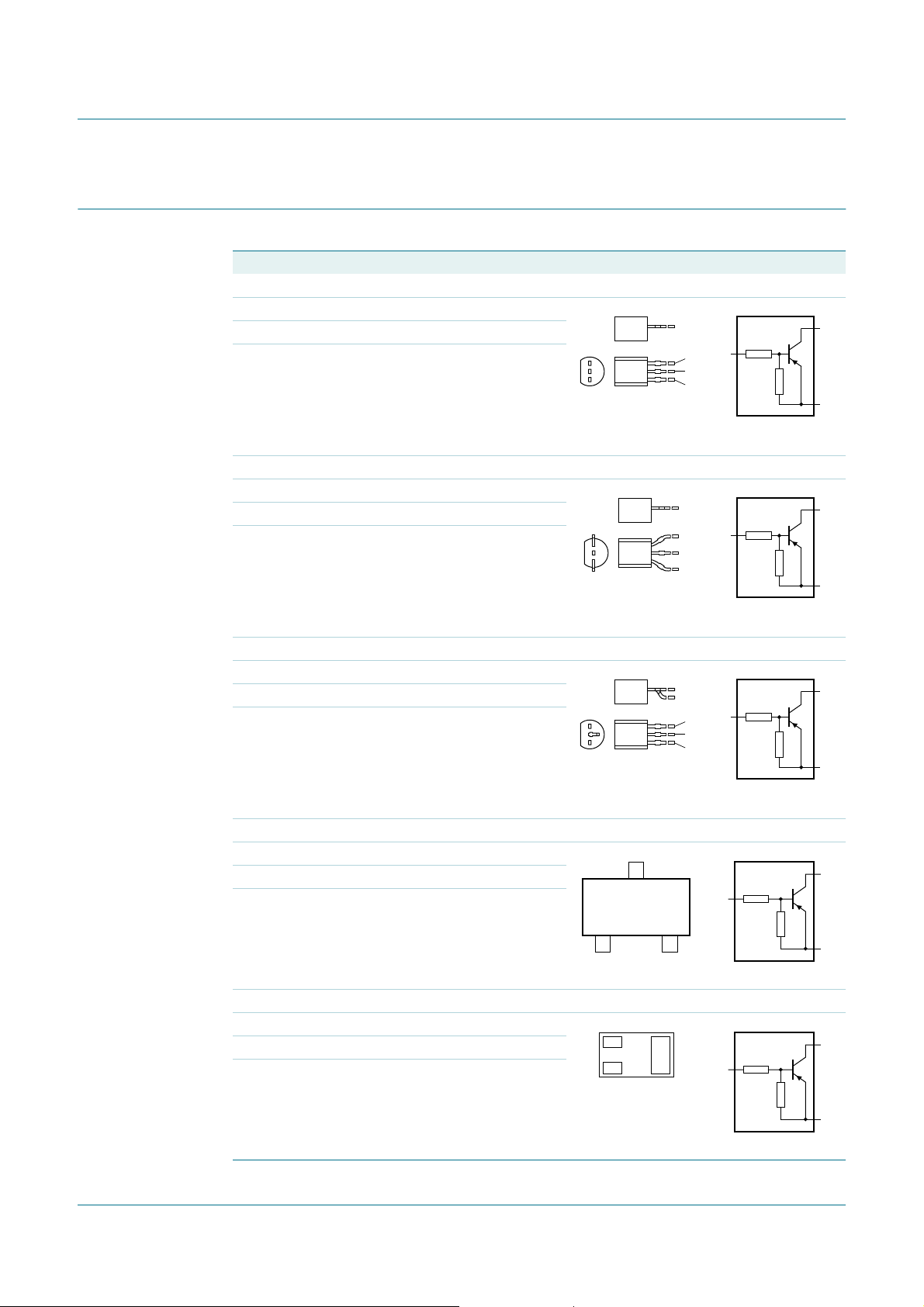
2. Pinning information
Table 3. Pinning
Pin Description Simplified outline Symbol
SOT54
1 input (base)
2 output (collector)
3 GND (emitter)
SOT54A
1 input (base)
2 output (collector)
3 GND (emitter)
PDTA144V series
PNP resistor-equipped transistors; R1 = 47 kΩ, R2 = 10 kΩ
2
3
2
3
001aab347
001aab348
R1
1
1
2
3
1
2
3
R2
006aaa148
R1
1
R2
006aaa148
SOT54 variant
1 input (base)
2 output (collector)
3 GND (emitter)
SOT23, SOT323, SOT346, SOT416
1 input (base)
2 GND (emitter)
3 output (collector)
SOT883
1 input (base)
2 GND (emitter)
3 output (collector)
1
2
3
001aab447
3
12
006aaa144
1
2
Transparent
top view
3
R1
1
R2
006aaa148
R1
1
R1
1
2
3
3
R2
2
sym003
3
R2
2
sym003
PDTA144V_SER_4 © NXP B.V. 2009. All rights reserved.
Product data sheet Rev. 04 — 3 September 2009 2 of 18
Page 3

NXP Semiconductors
3. Ordering information
Table 4. Ordering information
Type number Package
PDTA144VE SC-75 plastic surface mounted package; 3 leads SOT416
PDTA144VK SC-59A plastic surface mounted package; 3 leads SOT346
PDTA144VM SC-101 leadless ultra small plastic package; 3 solder lands;
PDTA144VS
PDTA144VT - plastic surface mounted package; 3 leads SOT23
PDTA144VU SC-70 plastic surface mounted package; 3 leads SOT323
[1] Also available in SOT54A and SOT54 variant packages (seeSection 2 and Section 9).
[1]
4. Marking
PDTA144V series
PNP resistor-equipped transistors; R1 = 47 kΩ, R2 = 10 kΩ
Name Description Version
SOT883
body 1.0 × 0.6 × 0.5 mm
SC-43A plastic single-ended leaded (through hole) package;
3 leads
SOT54
Table 5. Marking codes
Type number Marking code
PDTA144VE 13
PDTA144VK 12
PDTA144VM E9
PDTA144VS TA144V
PDTA144VT *AG
PDTA144VU *12
[1] * = -: made in Hong Kong
* = p: made in Hong Kong
* = t: made in Malaysia
* = W: made in China
[1]
PDTA144V_SER_4 © NXP B.V. 2009. All rights reserved.
Product data sheet Rev. 04 — 3 September 2009 3 of 18
Page 4

NXP Semiconductors
5. Limiting values
Table 6. Limiting values
In accordance with the Absolute Maximum Rating System (IEC 60134).
Symbol Parameter Conditions Min Max Unit
V
CBO
V
CEO
V
EBO
V
I
I
O
I
CM
P
tot
T
stg
T
j
T
amb
[1] Refer to standard mounting conditions.
[2] Reflow soldering is the only recommended soldering method.
[3] Refer to SOT883 standard mounting conditions; FR4 printed-circuit board with 60 µm copper strip line.
PDTA144V series
PNP resistor-equipped transistors; R1 = 47 kΩ, R2 = 10 kΩ
collector-base voltage open emitter - −50 V
collector-emitter voltage open base - −50 V
emitter-base voltage open collector - −15 V
input voltage
positive - +15 V
negative - −40 V
output current (DC) - −100 mA
peak collector current - −100 mA
total power dissipation T
SOT416
SOT346
SOT883
SOT54
SOT23
SOT323
storage temperature −65 +150 °C
junction temperature - 150 °C
ambient temperature −65 +150 °C
amb
≤ 25 °C
[1]
- 150 mW
[1]
- 250 mW
[2][3]
- 250 mW
[1]
- 500 mW
[1]
- 250 mW
[1]
- 200 mW
6. Thermal characteristics
Table 7. Thermal characteristics
Symbol Parameter Conditions Min Typ Max Unit
R
th(j-a)
thermal resistance from
junction to ambient
SOT416
SOT346
SOT883
SOT54
SOT23
SOT323
[1] Refer to standard mounting conditions.
[2] Reflow soldering is the only recommended soldering method.
[3] Refer to SOT883 standard mounting conditions; FR4 printed-circuit board with 60 µm copper strip line.
PDTA144V_SER_4 © NXP B.V. 2009. All rights reserved.
Product data sheet Rev. 04 — 3 September 2009 4 of 18
in free air
[1]
- - 833 K/W
[1]
- - 500 K/W
[2][3]
- - 500 K/W
[1]
- - 250 K/W
[1]
- - 500 K/W
[1]
- - 625 K/W
Page 5

NXP Semiconductors
PDTA144V series
PNP resistor-equipped transistors; R1 = 47 kΩ, R2 = 10 kΩ
7. Characteristics
Table 8. Characteristics
T
= 25°C unless otherwise specified
amb
Symbol Parameter Conditions Min Typ Max Unit
I
CBO
collector-base cut-off
current
I
CEO
collector-emitter
cut-off current
I
EBO
emitter-base cut-off
current
h
V
FE
CEsat
DC current gain VCE = −5 V; IC = −5 mA 40 - -
collector-emitter
saturation voltage
V
I(off)
V
I(on)
off-state input voltage VCE = −5 V; IC = −100 µA-−3.1 −1V
on-state input voltage VCE = −300 mV; IC = −2mA −6 −3.8 - V
R1 bias resistor 1 (input) 33 47 61 kΩ
R2/R1 bias resistor ratio 0.17 0.21 0.26
C
c
collector capacitance VCB = −10 V; IE = ie = 0 A;
VCB = −50 V; IE = 0 A - - −100 nA
VCE = −30 V; IB = 0 A - - −1 µA
= −30 V; IB = 0 A;
V
CE
T
= 150 °C
j
--−50 µA
VEB = −5 V; IC = 0 A - - −150 µA
IC = −10 mA; IB = −0.5 mA - - −150 mV
--2pF
f=1MHz
PDTA144V_SER_4 © NXP B.V. 2009. All rights reserved.
Product data sheet Rev. 04 — 3 September 2009 5 of 18
Page 6
NXP Semiconductors
PDTA144V series
PNP resistor-equipped transistors; R1 = 47 kΩ, R2 = 10 kΩ
3
10
h
FE
2
10
10
1
−1
−10
006aaa111
(1)(2)
(3)
2
−10−1
IC (mA)
−10
VCE = −5 V
(1) T
(2) T
(3) T
= 100 °C
amb
= 25 °C
amb
= −40 °C
amb
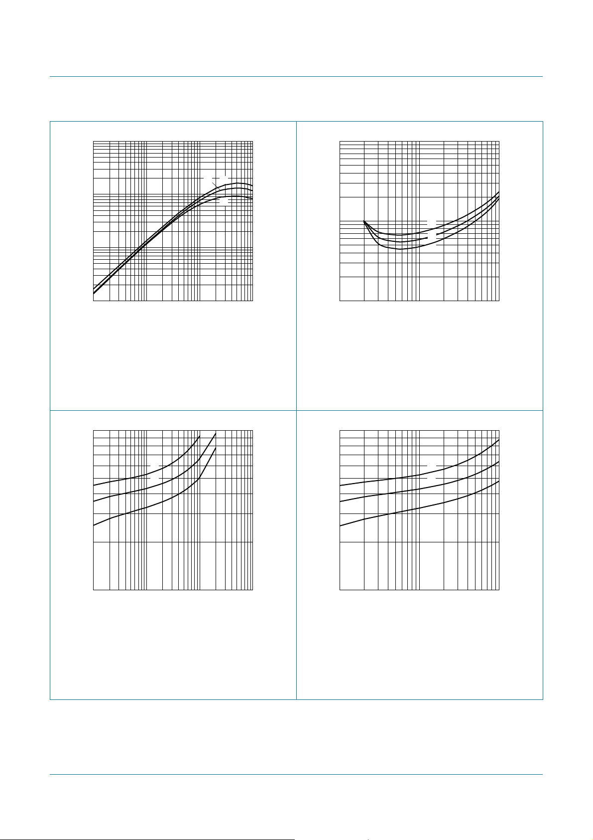
Fig 1. DC current gain as a function of collector
current; typical values
−1
V
CEsat
(V)
−1
−10
−2
−10
−1 −10
(1)
(2)
(3)
−10
006aaa112
IC (mA)
IC/IB = 20
(1) T
(2) T
(3) T
= 100 °C
amb
= 25 °C
amb
= −40 °C
amb
Fig 2. Collector-emitter saturation voltage as a
function of collector current; typical values
2
−10
V
I(on)
(V)
−1
−1
−10
(1)
(2)
(3)
006aaa113
−10−1
IC (mA)
−10
VCE = −0.3 V
(1) T
(2) T
(3) T
= −40 °C
amb
= 25 °C
amb
= 100 °C
amb
Fig 3. On-state input voltage as a function of
collector current; typical values
IC (mA)
006aaa114
−10−1
−10
V
I(off)
(V)
2
−1
−10
−1
(1)
(2)
(3)
VCE = −5 V
(1) T
(2) T
(3) T
= −40 °C
amb
= 25 °C
amb
= 100 °C
amb
Fig 4. Off-state input voltage as a function of
collector current; typical values
PDTA144V_SER_4 © NXP B.V. 2009. All rights reserved.
Product data sheet Rev. 04 — 3 September 2009 6 of 18
Page 7
NXP Semiconductors
PDTA144V series
PNP resistor-equipped transistors; R1 = 47 kΩ, R2 = 10 kΩ
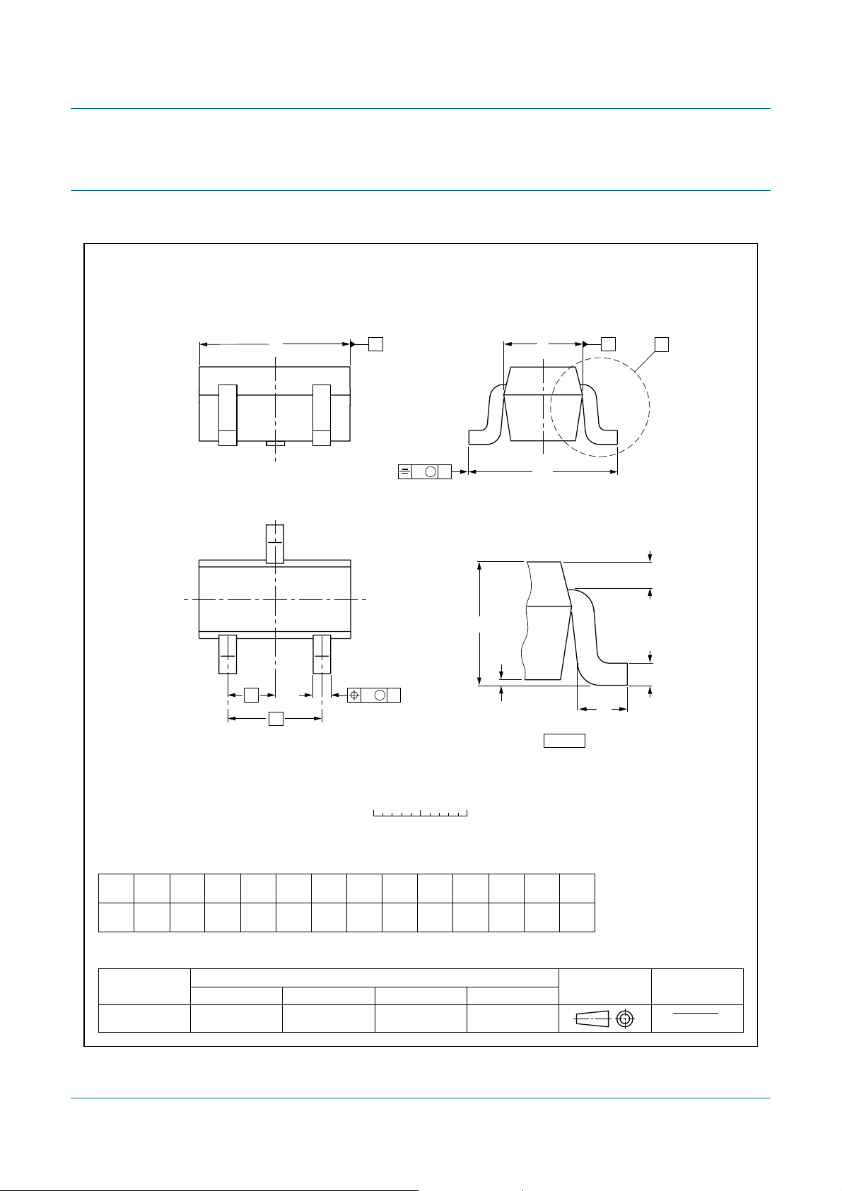
8. Package outline
Plastic surface-mounted package; 3 leads SOT416
D
v M
A
3
12
e
b
1
p
e
w M
B
E
H
E
A
A
1
detail X
AB
L
p
X
Q
c
0 0.5 1 mm
scale
DIMENSIONS (mm are the original dimensions)
A
1
UNIT
A
0.95
mm
0.60
OUTLINE
VERSION
SOT416 SC-75
max
0.1
b
cD
p
0.30
0.25
0.10
1.8
1.4
0.15
IEC JEDEC JEITA
e
E
0.9
1
0.7
REFERENCES
0.5
e
H
L
Qw
1
1.75
1.45
p
E
0.45
0.23
0.15
0.13
v
0.2
0.2
EUROPEAN
PROJECTION
ISSUE DATE
04-11-04
06-03-16
Fig 5. Package outline SOT416 (SC-75)
PDTA144V_SER_4 © NXP B.V. 2009. All rights reserved.
Product data sheet Rev. 04 — 3 September 2009 7 of 18
Page 8
NXP Semiconductors
PDTA144V series
PNP resistor-equipped transistors; R1 = 47 kΩ, R2 = 10 kΩ
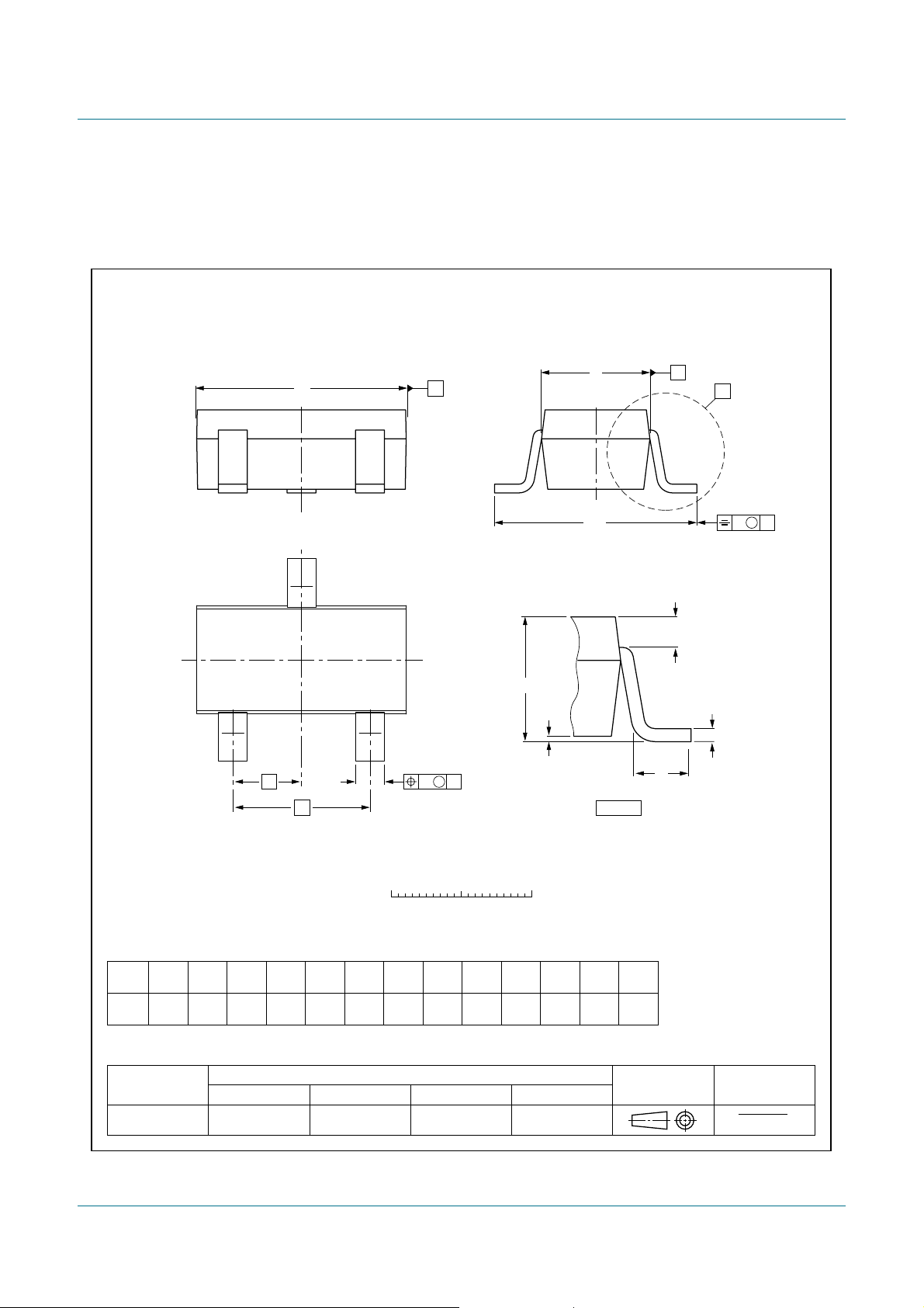
Plastic surface-mounted package; 3 leads SOT346
D
B
3
A
A
1
12
e
1
b
p
e
w M
B
E
H
E
detail X
A
X
v M
A
Q
c
L
p
0 1 2 mm
scale
DIMENSIONS (mm are the original dimensions)
1.3
1.0
A
b
A
1
0.1
0.013
cD
p
0.50
0.26
0.35
0.10
IEC JEDEC JEITA
3.1
2.7
E
1.7
1.3
REFERENCES
1.9
e
H
L
0.6
0.2
Qwv
p
0.33
0.2
0.23
0.2
EUROPEAN
PROJECTION
ISSUE DATE
04-11-11
06-03-16
e
1
E
3.0
0.95
2.5
UNIT
mm
OUTLINE
VERSION
SOT346 TO-236 SC-59A
Fig 6. Package outline SOT346 (SC-59A/TO-236)
PDTA144V_SER_4 © NXP B.V. 2009. All rights reserved.
Product data sheet Rev. 04 — 3 September 2009 8 of 18
Page 9
NXP Semiconductors
PDTA144V series
PNP resistor-equipped transistors; R1 = 47 kΩ, R2 = 10 kΩ
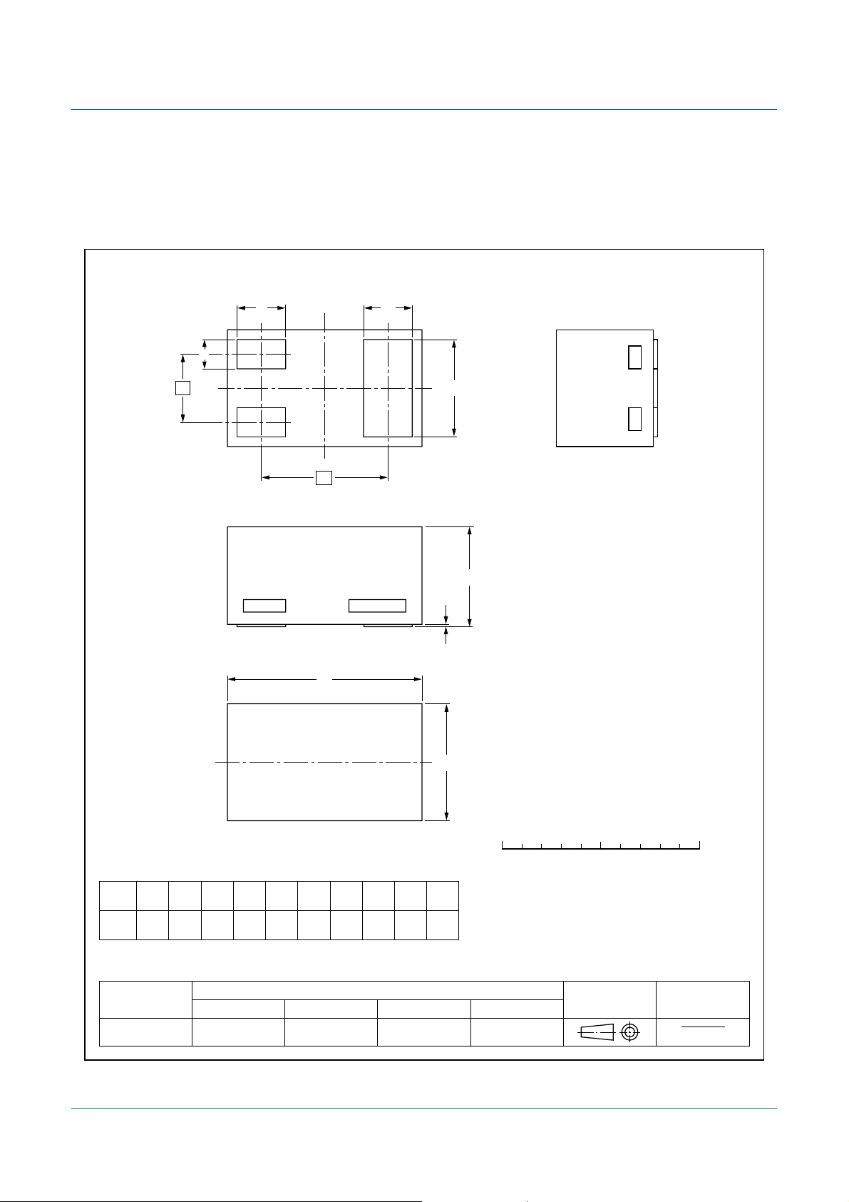
Leadless ultra small plastic package; 3 solder lands; body 1.0 x 0.6 x 0.5 mm SOT883
L
2
b
e
1
e
1
E
L
1
3
b
1
A
A
1
D
0 0.5 1 mm
scale
DIMENSIONS (mm are the original dimensions)
A
(1)
1
A
UNIT
0.50
mm
0.46
Note
1. Including plating thickness
OUTLINE
VERSION
SOT883 SC-101
max.
0.03
bb
0.20
0.12
IEC JEDEC JEITA
1
0.55
0.47
DE
0.62
1.02
0.55
0.95
e
eLL
1
0.35 0.65
REFERENCES
0.30
0.22
0.30
0.22
1
EUROPEAN
PROJECTION
ISSUE DATE
03-02-05
03-04-03
Fig 7. Package outline SOT883 (SC-101)
PDTA144V_SER_4 © NXP B.V. 2009. All rights reserved.
Product data sheet Rev. 04 — 3 September 2009 9 of 18
Page 10
NXP Semiconductors
PDTA144V series
PNP resistor-equipped transistors; R1 = 47 kΩ, R2 = 10 kΩ
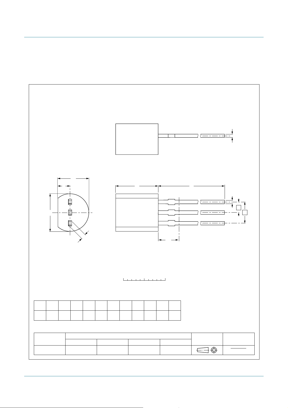
Plastic single-ended leaded (through hole) package; 3 leads SOT54
c
E
d
A L
1
D
2
3
b
1
0 2.5 5 mm
scale
DIMENSIONS (mm are the original dimensions)
UNIT
A
b
5.2
0.48
mm
5.0
Note
1. Terminal dimensions within this zone are uncontrolled to allow for flow of plastic and terminal irregularities.
OUTLINE
VERSION
SOT54 TO-92 SC-43A
0.40
0.66
0.55
c
D
d
E
4.2
3.6
e
2.54
b
1
0.45
4.8
4.4
1.7
1.4
REFERENCES
0.38
IEC JEDEC JEITA
e
1.27
1
L
14.5
12.7
L
1
(1)
L
1
max.
2.5
EUROPEAN
PROJECTION
b
e
1
e
ISSUE DATE
04-06-28
04-11-16
Fig 8. Package outline SOT54 (SC-43A/TO-92)
PDTA144V_SER_4 © NXP B.V. 2009. All rights reserved.
Product data sheet Rev. 04 — 3 September 2009 10 of 18
Page 11
NXP Semiconductors
PDTA144V series
PNP resistor-equipped transistors; R1 = 47 kΩ, R2 = 10 kΩ
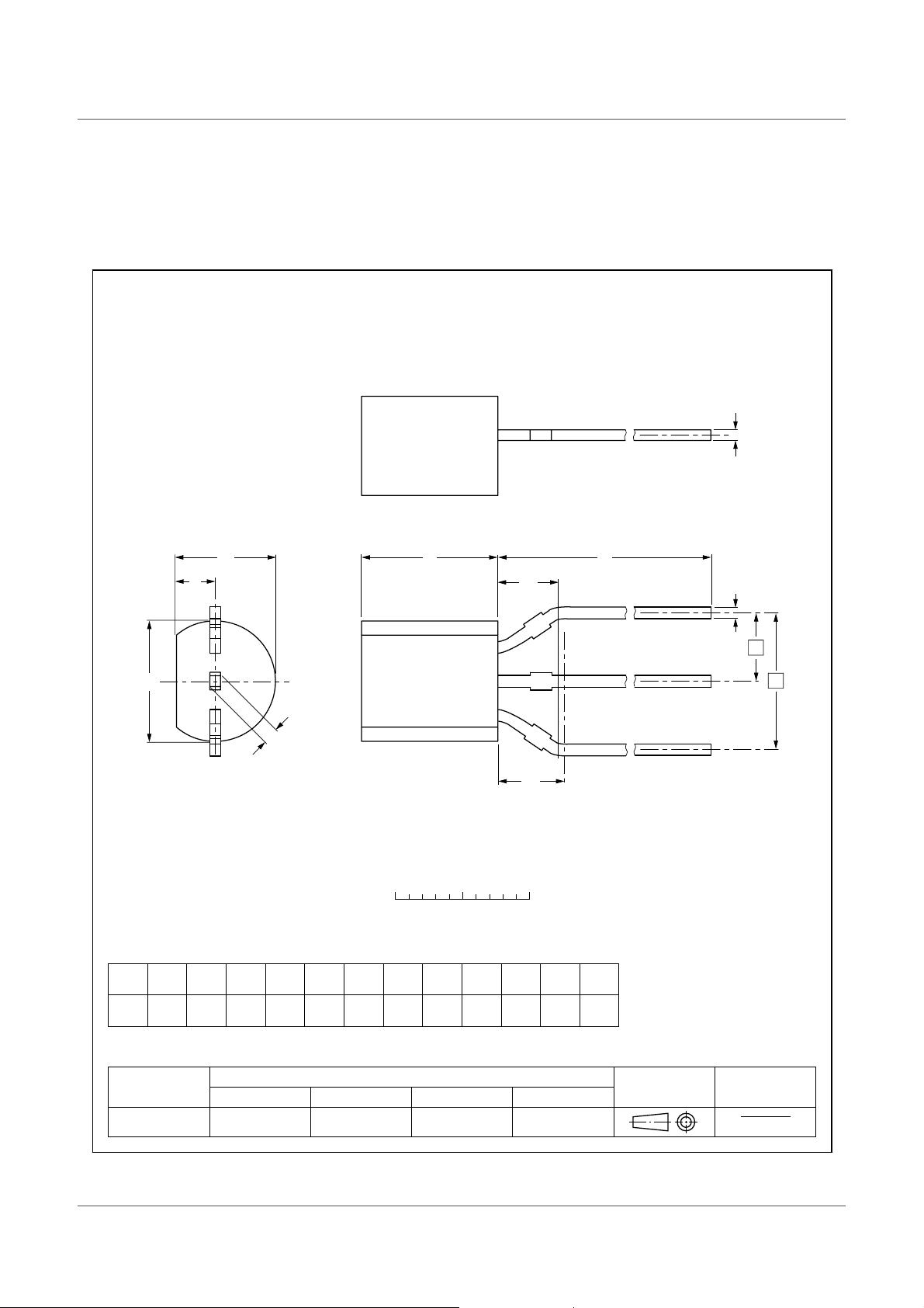
Plastic single-ended leaded (through hole) package; 3 leads (wide pitch) SOT54A
c
E
d
A
L
2
L
1
D
DIMENSIONS (mm are the original dimensions)
UNIT
A
5.2
mm
5.0
Note
1. Terminal dimensions within this zone are uncontrolled to allow for flow of plastic and terminal irregularities.
OUTLINE
VERSION
SOT54A
b
0.48
0.40
2
3
b
1
0 2.5 5 mm
b
c
D
d
1
0.66
0.45
0.38
4.8
4.4
0.55
IEC JEDEC JEITA
E
1.7
4.2
1.4
3.6
REFERENCES
e
5.08
scale
e
2.54
L
1
(1)
L
1
L
1
14.5
12.7
max.
3
L
2
3
2
EUROPEAN
PROJECTION
b
e
1
e
ISSUE DATE
97-05-13
04-06-28
Fig 9. Package outline SOT54A
PDTA144V_SER_4 © NXP B.V. 2009. All rights reserved.
Product data sheet Rev. 04 — 3 September 2009 11 of 18
Page 12
NXP Semiconductors
PDTA144V series
PNP resistor-equipped transistors; R1 = 47 kΩ, R2 = 10 kΩ
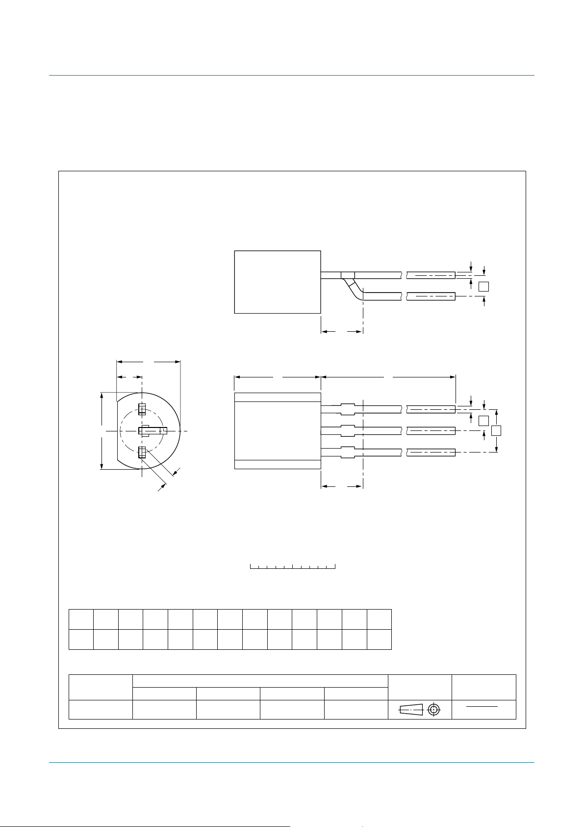
Plastic single-ended leaded (through hole) package; 3 leads (on-circle) SOT54 variant
c
e
1
L
2
E
d
A L
1
2
D
3
b
1
0 2.5 5 mm
scale
DIMENSIONS (mm are the original dimensions)
UNIT
A
5.2
mm
5.0
Note
1. Terminal dimensions within this zone are uncontrolled to allow for flow of plastic and terminal irregularities.
OUTLINE
VERSION
SOT54 variant
b
0.48
0.40
b
c
D
d
1
0.66
0.45
0.38
4.8
4.4
0.55
IEC JEDEC JEITA
E
1.7
4.2
1.4
3.6
REFERENCES
2.54
e
e
1
1.27
L
14.5
12.7
L
1
L
1
max
2.5 2.5
(1)
L
2
max
EUROPEAN
PROJECTION
b
e
1
e
ISSUE DATE
04-06-28
05-01-10
Fig 10. Package outline SOT54 variant
PDTA144V_SER_4 © NXP B.V. 2009. All rights reserved.
Product data sheet Rev. 04 — 3 September 2009 12 of 18
Page 13
NXP Semiconductors
PDTA144V series
PNP resistor-equipped transistors; R1 = 47 kΩ, R2 = 10 kΩ
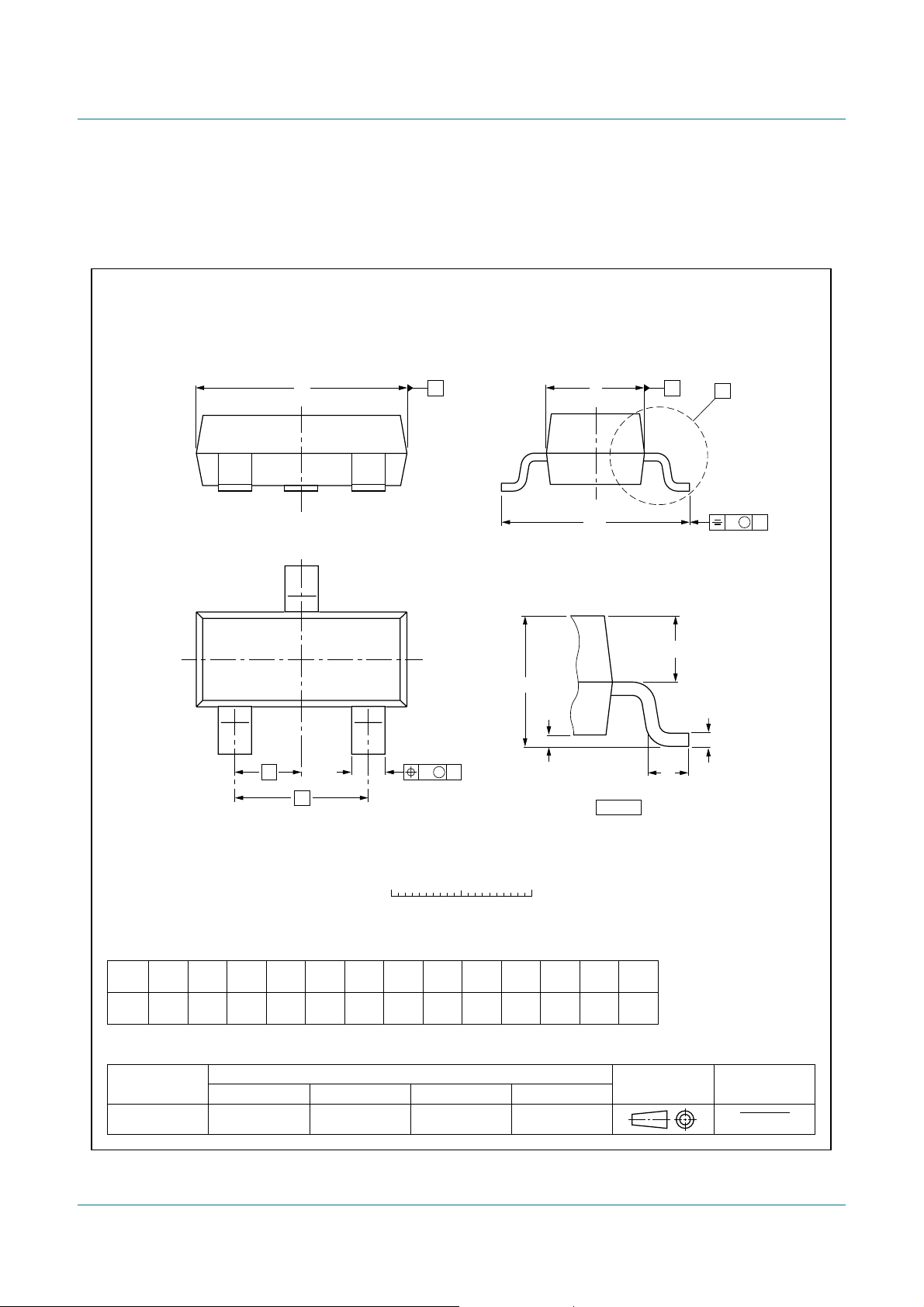
Plastic surface-mounted package; 3 leads SOT23
D
3
A
A
1
12
e
1
b
p
e
w M
B
E
H
E
detail X
AB
Q
L
p
X
v M
A
c
0 1 2 mm
scale
DIMENSIONS (mm are the original dimensions)
A
UNIT
1.1
mm
0.9
OUTLINE
VERSION
SOT23 TO-236AB
1
A
max.
0.1
cD
b
p
0.48
0.15
0.38
0.09
IEC JEDEC JEITA
3.0
2.8
E
1.4
1.2
REFERENCES
1.9
e
e
0.95
H
L
Qwv
1
2.5
2.1
p
E
0.55
0.45
0.15
0.45
0.2
0.1
EUROPEAN
PROJECTION
ISSUE DATE
04-11-04
06-03-16
Fig 11. Package outline SOT23 (TO-236AB)
PDTA144V_SER_4 © NXP B.V. 2009. All rights reserved.
Product data sheet Rev. 04 — 3 September 2009 13 of 18
Page 14
NXP Semiconductors
PDTA144V series
PNP resistor-equipped transistors; R1 = 47 kΩ, R2 = 10 kΩ
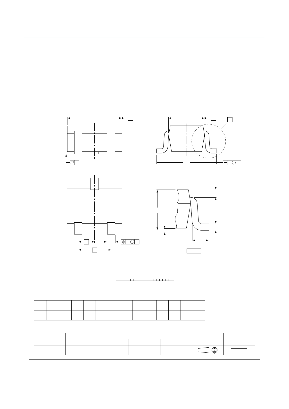
Plastic surface-mounted package; 3 leads SOT323
D
y
3
A
12
e
b
1
p
e
w M
B
E
H
E
A
1
detail X
AB
L
p
X
v M
A
Q
c
0 1 2 mm
scale
DIMENSIONS (mm are the original dimensions)
A
1
UNIT
A
1.1
mm
0.8
OUTLINE
VERSION
SOT323 SC-70
max
0.1
b
cD
p
0.4
0.25
2.2
0.3
0.10
IEC JEDEC JEITA
1.8
1.35
1.15
e
E
1.3
REFERENCES
e1H
0.65
2.2
2.0
L
Qwv
p
E
0.45
0.15
0.23
0.13
0.20.2
EUROPEAN
PROJECTION
ISSUE DATE
04-11-04
06-03-16
Fig 12. Package outline SOT323 (SC-70)
PDTA144V_SER_4 © NXP B.V. 2009. All rights reserved.
Product data sheet Rev. 04 — 3 September 2009 14 of 18
Page 15

NXP Semiconductors
9. Packing information
PDTA144V series
PNP resistor-equipped transistors; R1 = 47 kΩ, R2 = 10 kΩ
Table 9. Packing methods
The indicated -xxx are the last three digits of the 12NC ordering code.
Type number Package Description Packing quantity
PDTA144VE SOT416 4 mm pitch, 8 mm tape and reel -115 - -135
PDTA144VK SOT346 4 mm pitch, 8 mm tape and reel -115 - -135
PDTA144VM SOT883 2 mm pitch, 8 mm tape and reel - - -315
PDTA144VS SOT54 bulk, straight leads - -412 -
SOT54A tape and reel, wide pitch - - -116
tape ammopack, wide patch - - -126
SOT54 variant bulk, delta pinning - -112 PDTA144VT SOT23 4 mm pitch, 8 mm tape and reel -215 - -235
PDTA144VU SOT323 4 mm pitch, 8 mm tape and reel -115 - -135
[1] For further information and the availability of packing methods, seeSection 12.
[1]
3000 5000 10000
PDTA144V_SER_4 © NXP B.V. 2009. All rights reserved.
Product data sheet Rev. 04 — 3 September 2009 15 of 18
Page 16

NXP Semiconductors
PNP resistor-equipped transistors; R1 = 47 kΩ, R2 = 10 kΩ
PDTA144V series
10. Revision history
Table 10. Revision history
Document ID Release date Data sheet status Change notice Supersedes
PDTA144V_SER_4 20090903 Product data sheet - PDTA144V_SER_3
Modifications:
PDTA144V_SER_3 20050222 Product data sheet - PDTA144VT_2
PDTA144VT_2 20040514 Objective data sheet - PDTA144VT_1
PDTA144VT_1 20040305 Objective data sheet - -
• This data sheet was changed to reflect the new company name NXP Semiconductors,
including new legal definitions and disclaimers. No changes were made to the technical
content
• Figure 5 “Package outline SOT416 (SC-75)”:updated
• Figure 6 “Package outline SOT346 (SC-59A/TO-236)”: updated
• Figure 11 “Package outline SOT23 (TO-236AB)”: updated
• Figure 12 “Package outline SOT323 (SC-70)”: updated
PDTA144V_SER_4 © NXP B.V. 2009. All rights reserved.
Product data sheet Rev. 04 — 3 September 2009 16 of 18
Page 17

NXP Semiconductors
11. Legal information
11.1 Data sheet status
PDTA144V series
PNP resistor-equipped transistors; R1 = 47 kΩ, R2 = 10 kΩ
Document status
Objective [short] data sheet Development This document contains data from the objective specification for product development.
Preliminary [short] data sheet Qualification This document contains data from the preliminary specification.
Product [short] data sheet Production This document contains the product specification.
[1] Please consult the most recently issued document before initiating or completing a design.
[2] The term ‘short data sheet’ is explained in section “Definitions”.
[3] The product status of device(s) described in this document mayhave changed since this document was published and may differ in case of multiple devices. The latest product status
information is available on the Internet at URL
[1][2]
Product status
11.2 Definitions
Draft — The document is a draft version only. The content is still under
internal review and subject to formal approval, which may result in
modifications or additions. NXP Semiconductors does not give any
representations or warranties as to the accuracy or completeness of
information included herein and shall haveno liability for the consequences of
use of such information.
Short data sheet — A short data sheet is an extract from a full data sheet
with the same product type number(s) and title. Ashort data sheet is intended
for quick reference only and should not be relied upon tocontain detailedand
full information. For detailed and full information see the relevant full data
sheet, which is available on request via the local NXP Semiconductors sales
office. In case of any inconsistency or conflict with the short data sheet, the
full data sheet shall prevail.
11.3 Disclaimers
General — Information in this document is believed to be accurate and
reliable. However, NXP Semiconductors does not give any representations or
warranties, expressedor implied,as to theaccuracy or completenessof such
information and shall have no liability for the consequences of use of such
information.
Right to make changes — NXP Semiconductors reserves the right to make
changes to information published in this document, including without
limitation specifications and product descriptions, at any time and without
notice. This document supersedes and replaces allinformation suppliedprior
to the publication hereof.
Suitability for use — NXP Semiconductors products are not designed,
authorized or warranted to be suitable for use in medical, military, aircraft,
space or life support equipment, nor in applications where failure or
malfunction of an NXP Semiconductors product can reasonably be expected
to result in personal injury, death or severe property or environmental
[3]
http://www.nxp.com.
Definition
damage. NXP Semiconductors accepts no liability for inclusion and/or use of
NXP Semiconductors products in such equipment or applications and
therefore such inclusion and/or use is at the customer’s own risk.
Applications — Applications that are described herein for any of these
products are for illustrative purposes only. NXP Semiconductors makes no
representation or warranty that such applications will be suitable for the
specified use without further testing or modification.
Limiting values — Stress above one or more limiting values (as defined in
the Absolute Maximum Ratings System of IEC 60134)may cause permanent
damage to the device. Limiting values are stress ratings only and operation of
the device at these or any other conditions above those given in the
Characteristics sections of this document is not implied. Exposure to limiting
values for extended periods may affect device reliability.
Terms and conditions of sale — NXP Semiconductors products are sold
subject to the general terms and conditions of commercial sale, as published
at
http://www.nxp.com/profile/terms, including those pertaining to warranty,
intellectual property rights infringement and limitation of liability, unless
explicitly otherwise agreed to in writing by NXP Semiconductors. In case of
any inconsistency or conflict between information in this document and such
terms and conditions, the latter will prevail.
No offer to sell or license — Nothing in this document may be interpreted
or construed as an offer to sell products that is open for acceptance or the
grant, conveyanceor implication of any license under any copyrights, patents
or other industrial or intellectual property rights.
Export control — This document as well as the item(s) described herein
may be subject to export control regulations. Export might require a prior
authorization from national authorities.
Quick reference data — The Quick reference data is an extract of the
product data given in the Limiting values and Characteristics sections of this
document, and as such is not complete, exhaustive or legally binding.
11.4 Trademarks
Notice: All referencedbrands, product names, service names and trademarks
are the property of their respective owners.
12. Contact information
For more information, please visit: http://www.nxp.com
For sales office addresses, please send an email to: [email protected]
PDTA144V_SER_4 © NXP B.V. 2009. All rights reserved.
Product data sheet Rev. 04 — 3 September 2009 17 of 18
Page 18

NXP Semiconductors
PNP resistor-equipped transistors; R1 = 47 kΩ, R2 = 10 kΩ
13. Contents
1 Product profile . . . . . . . . . . . . . . . . . . . . . . . . . . 1
1.1 General description. . . . . . . . . . . . . . . . . . . . . . 1
1.2 Features . . . . . . . . . . . . . . . . . . . . . . . . . . . . . . 1
1.3 Applications . . . . . . . . . . . . . . . . . . . . . . . . . . . 1
1.4 Quick reference data. . . . . . . . . . . . . . . . . . . . . 1
2 Pinning information. . . . . . . . . . . . . . . . . . . . . . 2
3 Ordering information. . . . . . . . . . . . . . . . . . . . . 3
4 Marking. . . . . . . . . . . . . . . . . . . . . . . . . . . . . . . . 3
5 Limiting values. . . . . . . . . . . . . . . . . . . . . . . . . . 4
6 Thermal characteristics. . . . . . . . . . . . . . . . . . . 4
7 Characteristics. . . . . . . . . . . . . . . . . . . . . . . . . . 5
8 Package outline . . . . . . . . . . . . . . . . . . . . . . . . . 7
9 Packing information. . . . . . . . . . . . . . . . . . . . . 15
10 Revision history. . . . . . . . . . . . . . . . . . . . . . . . 16
11 Legal information. . . . . . . . . . . . . . . . . . . . . . . 17
11.1 Data sheet status . . . . . . . . . . . . . . . . . . . . . . 17
11.2 Definitions. . . . . . . . . . . . . . . . . . . . . . . . . . . . 17
11.3 Disclaimers. . . . . . . . . . . . . . . . . . . . . . . . . . . 17
11.4 Trademarks. . . . . . . . . . . . . . . . . . . . . . . . . . . 17
12 Contact information. . . . . . . . . . . . . . . . . . . . . 17
13 Contents . . . . . . . . . . . . . . . . . . . . . . . . . . . . . . 18
PDTA144V series
Please be aware that important notices concerning this document and the product(s)
described herein, have been included in section ‘Legal information’.
© NXP B.V. 2009. All rights reserved.
For more information, please visit: http://www.nxp.com
For sales office addresses, please send an email to: [email protected]
Date of release: 3 September 2009
Document identifier: PDTA144V_SER_4
 Loading...