

Philips PDIUSBP11AD, PDIUSBP11ADB Datasheet

INTEGRATED CIRCUITS
PDIUSBP11A
Universal Serial Bus Transceiver
Product specification
Supersedes data of 1997 Aug 01
1999 Jun 04
Philips Semiconductors Product specification
PDIUSBP1 1AUniversal Serial Bus transceiver
FEA TURES
•Complies with Universal Serial Bus specification 1.1
•Utilizes digital inputs and outputs to transmit and receive USB
cable data
•Supports 12Mbit/s “Full Speed” and 1.5Mbit/s “Low Speed” serial
data transmission
•Compatible with the VHDL “Serial Interface Engine” from USB
Implementers’ Forum
•Supports single-ended data interface
•Single 3.3V supply
DESCRIPTION
The PDIUSBP11A is a one chip generic USB transceiver. It is
designed to allow 5.0V or 3.3V programmable and standard logic to
interface with the physical layer of the Universal Serial Bus. It is
capable of transmitting and receiving serial data at both full speed
(12Mbit/s) and low speed (1.5Mbit/s) data rates.
The pinout conforms with the ”Serial Interface Engine”.
Implementation of the Serial Interface Engine along with the USB
transceiver allows the designer to make USB compatible devices
with off-the-shelf logic and easily modify and update the application.
The PDIUSBP11A is backward compatible to the PDIUSBP11 and
allows for single-ended data interfacing.
•Available in SO-14, SSOP-14 and TSSOP-14 packages
ORDERING INFORMATION
PACKAGES TEMPERATURE RANGE OUTSIDE NORTH AMERICA NORTH AMERICA PKG. DWG. #
14-pin plastic SO –40°C to +85°C PDIUSBP11A D PDIUSBP11A D SOT108-1
14-pin plastic SSOP –40°C to +85°C PDIUSBP11A DB PDIUSBP11A DB SOT337-1
14-pin plastic TSSOP –40°C to +85°C PDIUSBP11APW PDUSBP11APW DH SOT402-1
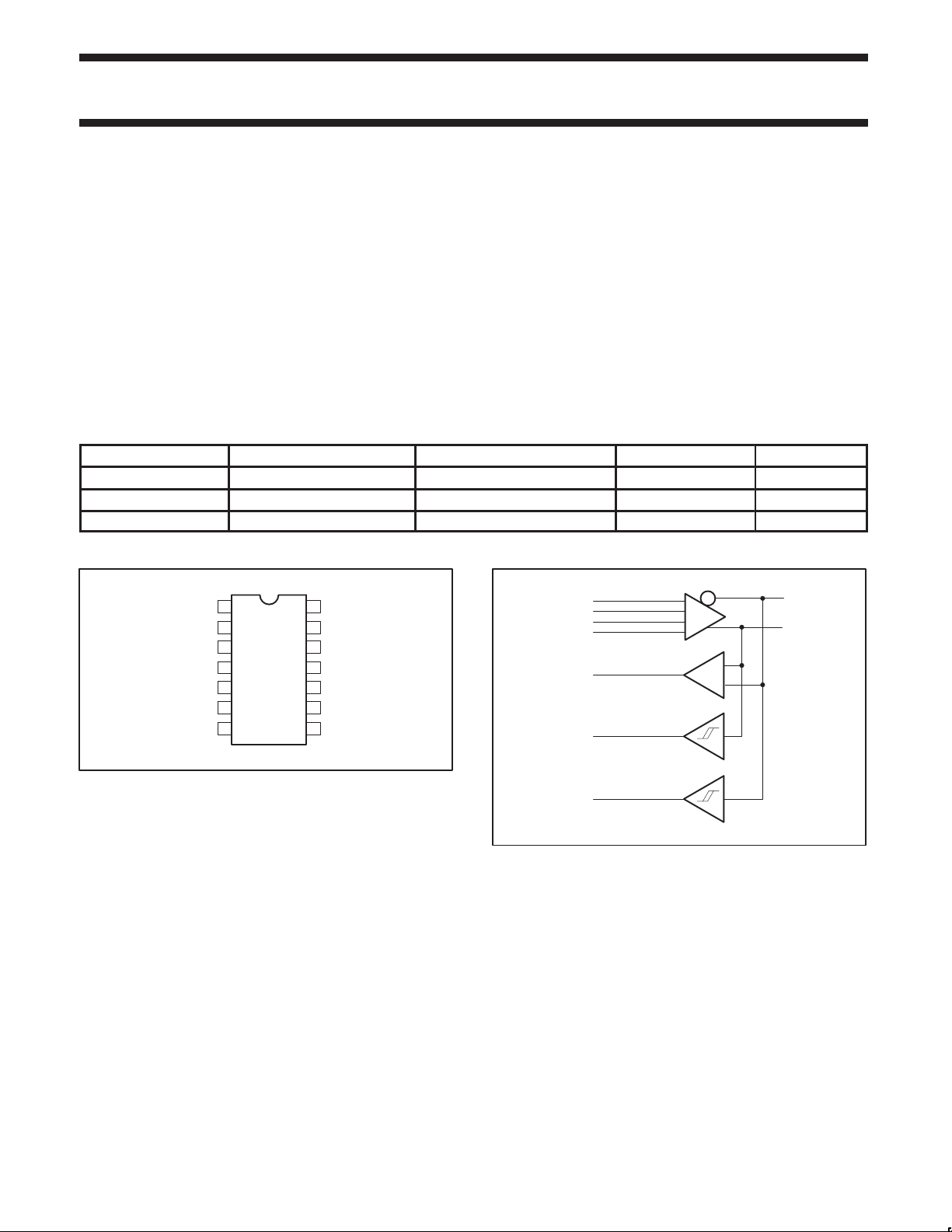
PIN CONFIGURATION
1
MODE
2
OE#
3
RCV
4
VP
5
VM
SUSPND
6
7
GND NC
14
13
12
11
10
9
8
V
CC
VMO/FSEO
VPO
D
D–
SPEED
FUNCTIONAL DIAGRAM
OE#
SPEED
VMO/FSEO
VPO
RCV
VP
D–
D+
+
–
SV00559
VM
SV00560
1999 Jun 04 853-2008 21712
2

Philips Semiconductors Product specification
12, 13
V
PO
VMO/F
SEO
I
PDIUSBP11AUniversal Serial Bus transceiver
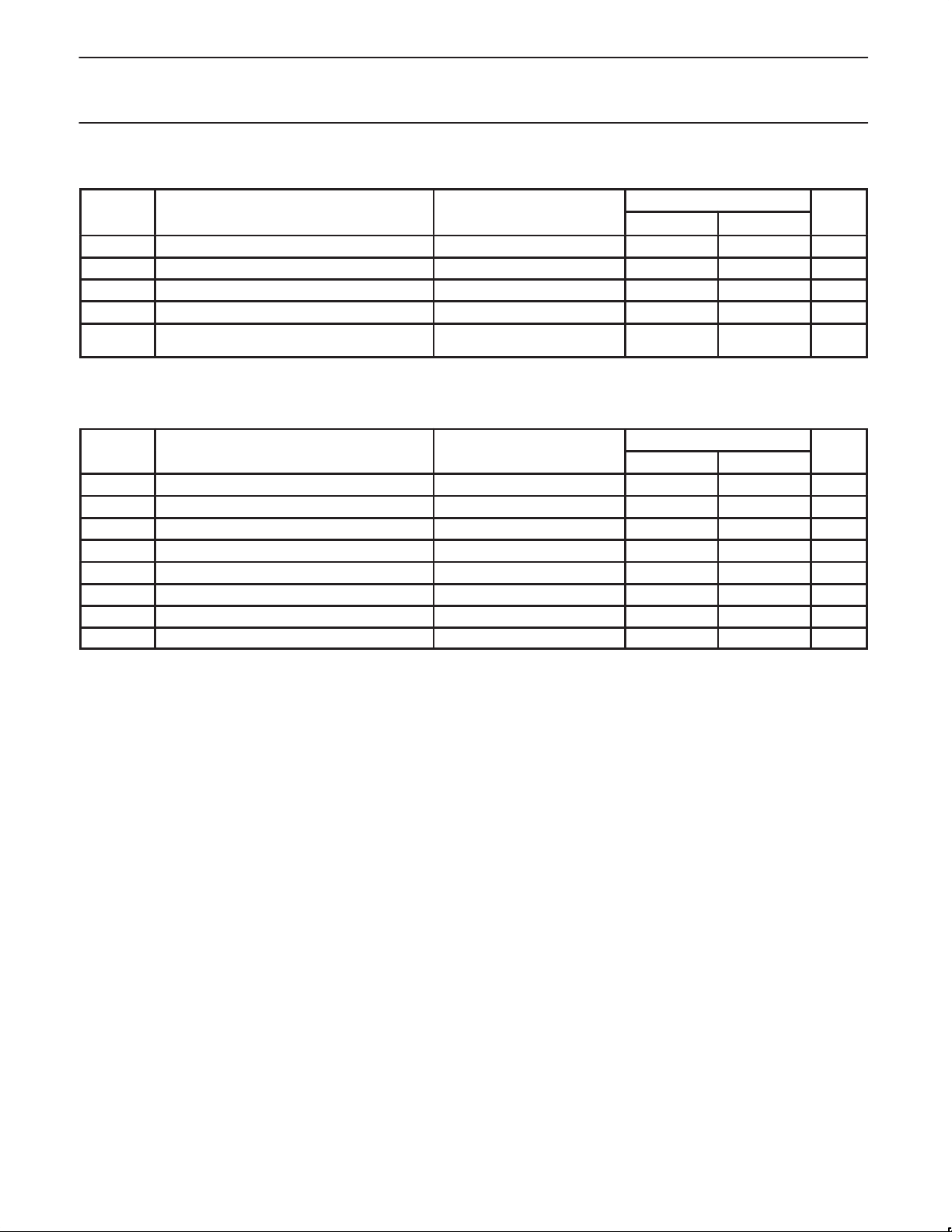
PIN DESCRIPTION
PIN
No.
3 RCV O Receive data. CMOS level output for USB differential input
2 OE# I
1 MODE I
4, 5 VP, V
11, 10 D+, D– AI/O Data+, Data–. Differential data bus conforming to the Universal Serial Bus standard.
6 SUSPND I
9 SPEED I
14 V
7 GND Ground reference
PIN
SYMBOL
,
M
CC
I/O NAME AND FUNCTION
Output Enable. Active LOW, enables the transceiver to transmit data on the bus.
When not active the transceiver is in receive mode
Mode. When left unconnected, a weak pull-up transistor pulls it to VCC and in this
mode, the PDIUSBP11A is backward compatible to PDIUSBP11. When connected to
GND, the VMO/FSEO pin takes the function of FSEO (Force SEO).
Inputs to differential driver. (Outputs from SIE).
MODE VPO VMO/FSEO RESULT
0 0 0 Logic “0”
0 1 SE0#
1 0 Logic “1”
1 1 SEO#
1 0 0 SE0#
0 1 Logic “0”
1 0 Logic “1”
1 1 Illegal code
Gated version of D– and D+. Outputs are logic “0” and logic “1”. Used to detect single
ended zero (SE0#), error conditions, and interconnect speed. (Inputs to SIE).
VP VM RESULT
O
0 0 SE0#
0 1 Low Speed
1 0 Full Speed
1 1 Error
Suspend. Enables a low power state while the USB bus is inactive. While the suspnd
pin is active it will drive the RCV pin to a logic “0” state. Both D+ and D– are tri-stated.
Edge rate control. Logic “1” operates at edge rates for “full speed”. Logic “0” operates
edge rates for “low speed”.
3.0V to 3.6V power supply
1999 Jun 04
3
Philips Semiconductors Product specification
SYMBOL
PARAMETER
CONDITIONS
UNIT
MIN.MAX
SYMBOL
PARAMETER
CONDITIONS
UNIT
PDIUSBP11AUniversal Serial Bus transceiver
RECOMMENDED OPERATING CONDITIONS
LIMITS
.
V
T
V
CC
V
AI/O
V
amb
DC supply voltage 3.0 3.6 V
DC Input voltage range 0 5.5 V
I
DC input range for AI/O’s 0 V
DC output voltage range 0 V
O
Operating ambient temperature range in free air
See DC and AC characteristics
per device
–40 +85 °C
CC
CC
V
V
ABSOLUTE MAXIMUM RATINGS
1
In accordance with the Absolute Maximum Rating System (IEC 134) Voltages are referenced to GND (ground = 0V)
LIMITS
MIN MAX
V
I
latchup
V
ICC, I
T
P
CC
V
I/O
V
STO
TOT
DC supply voltage –0.5 +6.5 V
Latchup current VI < 0 or VI > V
DC input voltage Note 2 –0.5 +5.5 V
I
CC
DC input voltage range for I/O’s –0.5 V
DC output voltage Note 2 –0.5 VCC +0.5 V
O
DC VCC or GND current – ±100 mA
GND
– 200 mA
CC
Storage temperature range –60 +150 °C
Power dissipation per package mW
+0.5 V
NOTES:
1. Stresses beyond those listed may cause permanent damage to the device. These are stress ratings only and functional operation of the
device at these or any other conditions beyond those indicated under “recommended operating conditions” is not implied. Exposure to
absolute-maximum-rated conditions for extended periods may affect device reliability .
2. The input and output voltage ratings may be exceeded if the input and output clamp current ratings are observed.
1999 Jun 04
4
 Loading...