

Philips PDIUSBP1 Service Manual
,
VMO
Philips Semiconductors Product specification
PDIUSBP1 1Universal Serial Bus transceiver
FEA TURES
•Utilizes digital inputs and outputs to transmit and receive USB
cable data
•Supports 12Mbit/s “Full Speed” and 1.5Mbit/s “Low Speed” serial
data transmission
•Compatible with the VHDL “Serial Interface Engine” from USB
developer’s conference
•Available in SO, 14 pin package
•Hysteresis on D+, D-, V
MO
inputs
DESCRIPTION
The PDIUSBP11 is a one chip generic USB transceiver. It is
designed to allow 5.0V or 3.3V programmable and standard logic to
interface with the physical layer of the Universal Serial Bus. It is
capable of transmitting and receiving serial data at both full speed
(12Mbit/s) and low speed (1.5Mbit/s) data rates. The outputs from
the serial interface engine (inputs VPO
PDIUSBP11) are driven by the host. The gated inputs (outputs VP
and VM on the PDIUSBP11) are to be decoded by the host.
Implementation of the Serial Interface Engine along with the USB
transceiver allow the designer to make flexible USB compatible
devices with widely available logic components.
and VMO on the
ORDERING INFORMATION
PACKAGES TEMPERATURE RANGE OUTSIDE NORTH AMERICA NORTH AMERICA PKG. DWG. #
14-pin plastic SO 0°C to +70°C PDIUSBP11 D PDIUSBP11 D SOT108-1
14-pin plastic SSOP 0°C to +70°C PDIUSBP11 DB PDIUSBP11 DB SOT337-1
14-pin plastic TSSOP 0°C to +70°C PDIUSBP11 PW PDUSBP11 PW DH SOT402-1
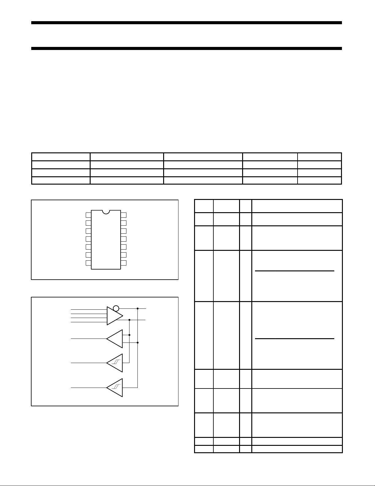
PIN CONFIGURA TION
1
NC
2
OE#
3
RCV
4
VP
5
VM
SUSPND
6
7
GND NC
FUNCTIONAL DIAGRAM
OE#
SPEED
VMO
VPO
RCV
VP
VM
14
V
CC
13
VMO
12
VPO
11
D
10
D–
9
SPEED
8
SV00142
D–
D+
+
–
SV00143
PIN DESCRIPTION
PIN
No.
3 RCV O
2 OE# I
12, 13
4, 5 VP, VM O
11, 10 D+, D– I/O
6 SUSPND I
9 SPEED I
14 V
7 GND Ground reference
PIN
SYMBOL
VPO,
CC
I/O NAME AND FUNCTION
Receive data. CMOS level output for
USB differential input
Output Enable. Active LOW, enables
the transceiver to transmit data on
the bus. When not active the
transceiver is in receive mode
Inputs to differential driver . (Outputs
from SIE).
VPO VMO RESULT
I
0 0 SE0#
0 1 Logic “0”
1 0 Logic “1”
1 1 Undefined
Gated version of D– and D+. Outputs
are logic “0” and logic “1”. Used to
detect single ended zero (SE0#),
error conditions, and interconnect
speed. (Inputs to SIE).
VP VM RESULT
0 0 SE0#
0 1 Full Speed
1 0 Low Speed
1 1 Error
Data+, Data–. Differential data bus
conforming to the Universal Serial
Bus standard.
Suspend. Enables a low power state
while the USB bus is inactive. While
the suspnd pin is active it will drive
the RCV pin to a logic “0” state.
Edge rate control. Logic “1” operates
at edge rates for “full speed”. Logic
“0” operates edge rates for “low
speed”.
3.0V to 3.6V power supply
1996 May 29 853-1836 16862
2

Philips Semiconductors Product specification
SYMBOL
PARAMETER
CONDITIONS
UNIT
MIN.MAX
SYMBOL
PARAMETER
CONDITIONS
UNIT
PDIUSBP11Universal Serial Bus transceiver
RECOMMENDED OPERATING CONDITIONS
LIMITS
.
T
V
V
CC
V
I/O
V
amb
DC supply voltage 3.0 3.6 V
DC Input voltage range 0 5.5 V
I
DC input range for I/O’s 0 V
DC output voltage range 0 V
O
Operating ambient temperature range in
free air
See DC and AC characteristics
for individual device
0 +70 °C
CC
CC
V
V
ABSOLUTE MAXIMUM RATINGS
1, 2
In accordance with the Absolute Maximum Rating System (IEC 134) Voltages are referenced to GND (ground = 0V)
LIMITS
MIN MAX
I
GND
V
I
V
I
V
T
P
DC supply voltage –0.5 +6.5 V
CC
DC input diode current VI < 0 – –50 mA
IK
V
DC input voltage Note 3 –0.5 +5.5 V
I
DC input voltage range for I/O’s –0.5 V
I/O
DC output diode current VO > VCC or VO < 0 – 50 mA
OK
DC output voltage Note 3 –0.5 VCC +0.5 V
O
DC output source or sink current for VP/VM,
I
O
RCV pins
DC output source or sink current for D+/D–
I
O
pins
VO = 0 to V
VO = 0 to V
CC
CC
– 15 mA
– 50 mA
+0.5 V
CC
, ICCDC VCC or GND current – 100 mA
Storage temperature range –60 +150 °C
stg
Power dissipation per package mW
tot
NOTES:
1. Stresses beyond those listed may cause permanent damage to the device. These are stress ratings only and functional operation of the
device at these or any other conditions beyond those indicated under “recommended operating conditions” is not implied. Exposure to
absolute-maximum-rated conditions for extended periods may affect device reliability .
2. The performance capability of a high-performance integrated circuit in conjunction with its thermal environment can create junction
temperatures which are detrimental to reliability. The maximum junction temperature of this integrated circuit should not exceed 150°C.
3. The input and output voltage ratings may be exceeded if the input and output clamp current ratings are observed.
1996 May 29
3
 Loading...