

Philips PDIUSBH12D, PDIUSBH12N Datasheet

INTEGRATED CIRCUITS
PDIUSBH12
USB 2-port hub
Product specification
Supersedes data of 1999 Feb 25
1999 Jul 22

Philips Semiconductors Product specification
PDIUSBH12USB 2-port hub
FEA TURES
•Complies with the Universal Serial Bus specification Rev. 1.0
•Complies with the ACPI, OnNOW, and USB power management
requirements
•Compliant with USB Human Interface Devices and Monitor
Control Class
•Compliant with System Management Bus Specification Rev. 1.0
•Two downstream ports with per packet connectivity and auto
speed detection
•Supports up to 3 embedded functions
•Integrated SIE (Serial Interface Engine), FIFO memory and
transceivers
•Automatic USB protocol handling
•High speed slave I
2
C Interface (up to 1 Mbit/s)
•Compatible with the PDIUSBH11 hardware and software
•Software controllable connection to USB bus (SoftConnect)
•Good USB downstream connection indicators that blink with traffic
(GoodLink)
•Low frequency 12 MHz crystal oscillator eases EMI design issues
•Programmable output clock frequency
•Bus powered capability with very low suspend current
•Controllable LazyClock output at 30 kHz (nominal) during suspend
•Single 3.3V supply with 5V tolerant I/O
•Available in 28-pin DIP and SO packages
•Full-scan design with high fault coverage (>99%) insures high
quality
•Higher than 8 KV in-circuit ESD protection lowers cost of extra
components
DESCRIPTION
The Universal Serial Bus Hub PDIUSBH12 is a cost and feature
optimized second generation USB Hub with 2 downstream ports and
3 embedded functions (compound hub). It is normally used in any
microcontroller-based system and communicates with the system
microcontroller over the high speed I
approach to implementing a hub and embedded functions allows the
designer to choose the optimum system microcontroller from the
available wide variety. This flexibility cuts down the development
time, risks and costs by allowing the use of the existing architecture
and the firmware investments. This results in the fastest way to
develop the most cost-effective USB peripheral solutions that need
hub functionality. The PDIUSBH12 is ideally suited for computer
monitors, docking stations, keyboards and many other applications
that use the I
The PDIUSBH12 conforms to the USB specification Rev 1.0, I2C
serial interface and the SMBus specifications. It is fully compliant
with the Human Interface Device Class and Monitor Control Class
specifications. Its low suspend power consumption along with the
programmable LazyClock output allows for easy implementation of
equipment that is compliant to the ACPI, OnNow and USB power
management requirements. The low operating power allows the
implementation of the bus powered or the compound powered hub
function.
The PDIUSBH12 is fully backward compatible to the first generation
PDIUSBH11 hardware and software. This allows an easy running
change in the manufacturing line to realize the cost savings. In
addition, it also incorporates the feature enhancements like
SoftConnect
lower frequency crystal oscillator, additional embedded functions
and integration of termination resistors. All of these feature
enhancements contribute to significant cost savings in the system
implementation and at the same time ease the implementation of
advanced USB functionality into the peripherals.
2
C or the SMBus based architecture.
, GoodLink, LazyClock, programmable clock output,
2
C serial bus. This modular
ORDERING INFORMATION
PACKAGES TEMPERATURE RANGE OUTSIDE NORTH AMERICA NORTH AMERICA PKG. DWG. #
28-pin plastic SO –40°C to +85°C PDIUSBH12 D PDIUSBH12 D SOT136-1
28-pin plastic DIP –40°C to +85°C PDIUSBH12 N PDIUSBH12 N SOT117-1
1999 Jul 22 853-2062 22025
2
Philips Semiconductors Product specification
PDIUSBH12USB 2-port hub
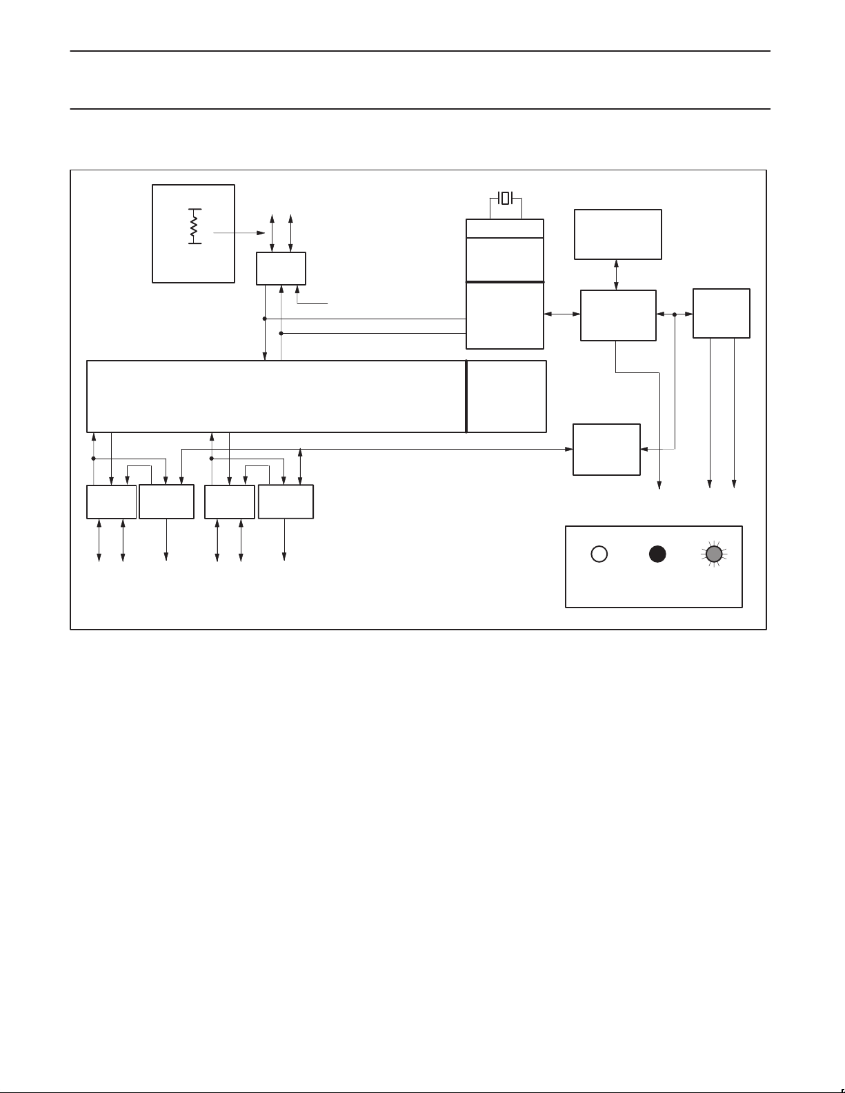
BLOCK DIAGRAM
UPSTREAM
3.3V
1.5kΩ
D+
SoftConnect
PORT
D+
ANALOG
TX/R
HUB
D–
X
FULL SPEED
REPEATER
ANALOG
T
X/RX
D–D+
DOWNSTREAM
PORT 2
GOODLINK
CONTROL
LED
ANALOG
T
X/RX
D–D+
DOWNSTREAM
PORT 3
GOODLINK
CONTROL
LED
NOTE:
1. This is a conceptual block diagram and does not include each individual signal.
12 MHz
PLL
BIT CLOCK
RECOVERY
PHILIPS
SIE
END OF
FRAME
TIMERS
INTEGRATED
RAM
MEMORY
MANAGEMENT
UNIT
GENERAL
PORT
CONTROLLER
INTERRUPT SDA SCL
NO LIGHT LIT BLINKING
NO
CONNECTION
CONNECTED
GOODLINK
I
SLAVE
INTERFACE
DATA
TRANSFER
SV00852
2
C
1999 Jul 22
3

Philips Semiconductors Product specification
PDIUSBH12USB 2-port hub
Analog Transceivers
These transceivers interface directly to the USB cables through
some termination resistors. They are capable of transmitting and
receiving serial data at both “full speed” (12 Mbit/s) and “low speed”
(1.5 Mbit/s) data rates.
Hub Repeater
The hub repeater is responsible for managing connectivity on a per
packet basis. It implements packet signaling connectivity and
resume connectivity.
Low speed devices can be connected to downstream ports since the
repeater will not propagate upstream packets to downstream ports,
to which low speed devices are connected, unless they are
preceded by a PREAMBLE PID.
End of Frame Timers
This block contains the specified EOF1 and EOF2 timers which are
used to detect loss-of-activity and babble error conditions in the hub
repeater. The timers also maintain the low-speed keep-alive strobe
which is sent at the beginning of a frame.
General and Individual Port Controller
The general and individual port controllers together provide status
and control of individual downstream ports. Via the I
microcontroller can access the downstream ports and request or
change the status of each individual port.
Any change in the status or settings of the individual port will result
in an interrupt request. Via an interrupt register, the servicing
microcontroller can look up the downstream port which generated
the interrupt and request its new status. Any port status change can
then be reported to the host via the hub status change (interrupt)
endpoint.
2
C-interface a
PLL
A 12 MHz to 48 MHz clock multiplier PLL (Phase-Locked Loop) is
integrated on-chip. This allows for the use of low-cost 12 MHz
crystal. EMI is also minimized due to lower frequency crystal. No
external components are needed for the operation of the PLL.
Bit Clock Recovery
The bit clock recovery circuit recovers the clock from the incoming
USB data stream using 4X over-sampling principle. It is able to track
jitter and frequency drift specified by the USB specification.
Philips Serial Interface Engine (PSIE)
The Philips SIE implements the full USB protocol layer. It is
completely hardwired for speed and needs no firmware intervention.
The functions of this block include: synchronization pattern
recognition, parallel/serial conversion, bit stuffing/de-stuffing, CRC
checking/generation, PID verification/generation, address
recognition, handshake evaluation/generation.
Memory Management Unit (MMU) and Integrated RAM
The MMU and the integrated RAM is used to handle the large
difference in data rate between USB, running in bursts of 12 Mbit/s
and the I
1 Mbit/s. This allows the microcontroller to read and write USB
packets at its own speed through I2C.
2
C interface to the microcontroller, running at up to
I2C Slave Interface
This block implements the necessary I2C interface protocol. A slave
2
I
C allows for simple micro-coding. An interrupt is used to alert the
microcontroller whenever the PDIUSBH12 needs attention. As a
2
slave I
C device, the PDIUSBH12 I2C clock: SCL is an input and is
controlled by the microcontroller. The I
Mbit/s.
2
C interface can run up to 1
SoftConnect
The connection to the USB is accomplished by bringing D+ (for
high-speed USB device) high through a 1.5 kΩ pull-up resistor. In
the PDIUSBH12, the 1.5 kΩ pull-up resistor is integrated on-chip
and is not connected to V
pull-down resistors are integrated on-chip and are not connected to
GND by default. The connection of the internal resistors to Vcc is
established through a command sent by the external/system
microcontroller. This allows the system microcontroller to complete
its initialization sequence before deciding to establish connection to
the USB. Re-initialization of the USB bus connection can also be
affected without requiring the pull out of the cable.
The PDIUSBH12 will check for USB VBUS availability before the
connection can be established. VBUS sensing is provided through
OCURRENT_N pin. See the pin description for details. Sharing of
VBUS sensing and overcurrent sensing can be easily accomplished
by using VBUS voltage as the pull-up voltage for the open drain
output of the overcurrent indication device.
It should be noted that the tolerance of the internal resistors is
higher (30%) than that specified by the USB specification (5%).
However, the overall V
can still be met with good margin. The decision to make use of this
feature lies with the users.
SoftConnect is a patent pending technology from Philips
Semiconductors.
by default. Similarly, the 15 kΩ
CC
voltage specification for the connection
SE
GoodLink
Good downstream USB connection indication is provided through
GoodLink
least one valid upstream traffic from the port, the LED indicator will
be ON. The LED indicator will blink on every valid upstream traffic. A
valid upstream traffic is defined as traffic with a good SOP and
terminated by a good EOP. During global suspend, all LEDs will be
OFF.
This feature provides a user-friendly indicator on the status of the
hub, the connected downstream devices and the USB traffic. It is a
useful field diagnostics tool to isolate the faulty equipment. This
feature helps lower the field support and the hotline costs.
technology . When the port is enabled and there is at
1999 Jul 22
4

Philips Semiconductors Product specification
01Control
2–3: Downstream
03Control
14Generic
1
27Generic
39Generic
01Control
2–3: Downstream
03Control
1
14Generic
011Control
6
17Generic
013Control
7
19Generic
PDIUSBH12USB 2-port hub
ENDPOINT DESCRIPTIONS
There are two endpoint configuration modes supported by the PDIUSBH12, the Single Embedded Function mode and the Multiple (3)
Embedded Function mode. The Single Embedded Function mode is the default at power up reset. The Multiple (3) Embedded Function mode
can be configured by writing a zero to bit 7 of the first byte of the Set Mode command. Either mode is backward compatible to the PDIUSBH11.
T able 1. SINGLE EMBEDDED FUNCTION MODE (DEFAULT AT POWER UP)
FUNCTION PORTS ENDPOINT #
Hub
Embedded
Function 1
NOTE:
1. Hub interrupt endpoint is not indexed.
2. Generic endpoint can be used for Interrupt or Bulk endpoint.
0: Upstream
ENDPOINT
INDEX
0
1
–
2
5
6
8
TRANSFER
TYPE
Interrupt
DIRECTION
OUT 8
IN 8
IN 1
OUT 8
IN 8
OUT 8
IN 8
OUT 8
IN 8
OUT 8
IN 8
MAX
PACKET SIZE
(BYTES)
T able 2. MULTIPLE (3) EMBEDDED FUNCTION MODE
FUNCTION PORTS ENDPOINT #
Hub
Embedded
Function 1
Embedded
Function 6
Embedded
Function 7
0: Upstream
1 – Interrupt IN 1
ENDPOINT
INDEX
0
2
5
10
6
12
8
TRANSFER
TYPE
DIRECTION
OUT 8
IN 8
OUT 8
IN 8
OUT 8
IN 8
OUT 8
IN 8
OUT 8
IN 8
OUT 8
IN 8
OUT 8
IN 8
MAX
PACKET SIZE
(BYTES)
1999 Jul 22
5

Philips Semiconductors Product specification
PDIUSBH12USB 2-port hub
PINNING
The PDIUSBH12 has two modes of operation. The first mode (Mode 0) configures the pins DNx_GL_N for GoodLink LED indication. The
second mode (Mode 1) configures the LED pins as per port overcurrent condition pins. An overcurrent condition on any port can be uniquely
identified in Mode 1. However, all downstream ports are disabled as a result of a single overcurrent condition. In addition to the two modes of
operation, the PDIUSBH12 can also be configured to take either a 48 MHz crystal oscillator (for backward compatibility to PDIUSBH11) or a 12
MHz crystal.
The internal 4X clock multiplier PLL will be activated when 12 MHz input XTAL mode is selected. Also, the output clock frequenc y is now
programmable rather than fixed to 12 MHz. The output clock frequency can be programmed through the Set Mode command. All these new
features are added while maintaining backward compatibility to the PDIUSBH11 through TEST2 and TEST1 pins.
TEST2 TEST1
00
01
10
11
MODE
MODE 0
(GoodLink)
MODE 0
(GoodLink)
MODE 1
(Individual Overcurrent)
MODE 1
(Individual Overcurrent)
NOTE:
1. Pin TEST3 should always be connected to Ground at all times.
Pin configuration
1
2
TEST2
3
TEST3
RESET_N
CLKOUT
OCURRENT_N /
OCURRENT2_N
SWITCH_N
DN3_GL_N /
OCURRENT3_N
4
5
GND
6
XTAL1
7
XTAL2
8
9
V
CC
10
11
12 17
13 16 RSVDDN2_GL_N
14 15 RSVD
NOTE:
Pin 10 and Pin 14 show alternative pin functions, depending on
mode of operation (Mode 0 or Mode 1) as described in
Pin Description
.
28TEST1
27
26
25
24
23
22
21
20
19
18
UP_DM
UP_DP
AV
CC
AGND
DN2_DM
DN2_DP
DN3_DM
DN3_DP
GND
SCL
SDA
INT_NSUSPEND
SV01751
INPUT XTAL FREQUENCY
(MHz)
48 12MHz
12 4 MHz
12 4 MHz
48 12 MHz
OUTPUT CLOCK FREQUENCY
(AT REST)
1999 Jul 22
6

Philips Semiconductors Product specification
PDIUSBH12USB 2-port hub
Pin description (MODE 0 – Good Link)
PIN NO. PIN SYMBOL TYPE DRIVE DESCRIPTION
1 TEST1 Input
2 TEST2 Input Connect to Ground
3 TEST3 Input Connect to Ground
4 RESET_N Input ST Power-on reset
5 GND Power Ground reference
6 XTAL1 Input Crystal connection 1 (48 or 12MHz depending on TEST1 pin)
7 XTAL2 Output Crystal connection 2 (48 or 12MHz depending on TEST1 pin)
8 CLKOUT Output 3mA Programmable output clock for external devices
9 V
10 OCURRENT_N Input ST
11 SWITCH_N Output OD6 Enables power to downstream ports
12 SUSPEND Output OD6 Device is in suspended state
13 DN2_GL_N Output OD6 Downstream port 2 GoodLink LED indicator
14 DN3_GL_N Output OD6 Downstream port 3 GoodLink LED indicator
15 RSVD Input Reserved. Connect to GND for normal operation.
16 RSVD Input Reserved. Connect to GND for normal operation.
17 INT_N Output OD6 Connect to microcontroller interrupt
18 SDA I/O OD6 I2C bi-directional data
19 SCL I/O OD6 I2C bit-clock
20 GND Power Ground reference
21 DN3_DP AI/O Downstream port 3 D+ connection
22 DN3_DM AI/O Downstream port 3 D– connection
23 DN2_DP AI/O Downstream port 2 D+ connection
24 DN2_DM AI/O Downstream port 2 D- connection
25 AGND Power Analog Ground reference
26 AV
27 UP_DP AI/O Upstream D+ connection
28 UP_DM AI/O Upstream D- connection
NOTE:
1. Signals ending in _N indicate active low signals.
ST: Schmitt Trigger
OD6: Open Drain with 6 mA drive
AI/O: Analog I/O
CC
CC
Power Voltage supply 3.3V ± 0.3V
Power Analog voltage supply 3.3V ± 0.3V
Connect to Ground for 48MHz crystal input.
Connect to VCC for 12MHz crystal input.
Over-current notice to the device. This pin is also used to sense the USB VBUS.
A LOW on this pin of less than 2 seconds is interpreted as an overcurrent notice;
longer than 2 seconds is interpreted as loss of VBUS.
1999 Jul 22
7

Philips Semiconductors Product specification
PDIUSBH12USB 2-port hub
Pin description (MODE 1 – Individual Overcurrent)
PIN NO PIN SYMBOL TYPE DRIVE DESCRIPTION
1 TEST1 Input
2 TEST2 Input Connect to V
3 TEST3 Input Connect to Ground
4 RESET_N Input ST Power-on reset
5 GND Power Ground reference
6 XTAL1 Input Crystal connection 1 (48 or 12MHz depending on TEST1 pin)
7 XTAL2 Output Crystal connection 2 (48 or 12MHz depending on TEST1 pin)
8 CLKOUT Output 3mA Programmable output clock for external devices
9 V
10 OCURRENT2_N Input ST
11 SWITCH_N Output OD6 Enables power to downstream ports
12 SUSPEND Output OD6 Device is in suspended state
13 DN2_GL_N Output OD6 Downstream port 2 GoodLink LED indicator
14 OCURRENT3_N Input ST Downstream port 3 over-current notice
15 RSVD Input Reserved. Connect to GND for normal operation.
16 RSVD Input Reserved. Connect to GND for normal operation.
17 INT_N Output OD6 Connect to microcontroller interrupt
18 SDA I/O OD6 I2C bi-directional data
19 SCL I/O OD6 I2C bit-clock
20 GND Power Ground reference
21 DN3_DP AI/O Downstream port 3 D+ connection
22 DN3_DM AI/O Downstream port 3 D– connection
23 DN2_DP AI/O Downstream port 2 D+ connection
24 DN2_DM AI/O Downstream port 2 D- connection
25 AGND Power Analog Ground reference
26 AV
27 UP_DP AI/O Upstream D+ connection
28 UP_DM AI/O Upstream D- connection
NOTE:
1. Signals ending in _N indicate active low signals.
ST: Schmitt Trigger
OD6: Open Drain with 6 mA drive
AI/O: Analog I/O
CC
CC
Power Voltage supply 3.3V ± 0.3V
Power Analog voltage supply 3.3V ± 0.3V
Connect to VCC for 48MHz crystal input.
Connect to Ground for 12MHz crystal input.
CC
Downstream port 2 over-current notice. This pin is also use to sense the USB
VBUS. A LOW on this pin of less than 2 seconds is interpreted as an overcurrent
notice; longer than 2 seconds is interpreted as loss of VBUS.
1999 Jul 22
8
Philips Semiconductors Product specification
PDIUSBH12USB 2-port hub
APPLICATION DIAGRAM
USB
3.3V
UPSTREAM
12MHz
CLKOUT
H12
USB
5V
POWER SWITCH
AND
OVERCURRENT CIRCUIT
DOWNSTREAM
SWITCHED
5V
I2C Interface
The I2C bus is used to interface to an external microcontroller
needed to control the operation of the hub. For cost consideration,
the target system microcontroller can be shared and utilized for this
purpose. The PDIUSBH12 implements a slave I
the PDIUSBH12 needs to communicate with the microcontroller it
asserts an interrupt signal. The microcontroller services this interrupt
by reading the appropriate status register on the PDIUSBH12
through the I
refer to the
2
C bus. (For more information about the I2C serial bus,
I2C Handbook
, Philips order number 9397 750 00013).
The I2C interface on the PDIUSBH12 defines two types of
transactions:
1. command transaction
A command transaction is used to define which data (e.g., status
byte, buffer data, ...) will be read from / written to the USB
interface in the next data transaction. A data transaction usually
follows a command transaction.
2. data transaction
A data transaction reads data from / writes data to the USB
interface. The meaning of the data is dependent on the
command transaction which was sent before the data
transaction.
Two addresses are used to differentiate between command and
data transactions. Writing to the command address is interpreted as
a command, while reading from / writing to the data address is used
to transfer data between the PDIUSBH12 and the controller.
2
C interface. When
I2C
GOODLINK LED
µC
SV00853
ADDRESS TABLE
TYPE OF ADDRESS
Command 0011 011 (binary)
Data 0011 010 (binary)
PHYSICAL ADDRESS
(MSB to LSB)
Protocol
An I2C transaction starts with a ‘Start Condition’, followed by an
address. When the address matches either the command or data
address the transaction starts and runs until a ‘Stop Condition’ or
another ‘Start Condition’ (repeated start) occurs.
The command address is write-only and is unable to do a read. The
next bytes in the message are interpreted as commands. Several
command bytes can be sent after one command address. Each of
the command bytes is acknowledged and passed on to the Memory
Management Unit inside the PDIUSBH12.
When the start condition address matches the data address, the
next bytes are interpreted as data. When the RW bit in the address
indicates a ‘master writes data to slave’ (=‘0’) the bytes are received,
acknowledged and passed on to the Memory Management Unit. If
the RW bit in the address indicates a ‘master reads data from slave’
(=‘1’) the PDIUSBH12 will send data to the master. The I
must acknowledge all data bytes except the last one. In this way the
2
I
C interface knows when the last byte has been transmitted and it
then releases the SDA line so that the master controller can
generate the STOP condition.
Repeated start support allows another packet to be sent without
generating a Stop Condition.
Timing
2
The I
C interface in the PDIUSBH12 can support clock speeds up to
1MHz.
2
C-master
1999 Jul 22
9
 Loading...