

Philips PDIUSBD12D, PDIUSBD12PW Datasheet

1. Description
PDIUSBD12
USB interface device with parallel bus
Rev. 07 — 27 November 2001 Product data
The PDIUSBD12 is a cost and feature optimized USB device. It is normally used in
microcontroller based systems and communicates with the system microcontroller
over the high-speed general purpose parallel interface. It also supports local DMA
transfer.
This modular approach to implementing a USB interface allows the designer to
choose the optimum system microcontroller from the available wide variety. This
flexibility cuts down the development time, risks, and costs by allowing the use of the
existing architecture and minimize firmware investments. This results in the fastest
way to develop the most cost effective USB peripheral solution.
2. Features
The PDIUSBD12 fully conforms to the
to be compliant with most device class specifications: Imaging Class, Mass Storage
Devices, Communication Devices, Printing Devices, and Human Interface Devices.
As such, the PDIUSBD12 is ideally suited for many peripherals like Printer, Scanner,
External Mass Storage (Zip Drive), Digital Still Camera, etc. It offers an immediate
cost reduction for applications that currently use SCSI implementations.
The PDIUSBD12 low suspend power consumption along with the LazyClock output
allows for easy implementation of equipment that is compliant to the ACPI™,
OnNOW™, and USB power management requirements. The low operating power
allows the implementation of bus powered peripherals.
In addition, it also incorporates features like SoftConnect™, GoodLink™,
programmable clock output, low frequency crystal oscillator, and integration of
termination resistors. All of these features contribute to significant cost savings in the
system implementation and at the same time ease the implementation of advanced
USB functionality into the peripherals.
■ Complies with the
■ High performance USB interface device with integrated SIE, FIFO memory,
transceiver and voltage regulator
■ Compliant with most Device Class specifications
■ High-speed (2 Mbytes/s) parallel interface to any external microcontroller or
microprocessor
■ Fully autonomous DMA operation
■ Integrated 320 bytes of multi-configuration FIFO memory
■ Double buffering scheme for main endpoint increases throughput and eases
real-time data transfer
Universal Serial Bus specification Rev. 1.1
USB specification Rev. 1.1
. It is also designed
Philips Semiconductors
■ Data transfer rates: 1 Mbytes/s achievable in Bulk mode, 1 Mbits/s achievable in
■ Bus-powered capability with very good EMI performance
■ Controllable LazyClock output during suspend
■ Software controllable connection to the USB bus (SoftConnect™)
■ Good USB connection indicator that blinks with traffic (GoodLink™)
■ Programmable clock frequency output
■ Complies with the ACPI, OnNOW and USB power management requirements
■ Internal Power-on reset and low-voltage reset circuit
■ Available in SO28 and TSSOP28 pin packages
■ Full industrial grade operation from −40 to +85 °C
■ Higher than 8 kV in-circuit ESD protection lowers cost of extra components
■ Full-scan design with high fault coverage (>99%) ensures high quality
■ Operation with dual voltages:
■ Multiple interrupt modes to facilitate both bulk and isochronous transfers.
PDIUSBD12
USB interface device with parallel bus
Isochronous mode
3.3 ±0.3 V or extended 5 V supply range of 4.0 to 5.5 V
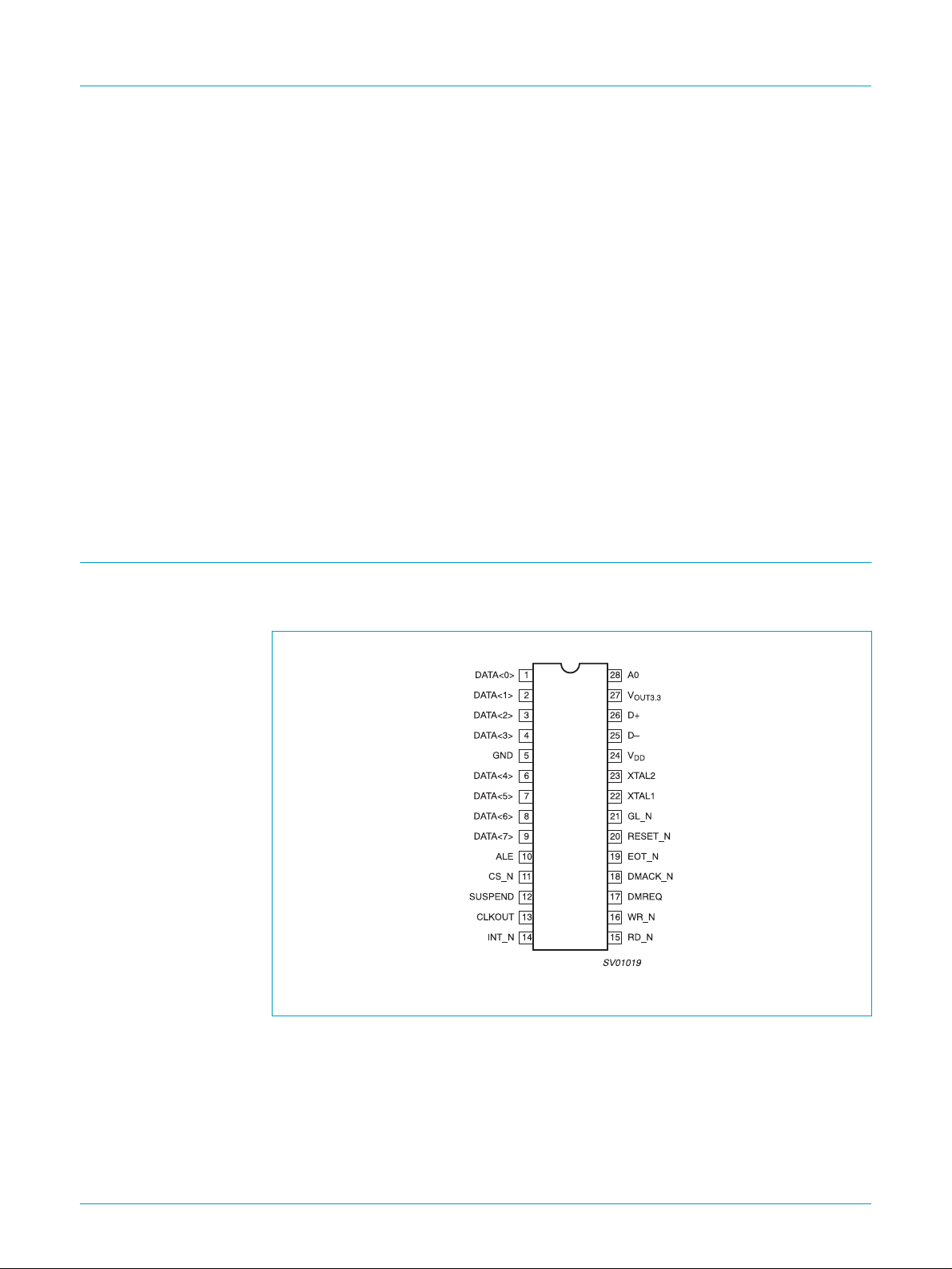
3. Pinning information
3.1 Pinning
Fig 1. Pin configuration.
9397 750 08969
Product data Rev. 07 — 27 November 2001 2 of 36
© Koninklijke Philips Electronics N.V. 2001. All rights reserved.

Philips Semiconductors
3.2 Pin description
Table 1: Pin description
Symbol Pin Type
DATA <0> 1 IO2 Bit 0 of bidirectional data. Slew-rate controlled.
DATA <1> 2 IO2 Bit 1 of bidirectional data. Slew-rate controlled.
DATA <2> 3 IO2 Bit 2 of bidirectional data. Slew-rate controlled.
DATA <3> 4 IO2 Bit 3 of bidirectional data. Slew-rate controlled.
GND 5 P Ground.
DATA <4> 6 IO2 Bit 4 of bidirectional data. Slew-rate controlled.
DATA <5> 7 IO2 Bit 5 of bidirectional data. Slew-rate controlled.
DATA <6> 8 IO2 Bit 6 of bidirectional data. Slew-rate controlled.
DATA <7> 9 IO2 Bit 7 of bidirectional data. Slew-rate controlled.
ALE 10 I Address Latch Enable. The falling edge is used to close the
CS_N 11 I Chip Select (Active LOW).
SUSPEND 12 I,OD4 Device is in Suspend state.
CLKOUT 13 O2 Programmable Output Clock (slew-rate controlled).
INT_N 14 OD4 Interrupt (Active LOW).
RD_N 15 I Read Strobe (Active LOW).
WR_N 16 I Write Strobe (Active LOW).
DMREQ 17 O4 DMA Request.
DMACK_N 18 I DMA Acknowledge (Active LOW).
EOT_N 19 I End ofDMA Transfer(Active LOW). Double up as V
RESET_N 20 I Reset (Active LOW and asynchronous). Built-in Power-onreset
GL_N 21 OD8 GoodLink LED indicator (Active LOW)
XTAL1 22 I Crystal Connection 1 (6 MHz).
XTAL2 23 O Crystal Connection 2 (6 MHz). If external clock signal, instead
V
CC
D− 25 A USB D− data line.
D+ 26 A USB D+ data line.
USB interface device with parallel bus
[1]
Description
latch of the address information in a multiplexed address/ data
bus. Permanently tied LOW for separate address/ data bus
configuration.
EOT_N is only valid when asserted together with DMACK_N
and either RD_N or WR_N.
circuit present on chip, so pin can be tied HIGH to V
of crystal, is connected to XTAL1, then XTAL2 should be
floated.
24 P Voltage supply (4.0 − 5.5 V).
To operate the IC at 3.3 V, supply 3.3 V to both V
pins.
PDIUSBD12
sensing.
BUS
.
CC
and V
CC
OUT3.3
9397 750 08969
Product data Rev. 07 — 27 November 2001 3 of 36
© Koninklijke Philips Electronics N.V. 2001. All rights reserved.
Philips Semiconductors
PDIUSBD12
USB interface device with parallel bus
Table 1: Pin description
Symbol Pin Type
V
OUT3.3
A0 28 I Address bit. A0 = 1 selects command instruction; A0 = 0 selects
[1] O2 : Output with 2 mA drive
OD4: Output Open Drain with 4 mA drive
OD8: Output Open Drain with 8 mA drive
IO2: Input and Output with 2 mA drive
O4: Output with 4 mA drive.
27 P 3.3 V regulated output. To operate the IC at 3.3 V, supply a
…continued
[1]
Description
3.3 V to both V
the data phase. This bit is a don’t care in a multiplexedaddress
and data bus configuration and should be tied HIGH.
CC
and V
OUT3.3
pins.
4. Ordering information
Table 2: Ordering information
Packages Temperature range Outside North America North America Pkg. Dwg. #
28-pin plastic SO −40 °C to +85 °C PDIUSBD12 D PDIUSBD12 D SOT136-1
28-pin plastic TSSOP −40 °C to +85 °C PDIUSBD12 PW PDIUSBD12PW DH SOT361-1
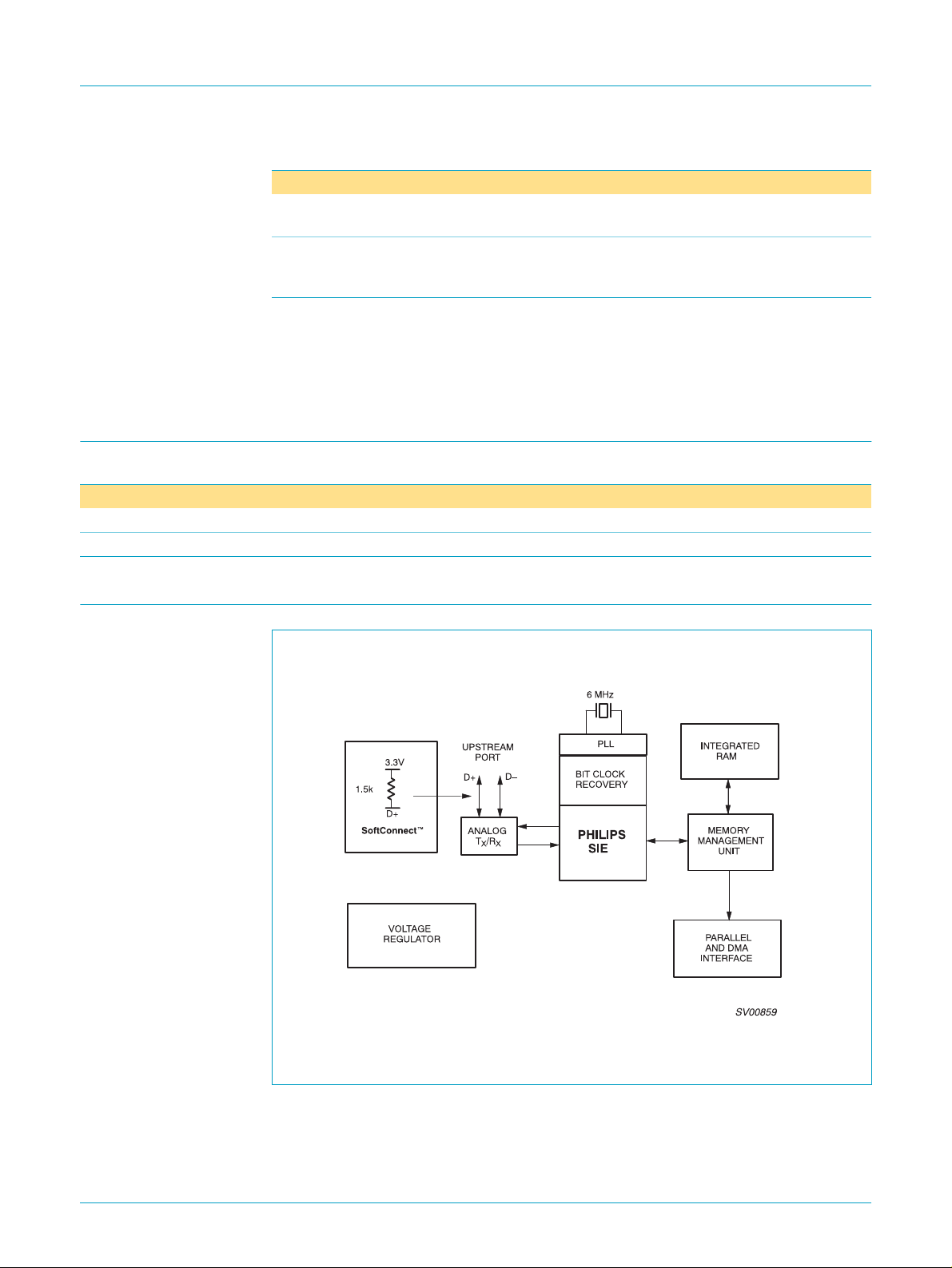
5. Block diagram
This is a conceptual block diagram and does not include each individual signal.
Fig 2. Block diagram.
9397 750 08969
Product data Rev. 07 — 27 November 2001 4 of 36
© Koninklijke Philips Electronics N.V. 2001. All rights reserved.

Philips Semiconductors
6. Functional description
6.1 Analog transceiver
The integrated transceiver interfaces directly to the USB cables through termination
resistors.
6.2 Voltage regulator
A 3.3 V regulator is integrated on-chip to supply the analog transceiver. This voltage
is also provided as an output to connect to the external 1.5 kΩ pull-up resistor.
Alternatively, the PDIUSBD12 provides SoftConnect technology with an integrated
1.5 kΩ pull-up resistor.
6.3 PLL
A 6 MHz to 48 MHz clock multiplier PLL (Phase-Locked Loop) is integrated on-chip.
This allows for the use of a low-cost 6 MHz crystal. EMI is also minimized due to the
lower frequency crystal. No external components are needed for the operation of the
PLL.
PDIUSBD12
USB interface device with parallel bus
6.4 Bit clock recovery
The bit clock recovery circuit recovers the clock from the incoming USB data stream
using 4× oversampling principle. It is able to track jitter and frequency drift specified
by the USB specification.
6.5 Philips Serial Interface Engine (PSIE)
The Philips SIE implements the full USB protocol layer. It is completely hardwired for
speed and needs no firmware intervention. The functions of this block include:
synchronization pattern recognition, parallel/serial conversion, bit stuffing/de-stuffing,
CRC checking/generation, PID verification/generation, address recognition, and
handshake evaluation/generation.
6.6 SoftConnect
The connection to the USB is accomplished by bringing D+ (for high-speed USB
device)HIGH through a 1.5 kΩ pull-up resistor. In the PDIUSBD12, the 1.5 kΩ pull-up
resistor is integrated on-chip and is not connected to VCC by default. The connection
is established through a command sent by the external/system microcontroller. This
allows the system microcontroller to complete its initialization sequence before
deciding to establish connection to the USB. Re-initialization of the USB bus
connection can also be performed without requiring to pull out the cable.
The PDIUSBD12 will check for USB V
established. V
description” for details. Sharing of V
accomplished by using V
open-drain output of the DMA controller pin.
sensing is provided through pin EOT_N. See Section 3.2 “Pin
BUS
voltage as the pull-up voltage for the normally
BUS
availability before the connection can be
BUS
sensing and EOT_N can be easily
BUS
9397 750 08969
Product data Rev. 07 — 27 November 2001 5 of 36
© Koninklijke Philips Electronics N.V. 2001. All rights reserved.

Philips Semiconductors
It should be noted that the tolerance of the internal resistors is higher (25%) than that
specified by the USB specification (5%). However, the overall VSE voltage
specification for the connection can still be met with good margin. The decision to
make sure of this feature lies with the users.
6.7 GoodLink
Good USB connection indication is provided through GoodLink technology. During
enumeration, the LED indicator will blink ON momentarily corresponding to the
enumeration traffic. When the PDIUSBD12 is successfully enumerated and
configured, the LED indicator will be permanently ON. Subsequent successful (with
acknowledgement) transfer to and from the PDIUSBD12 will blink OFF the LED.
During suspend, the LED will be OFF.
This feature provides a user-friendly indicator on the status of the USB device, the
connected hub and the USB traffic. It is a useful field diagnostics tool to isolate faulty
equipment. This feature helps lower field support and hotline costs.
6.8 Memory Management Unit (MMU) and Integrated RAM
PDIUSBD12
USB interface device with parallel bus
The MMU and the integrated RAM buffer the difference in speed between USB,
running in bursts of 12 Mbits/s and the parallel interface to the microcontroller. This
allows the microcontroller to read and write USB packets at its own speed.
6.9 Parallel and DMA Interface
A generic parallel interface is defined for ease-of-use, speed, and allows direct
interfacing to major microcontrollers. To a microcontroller, the PDIUSBD12 appears
as a memory device with 8-bit data bus and 1 address bit (occupying 2 locations).
The PDIUSBD12 supports both multiplexed and non-multiplexed address and data
bus. The PDIUSBD12 also supports DMA (Direct Memory Access) transfer which
allows the main endpoint (endpoint 2) to directly transfer to and from the local shared
memory. Both single-cycle and burst mode DMA transfers are supported.
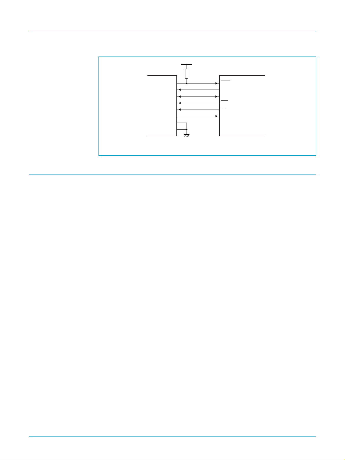
6.10 Example of parallel interface to an 80C51 microcontroller
In the example shown in Figure 3, the ALE pin is permanently tied LOW to signify a
separate address and data bus configuration. The A0 pin of the PDIUSBD12
connects to any of the 80C51 I/O ports. This port controls the command or data
phase to the PDIUSBD12. The multiplexed address and data bus of the 80C51 can
now be connected directly to the data bus of the PDIUSBD12. The address phase will
be ignored by the PDIUSBD12. The clock input signal of the 80C51 (pin XTAL1) can
be provided by output CLKOUT of the PDIUSBD12.
9397 750 08969
Product data Rev. 07 — 27 November 2001 6 of 36
© Koninklijke Philips Electronics N.V. 2001. All rights reserved.
Philips Semiconductors
PDIUSBD12
USB interface device with parallel bus
7. DMA transfer
PDIUSBD12
INT_N
A0
DATA [7:0
Fig 3. Example of a parallel interface to an 80C51 microcontroller.
]
WR_N
RD_N
CLKOUT
CS_N
ALE
INTO/P3.2
ANY I/O PORT (e.g. P3.3)
P [0.7:0.0]/AD [7:0
WR/P3.6
RD/P3.7
XTAL1
80C51
]
SV00870
Direct Memory Address (DMA) allows an efficient transfer of a block of data between
the host and local shared memory.Using a DMA controller, data transfer between the
PDIUSBD12’s main endpoint (endpoint 2) and local shared memory can happen
autonomously without local CPU intervention.
Preceding any DMA transfer, the local CPU receives from the host the necessary
setup information and programs the DMA controller accordingly. Typically, the DMA
controller is set up for demand transfer mode and the byte count register and the
address counter are programmed with the right values. In this mode, transfers occur
only when the PDIUSBD12 requests them and are terminated when the byte count
register reaches zero. After the DMA controller has been programmed, the DMA
enable bit of the PDIUSBD12 is set by the local CPU to initiate the transfer.
The PDIUSBD12 can be programmed for single-cycle DMA or burst mode DMA. In
single-cycle DMA, the DMREQ pin is deactivated for every single acknowledgement
by the DMACK_N before being re-asserted. In burst mode DMA, the DMREQ pin is
kept active for the number of bursts programmed in the device before going inactive.
This process continues until the PDIUSBD12 receives a DMA termination notice
through pin EOT_N. This will generate an interrupt to notify the local CPU that DMA
operation is completed.
For DMA read operation, the DMREQ pin will only be activated whenever the buffer is
full, signalling that the host has successfully transferred a packet to the PDIUSBD12.
With the double buffering scheme, the host can start filling up the second buffer while
the first buffer is being read out. This parallel processing increases the effective
throughput. When the host does not fill up the buffer completely (less than 64 bytes or
128 bytes for single direction ISO configuration), the DMREQ pin will be deactivated
at the last byte of the buffer regardless of the current DMA burst count. It will be
re-asserted on the next packet with a refreshed DMA burst count.
Similarly, for DMA write operations, the DMREQ pin remains active whenever the
buffer is not full. When the buffer is filled up, the packet is sent over to the host on the
next IN token and DMREQ will be reactivated if the transfer was successful. Also, the
double buffering scheme here will improve throughput. For non-isochronous transfer
(bulk and interrupt), the buffer needs to be completely filled up by the DMA write
9397 750 08969
Product data Rev. 07 — 27 November 2001 7 of 36
© Koninklijke Philips Electronics N.V. 2001. All rights reserved.

Philips Semiconductors
operation before the data is sent to the host. The only exception is at the end of DMA
transfer, when the reception of pin EOT_N will stop DMA write operation and the
buffer content will be sent to the host on the next IN token.
For isochronous transfers, the local CPU and DMA controller have to guarantee that
they are able to sink or source the maximum packet size in one USB frame (1 ms).
The assertion of pin DMACK_N automatically selects the main endpoint (endpoint 2),
regardless of the current selected endpoint. The DMA operation of the PDIUSBD12
can be interleaved with normal I/O access to other endpoints.
DMA operation can be terminated by resetting the DMA enable register bit or the
assertion of EOT_N together with DMACK_N and either RD_N or WR_N.
The PDIUSBD12 supports DMA transfer in single address mode and it can also work
in dual address mode of the DMA controller. In the single address mode, DMA
transfer is done via the DREQ, DMACK_N, EOT_N, WR_N and RD_N control lines.
In the dual address mode, pins DMREQ, DMACK_N and EOT_N are not used;
instead CS_N, WR_N and RD_N control signals are used. The I/O mode Transfer
Protocol of PDIUSBD12 needs to be followed. The source of the DMAC is accessed
during the read cycle and the destination during the write cycle. Transfer needs to be
done in two separate bus cycles, storing the data temporarily in the DMAC.
PDIUSBD12
USB interface device with parallel bus
8. Endpoint description
The PDIUSBD12 endpoints are sufficiently generic to be used by various device
classes ranging from Imaging, Printer, Mass Storage and Communication device
classes. The PDIUSBD12 endpoints can be configured for 4 operating modes
depending on the Set mode command. The 4 modes are:
Mode 0 Non-isochronous transfer (Non-ISO mode)
Mode 1 Isochronous output only transfer (ISO-OUT mode)
Mode 2 Isochronous input only transfer (ISO-IN mode)
Mode 3 Isochronous input and output transfer (ISO-I/O mode).
9397 750 08969
Product data Rev. 07 — 27 November 2001 8 of 36
© Koninklijke Philips Electronics N.V. 2001. All rights reserved.

Philips Semiconductors
Table 3: Endpoint Configuration
Endpoint
number
Mode 0 (Non-ISO mode)
0 0 Control OUT 16
1 2 Generic
2 4 Generic
Mode 1 (ISO-OUT mode)
0 0 Control OUT 16
1 2 Generic
2 4 Isochronous
Mode 2 (ISO-IN mode)
0 0 Control OUT 16
1 2 Generic
2 5 Isochronous
Mode 3 (ISO-I/O mode)
0 0 Control OUT 16
1 2 Generic
2 4 Isochronous
PDIUSBD12
USB interface device with parallel bus
Endpoint
Transfer type Direction
index
1IN16
[2]
OUT 16
3IN16
[2][3]
OUT 64
5IN64
1IN16
[2]
OUT 16
3IN16
[3]
OUT 128
1IN16
[2]
OUT 16
3IN16
[3]
IN 128
1IN16
[2]
OUT 16
3IN16
[3]
OUT 64
5IN64
[1]
Max. Packet
size (bytes)
[4]
[4]
[4]
[4]
[4]
[4]
[1] IN: input for the USB host; OUT: output from the USB host.
[2] Generic endpoints can be used either as Bulk or Interrupt endpoint.
[3] The main endpoint (endpoint number 2) is double-bufferedto ease synchronization with the real-time
applications and to increase throughput. This endpoint supports DMA access.
[4] Denotes double buffering. The size shown is for a single buffer.
9397 750 08969
Product data Rev. 07 — 27 November 2001 9 of 36
© Koninklijke Philips Electronics N.V. 2001. All rights reserved.

Philips Semiconductors
9. Main endpoint
The main endpoint (endpoint number 2) is the primary endpoint for sinking or
sourcing relatively large amounts of data. It implements the following features to ease
this task:
• Double buffering. This allows parallel operation between USB access and local
CPU access thus increasing throughput. Buffer switching is handled automatically.
This results in transparent buffer operation.
• DMA (Direct Memory Access) operation. This can be interleaved with normal I/O
operation to other endpoints.
• Automatic pointer handling during DMA operation. No local CPU intervention is
necessary when ‘crossing’ the buffer boundary.
• Configurableendpoint for either isochronous transfer or non-isochronous (bulk and
interrupt) transfer.
10. Command summary
PDIUSBD12
USB interface device with parallel bus
Table 4: Command summary
Name Destination Code (Hex) Transaction
Initialization commands
Set Address/Enable Device D0 Write 1 byte
Set Endpoint Enable Device D8 Write 1 byte
Set mode Device F3 Write 2 bytes
Set DMA Device FB Write/Read 1 byte
Data flow commands
Read Interrupt Register Device F4 Read 2bytes
Select Endpoint Control OUT 00 Read 1 byte (optional)
Control IN 01 Read 1 byte (optional)
Endpoint 1 OUT 02 Read 1 byte (optional)
Endpoint 1 IN 03 Read 1 byte (optional)
Endpoint 2 OUT 04 Read 1 byte (optional)
Endpoint 2 IN 05 Read 1 byte (optional)
Read Last Transaction Status Control OUT 40 Read 1 byte
Control IN 41 Read 1 byte
Endpoint 1 OUT 42 Read 1 byte
Endpoint 1 IN 43 Read 1 byte
Endpoint 2 OUT 44 Read 1 byte
Endpoint 2 IN 45 Read 1 byte
Read Buffer Selected Endpoint F0 Read nbytes
Write Buffer Selected Endpoint F0 Write n bytes
9397 750 08969
Product data Rev. 07 — 27 November 2001 10 of 36
© Koninklijke Philips Electronics N.V. 2001. All rights reserved.

Philips Semiconductors
PDIUSBD12
USB interface device with parallel bus
Table 4: Command summary
Name Destination Code (Hex) Transaction
Set Endpoint Status Control OUT 40 Write 1 byte
Acknowledge Setup Selected Endpoint F1 None
Clear Buffer Selected Endpoint F2 None
Validate Buffer Selected Endpoint FA None
General commands
Send Resume F6 None
Read Current Frame Number F5 Read 1 or 2 bytes
11. Command description
11.1 Command procedure
There are three basic types of commands: Initialization, Data Flow and General
commands. Respectively, these are used to initialize the function; for data flow
between the function and the host; and some general commands.
…continued
Control IN 41 Write 1 byte
Endpoint 1 OUT 42 Write 1 byte
Endpoint 1 IN 43 Write 1 byte
Endpoint 2 OUT 44 Write 1 byte
Endpoint 2 IN 45 Write 1 byte
11.2 Initialization commands
Initialization commands are used during the enumeration process of the USB
network. These commands are used to enable the function endpoints. They are also
used to set the USB assigned address.
11.2.1 Set Address/Enable
Code (Hex) — D0
Transaction — write 1 byte
This command is used to set the USB assigned address and enable the function.
7654320100
ADDRESS: The value written becomes the address.
ENABLE: A ‘1’ enables this function.
Fig 4. Set Address/Enable command: bit allocation.
000000
POWER ON VALUE
ADDRESS
ENABLE
SV00825
9397 750 08969
Product data Rev. 07 — 27 November 2001 11 of 36
© Koninklijke Philips Electronics N.V. 2001. All rights reserved.
 Loading...