

Philips PDIUSBD11D, PDIUSBD11N Datasheet

INTEGRATED CIRCUITS
PDIUSBD11
USB device with serial interface
Product specification
Product specification 1999 Jul 22
Supersedes data of 1999 Nov 19
Philips Semiconductors Product specification
PDIUSBD1 1USB device with serial interface
FEA TURES
•Complies with the Universal Serial Bus specification Rev. 1.1
•Complies with the ACPI, OnNOW, and USB power management
requirements
•Compliant with USB Human Interface Devices and Monitor
Control Class
•Compliant with System Management Bus Specification Rev. 1.0
•Integrated SIE (Serial Interface Engine), FIFO memory and
transceivers
•Automatic USB protocol handling
•High speed I
2
C Interface (up to 1 Mbit/s)
•Compatible with the PDIUSBH11 software
•Software controllable connection to USB bus (SoftConnect)
•Low frequency 12 MHz crystal oscillator eases EMI design issues
•Programmable output clock frequency
•Bus powered capability with very low suspend current
•Controllable LazyClock output during suspend
•Single 3.3 V supply with 5 V tolerant I/O
•Available in 16-pin DIP and SO packages
•Full-scan design with high fault coverage (>99%) insures high
quality
•Higher than 8 kV in-circuit ESD protection lowers cost of extra
components
DESCRIPTION
The Universal Serial Bus hub PDIUSBD11 is a cost and
feature-optimized USB interface device. It is used in
microcontroller-based systems and communicates with the system
microcontroller over the high speed I
approach to implementing USB functions allows the designer to
choose the optimum system microcontroller from the available wide
variety. This flexibility cuts down the development time, risks, and
costs by allowing the use of the existing architecture and the
firmware investments. This results in the fastest way to develop the
most cost-effective USB peripheral solutions. The PDIUSBD1 1 is
ideally suited for computer monitors, docking stations, keyboards,
and many other applications that use the I
architecture.
The PDIUSBD11 conforms to the USB specification Rev. 1.1, I
serial interface and the SMBus specifications. It is fully compliant
with the Human Interface Device Class and Monitor Control Class
specifications. Its low suspend power consumption along with the
programmable LazyClock output allows for easy implementation of
equipment that is compliant to the ACPI, OnNOW, and USB power
management requirements. The low operating power allows the
implementation of bus-powered function.
The PDIUSBD11 is fully backward compatible to the
PDIUSBH11/PDIUSBH11A software. In addition, it also incorporates
the feature enhancements like SoftConnect, LazyClock,
programmable clock output, lower frequency crystal oscillator,
multiple function endpoints and integration of termination resistors.
All of these feature enhancements contribute to significant cost
savings in the system implementation and at the same time ease the
implementation of advanced USB functionality into the peripherals.
2
C serial bus. This modular
2
C or the SMBus-based
2
C
ORDERING INFORMATION
PACKAGES TEMPERATURE RANGE OUTSIDE NORTH AMERICA NORTH AMERICA PKG. DWG. #
16-pin plastic SO –40°C to +85°C PDIUSBD11 D PDIUSBD11 D SOT162-1
16-pin plastic DIP –40°C to +85°C PDIUSBD11 N PDIUSBD11 N SOT38-4
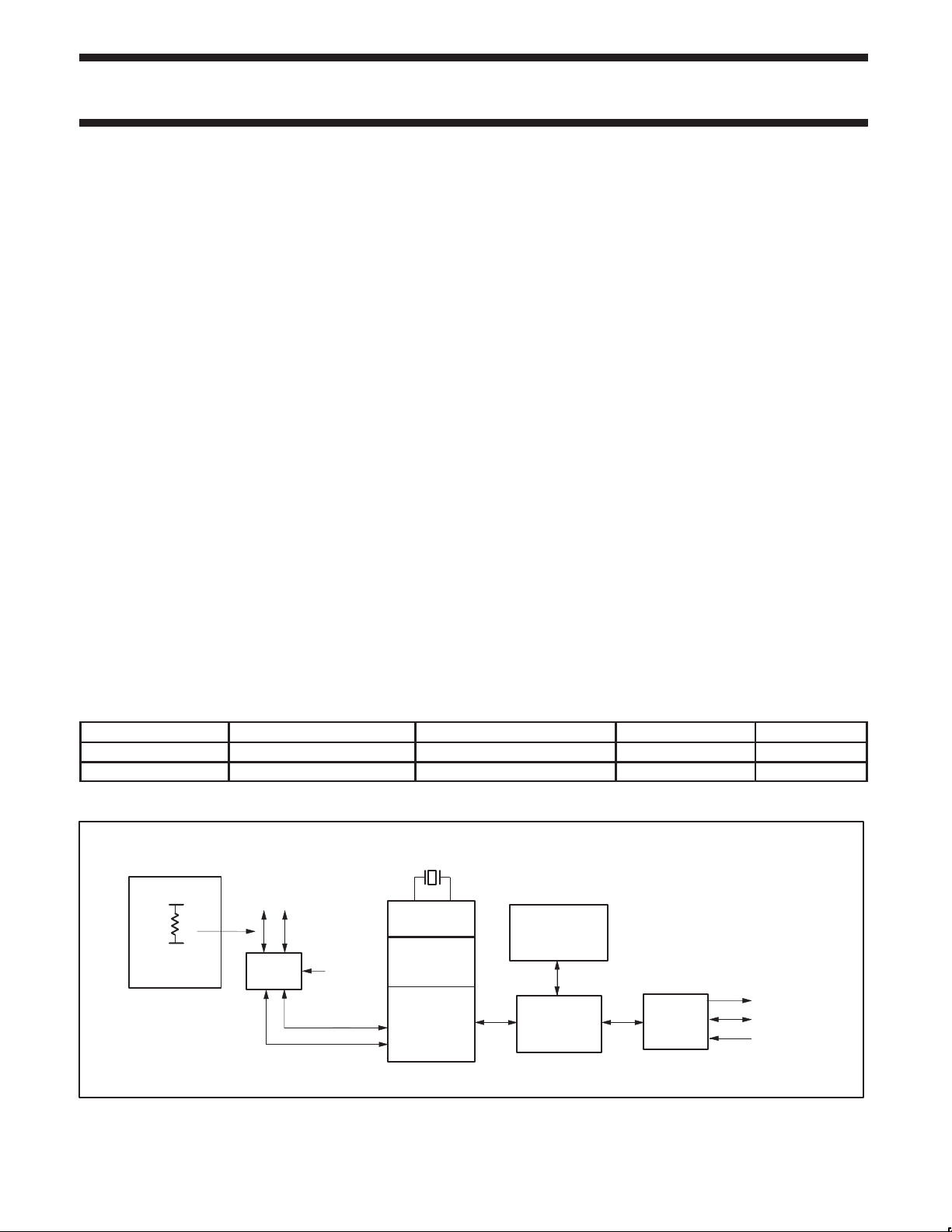
BLOCK DIAGRAM
12 MHz
UPSTREAM
3.3V
1.5kW
D+
SoftConnect
NOTE:
1. This is a conceptual block diagram and does not include each individual signal.
PORT
D+
ANALOG
TX/R
D–
FULL SPEED
X
PLL
BIT CLOCK
RECOVERY
PHILIPS
SIE
INTEGRATED
RAM
MEMORY
MANAGEMENT
UNIT
2
C
I
SLAVE
INTERFACE
INTERRUPT
SDA
SCL
SV00823
1999 Jul 22 853-2050 22023
2

Philips Semiconductors Product specification
03Control
1
Generic
2
Generic
3
Generic
PDIUSBD1 1USB device with serial interface
Analog Transceiver
The transceiver interfaces directly to the USB cables through some
termination resistors. They are capable of transmitting and receiving
serial data at “full speed” (12 Mbit/s) only.
PLL
A 12 MHz to 48 MHz clock multiplier PLL (Phase-Locked Loop) is
integrated on-chip. This allows for the use of low-cost 12 MHz
crystal. EMI is also minimized due to lower frequency crystal. No
external components are needed for the operation of the PLL.
Bit Clock Recovery
The bit clock recovery circuit recovers the clock from the incoming
USB data stream using 4X over-sampling principle. It is able to track
jitter and frequency drift specified by the USB specification.
Philips Serial Interface Engine (PSIE)
The Philips SIE implements the full USB protocol layer. It is
completely hardwired for speed and needs no firmware intervention.
The functions of this block include: synchronization pattern
recognition, parallel/serial conversion, bit stuffing/de-stuffing, CRC
checking/generation, PID verification/generation, address
recognition, handshake evaluation/generation.
Memory Management Unit (MMU) and Integrated RAM
The MMU and the integrated RAM is used to handle the large
difference in data rate between USB, running in bursts of 12 Mbit/s
and the I
This allows the microcontroller to read and write USB packets at its
own speed through I
2
C interface to the microcontroller, running at up to 1 Mbit/s.
2
C.
I2C Slave Interface
This block implements the necessary I2C interface protocol. A slave
2
I
C allows for simple micro-coding. An interrupt is used to alert the
microcontroller whenever the PDIUSBD1 1 needs attention. As a
2
slave I
C device, the PDIUSBD11 I2C clock: SCL is an input and is
controlled by the microcontroller. The I
1 Mbit/s.
2
C interface can run up to
SoftConnect
The connection to the USB is accomplished by bringing D+ (for
high-speed USB device) high through a 1.5 kW pull-up resistor. In
the PDIUSBD11, the 1.5 kW pull-up resistor is integrated on-chip
and is not connected to V
internal resistor to Vcc is established through a command sent by
the external/system microcontroller. This allows the system
microcontroller to complete its initialization sequence before
deciding to establish connection to the USB. Re-initialization of the
USB bus connection can also be affected without requiring the pull
out of the cable.
The PDIUSBD11 will check for USB VBUS availability before the
connection can be established. VBUS sensing is provided through
VBUS pin.
It should be noted that the tolerance of the internal resistors is
higher (30%) than that specified by the USB specification (5%).
However, the overall V
can still be met with good margin. The decision to make sure of this
feature lies with the users.
SoftConnect is a patent pending technology from Philips
Semiconductors.
by default. The connection of the
CC
voltage specification for the connection
SE
ENDPOINT DESCRIPTIONS
ENDPOINT# ENDPOINT INDEX TRANSFER TYPE DIRECTION
2
5
4
6
7
8
9
NOTE:
1. Generic endpoint can be used for Interrupt or Bulk endpoint.
MAX
PACKET SIZE
(BYTES)
OUT 8
IN 8
OUT 8
IN 8
OUT 8
IN 8
OUT 8
IN 8
1999 Jul 22
3
Philips Semiconductors Product specification
PDIUSBD1 1USB device with serial interface
PIN DESCRIPTION
PIN NO PIN SYMBOL TYPE DRIVE DESCRIPTION
1 TEST Input Connect to GND for normal operation
2 RESET_N Input ST Power-on reset
3 XTAL1 Input Crystal connection 1 (12MHz)
4 XTAL2 Output Crystal connection 2 (12MHz)
5 CLKOUT Output 3 mA Programmable output clock for external devices
6 V
CC
7 SUSPEND Output OD6 Device is in suspended state
8 INT_N Output OD6 Connect to microcontroller interrupt
9 SDA I/O OD6 I2C bi-directional data
10 SCL I/O OD6 I2C bit-clock
11 GND Power Ground reference
12 DP AI/O USB D+ connection
13 DM AI/O USB D– connection
14 AGND Power Analog ground reference
15 AV
CC
16 VBUS Input USB VBUS sensing pin
NOTES:
1. Signals ending in _N indicate active LOW signals.
ST: Schmitt Trigger
OD6: Open Drain with 6 mA drive
AI/O: Analog I/O
Power Voltage supply 3.3V±0.3V
Power Analog voltage supply 3.3V±0.3V
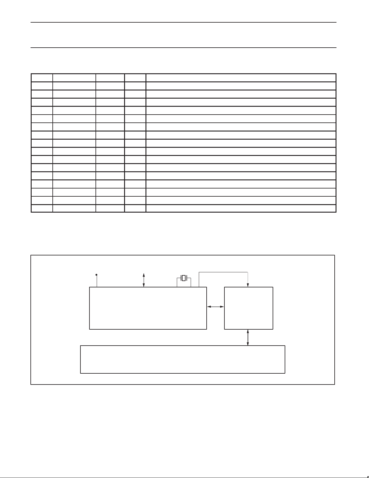
APPLICATION DIAGRAM
3.3V
USB Upstream
D11
e.g. Monitor Control, Mouse, Keyboard, ...
12 MHz
CLKOUT
I2C
µC
FUNCTIONAL BLOCK
SV00824
1999 Jul 22
4

Philips Semiconductors Product specification
PDIUSBD1 1USB device with serial interface
I2C Interface
The I2C bus is used to interface to an external microcontroller
needed to control the operation of the USB device. For cost
consideration, the target system microcontroller can be shared and
utilized for both the functional part as well as the USB protocol
interfacing. The PDIUSBD1 1 implements a slave I
When the PDIUSBD11 needs to communicate with the
microcontroller it asserts an interrupt signal. The microcontroller
services this interrupt by reading the appropriate status register on
the PDIUSBD11 through the I
2
the I
C serial bus, refer to the
9397 750 00013).
2
The I
C interface on the PDIUSBD11 defines two types of
transactions:
2
C bus. (For more information about
I2C Handbook
2
C interface.
, Philips order number
•command transaction – A command transaction is used to
define which data (e.g., status byte, buffer data, ...) will be read
from/written to the USB interface in the next data transaction. A
data transaction usually follows a command transaction.
•data transaction – A data transaction reads data from/writes
data to the USB interface. The meaning of the data is dependent
on the command transaction which was sent before the data
transaction.
Two addresses are used to differentiate between command and
data transactions. Writing to the command address is interpreted as
a command, while reading from/writing to the data address is used
to transfer data between the PDIUSBH11A and the controller.
Protocol
An I2C transaction starts with a Start Condition, followed by an
address. When the address matches either the command or data
address the transaction starts and runs until a Stop Condition or
another Start Condition (repeated start) occurs.
The command address is write-only and is unable to do a read. The
next bytes in the message are interpreted as commands. Several
command bytes can be sent after one command address. Each of
the command bytes is acknowledged and passed on to the Memory
Management Unit inside the PDIUSBD11.
When the Start Condition address matches the data address, the
next bytes are interpreted as data. When the RW bit in the address
indicates a
acknowledged and passed on to the Memory Management Unit. If
the RW bit in the address indicates a
(=‘1’) the PDIUSBD11 will send data to the master. The I2C-master
must acknowledge all data bytes except the last one. In this way the
I2C interface knows when the last byte has been transmitted and it
then releases the SDA line so that the master controller can
generate the Stop Condition.
Repeated start support allows another packet to be sent without
generating a Stop Condition.
master writes data to slave
(=‘0’) the bytes are received,
master reads data from slave
Timing
The I2C interface in the PDIUSBD11 can support clock speeds up to
1 MHz.
ADDRESS TABLE
Type of Address
Command 0011 011
Data 0011 010
Physical Address
MSB to LSB
(Binary)
1999 Jul 22
5

Philips Semiconductors Product specification
PDIUSBD1 1USB device with serial interface
COMMAND SUMMARY
Some commands have the same command code (e.g., Read Buffer and Write Buffer). In these cases, the direction of the Data Phase (read or
write) indicates which command is executed.
COMMAND NAME
Initialization Commands
Set Address/Enable Function D1h Write 1 byte
Set Endpoint Enable Function D8h Write 1 byte
Set Mode Function F3h Write 2 byte
Data Flow Commands
Read Interrupt Register F4h Read 2 bytes
Select Endpoint Control OUT Endpoint 00h Read 1 byte (optional)
Control IN Endpoint 01h Read 1 byte (optional)
Other Endpoints 00h+Endpoint Index Read 1 byte (optional)
Read Last Transaction Status Control OUT Endpoint 40h Read 1 byte
Control IN Endpoint 41h Read 1 byte
Other Endpoints 40h+Endpoint Index Read 1 byte
Read Endpoint Status Control OUT Endpoint 80h Read 1 byte
Control IN Endpoint 81h Read 1 byte
Other Endpoints 80h+Endpoint Index Read 1 byte
Read Buffer Selected Endpoint F0h Read n bytes
Write Buffer Selected Endpoint F0h Write n bytes
Set Endpoint Status Control OUT Endpoint 40h Write 1 byte
Set Endpoint Status Control IN Endpoint 41h Write 1 byte
Other Endpoints 40h+Endpoint Index Write 1 byte
Acknowledge Setup Selected Endpoint F1h None
Clear Buffer Selected Endpoint F2h None
Validate Buf fer Selected Endpoint FAh None
General Commands
Send Resume F6h None
Read Current Frame Number F5h Read 1 or 2 bytes
RECIPIENT CODING DATA PHASE
1999 Jul 22
6
 Loading...