

Philips PDI1394P Service Manual

PDI1394P11
3-Port physical layer interface
Preliminary specification 1996 Oct 16
INTEGRATED CIRCUITS
Philips Semiconductors Preliminary specification
PDI1394P113-Port physical layer interface
2
1996 Oct 16
FEATURES
•3 cable interface ports
•Supports 100Mb/s and 200Mb/s transfers
•Interfaces to any 1394 standard Link Layer Controller
•5V tolerant I/Os
•Single 3.3V supply voltage
DESCRIPTION
The Philips Semiconductors PDI1394P11 is an IEEE1394 compliant
Physical Layer interface. The PDI1394P11 provides an associated
Link Layer Controller with an electrical interface to the 1394 cable
environment. Additionally, the device manages bus initialization
and arbitration cycles, as well as transmission and reception of data
bits. The Link Layer Controller interface is compatible with both 3V
and 5V Link Controllers. While providing a maximum transmission
data rate of 200 Mb/s, the PDI1394P11 is compatible with current
100 Mb/s and future 400 Mb/s systems. The PDI1394P11 is
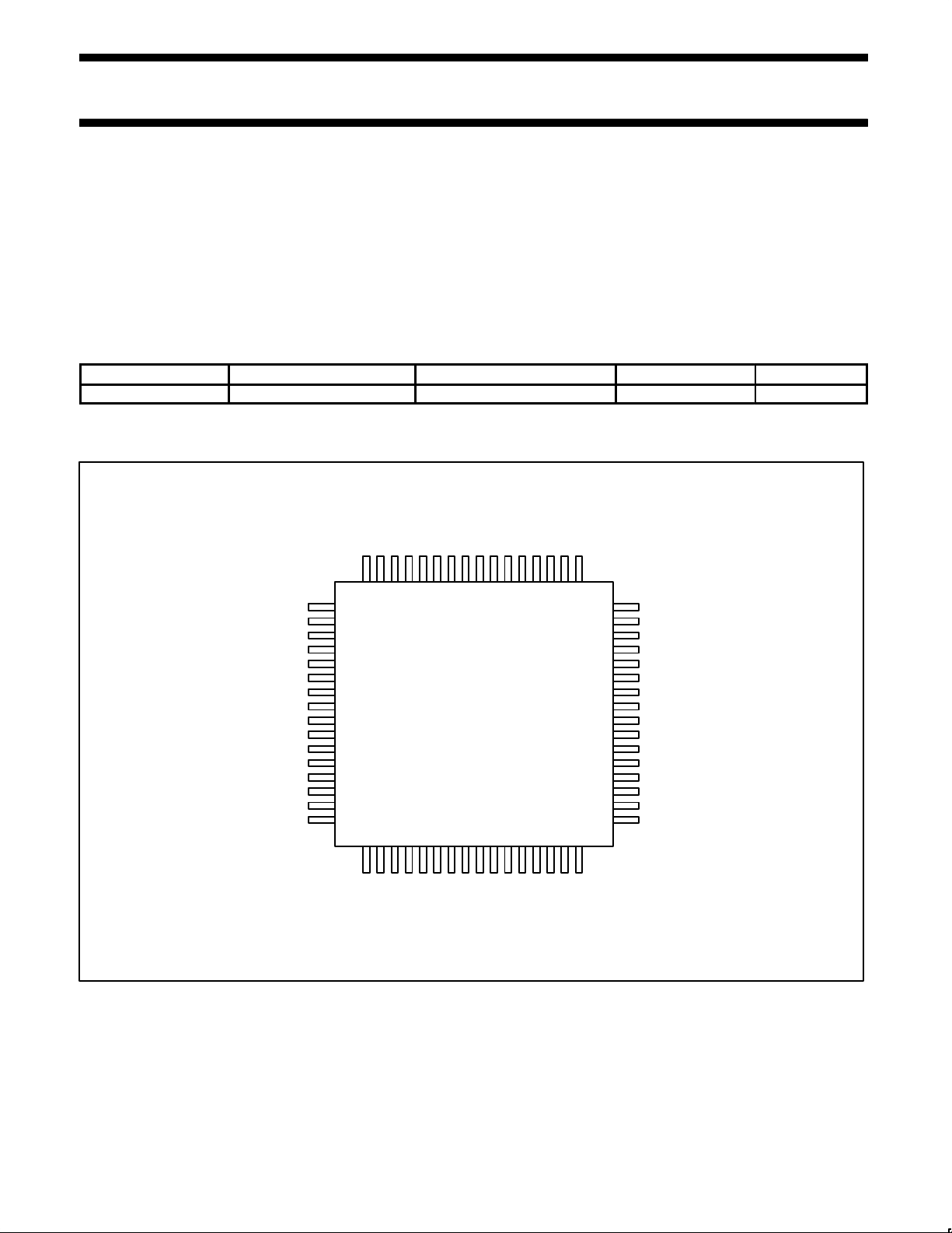
available in the LQFP64 package.
ORDERING INFORMATION
PACKAGE TEMPERATURE RANGE OUTSIDE NORTH AMERICA NORTH AMERICA PKG. DWG. #
64-pin plastic LQFP 0°C to +70°C PDI1394P11 PDI1394P11 SOT314-2
PIN CONFIGURATION
PDI1394P11
AGND AGND
AGND
AGND
AVDD
AVDD
AVDD
AVDD
AGND
PLLGND
PLLGND
PLLVDD
FILTER
X1
X0
R0
R1
ISO–_
DVSS
DVSS
CNA
PC2
PC1
PC0
CPS
TESTM1
TESTM2
DVDD
DVDD
DVSS
DVSS
CMC/LKON
TPBIAS2
AGND
TPBIAS1
TPBIAS3
TPA1–
TPB1+
TPA1+
TPB1–
TPA2–
TPB2+
TPA2+
TPB2–
TPA3–
TPB3+
TPA3+
TPB3–
LPS
RESERVED
LREQ
RESET–
DVDD
DVDD
DVDD
PD
DVSS
CTL0
SYSCLK
CTL1
D1
D2
D0
D3
31
30
32
29
27
26
28
25
23
22
24
21
19
18
20
17
50
51
49
52
54
55
53
56
58
59
57
60
62
63
61
64
47
46
48
45
43
42
44
41
39
38
40
37
353436
33
2
3
1
4
6
7
5
8
10
11
9
12
141513
16
SV00229

Philips Semiconductors Preliminary specification
PDI1394P113-Port physical layer interface
1996 Oct 16
3
PIN DESCRIPTION
PIN NUMBER PIN SYMBOL I/O NAME AND FUNCTION
1 /RESET I Power upreset, active LOW
2 LPS I Link power status
3 LREQ I Link request from controller
4 DVDD – Should be tied to 3.3V power supply
5, 6, 19, 20 DVCC – Digital circuit power
7 PD I Device power down input
8, 10, 17, 18, 63, 64 DGND – Digital circuit ground
9 SYSCLK O 49.152 clock to link controller
11, 12 CTL[0:1] I/O Link interface bi-directional control signals
13, 14, 15, 16 D[0:3] I/O Link interface bi-directional data signals
21, 22 TESTM[1:2] I Test mode control, normally tied high
23 CPS I Cable power status
24, 25, 51, 55 AVCC – Analog circuit power
26, 32, 41, 49, 50, 61 AGND – Analog circuit ground
27 CMC/LKON I/O Configuration Manager capable input, or LINK-ON signal output
28, 29, 30 PC[0:2] I Power class bits 2 through 0 inputs
31 CNA O Cable Not Active output
36, 40, 45 TPA[1:3]+ O Port n cable pair A, positive signal
35, 39, 44 TPA[1:3]– O Port n cable pair A, negative signal
34, 38, 43 TPA[1:3]+ O Port n cable pair B, positive signal
33, 37, 42 TPA[1:3]– O Port n cable pair B, negative signal
46, 47, 48 TPBIAS[1:3] O Cable termination voltage supplies
52, 53 PLLGND – PLL circuit ground
54 FILTER I/O PLL external filter capacitor
56, 57 X1,X0 – Crystal oscillator
58 PLLVCC – PLL circuit power
59, 60 R[0:1] – External current setting resistor, 6.8kΩ ±1.0%
62 /ISO I Link interface isolation status
Philips Semiconductors Preliminary specification
PDI1394P113-Port physical layer interface
1996 Oct 16
4
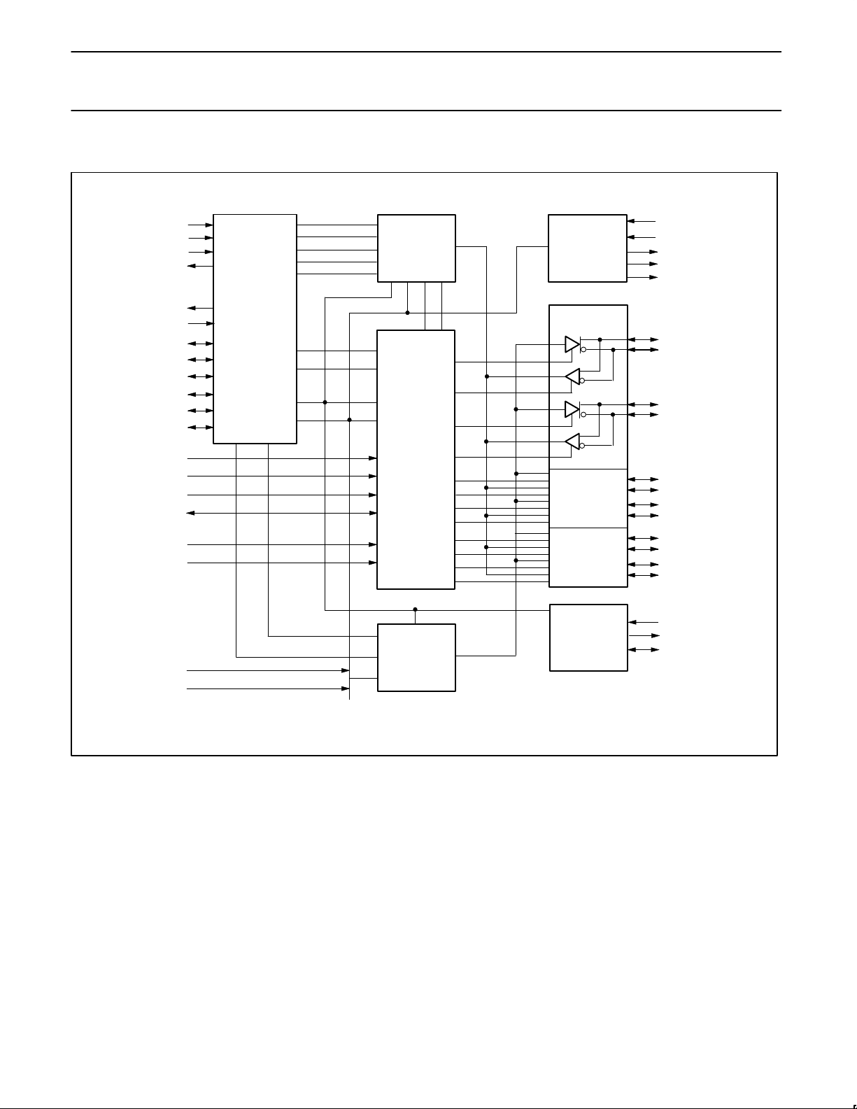
BLOCK DIAGRAM
PORT 1
PORT 2
PORT 3
BIAS
VOLTAGE AND
CURRENT
GENERATOR
RECEIVED
DATA
DECODER
/TIMER
LINK
INTERFACE
ARBITRATION
AND CONTROL
STATE
MACHINE
LOGIC
CRYSTAL
OSCILLATOR
PLL SYSTEM
& TRANSMIT
CLOCK
GENERATOR
TRANSMIT
DATA
ENCODER
TESTM1
TESTM2
C/LNKON
PC0
PC1
PC2
D0
D1
D2
D3
CTL0
CTL1
LREQ
SYSCLK
CNA
/ISO
LPS
CPS
/RESET
PWRDN
R0
R1
TPBIAS1
TPBIAS2
TPBIAS3
TPA1
/TPA1
TPB1
/TPB1
TPA2
/TPA2
TPB2
/TPB2
TPA3
/TPA3
TPB3
/TPB3
X1
X0
FILTER
SV00228

Philips Semiconductors Preliminary specification
PDI1394P113-Port physical layer interface
1996 Oct 16
5
FUNCTIONAL SPECIFICATION
Part 1
The PDI1394P11 is an IEEE1394–1995 High Performance Serial
Bus Specification compliant physical layer interface device. It
provides an analog interface between an attached link layer
controller and three1394 cable interface ports. In addition to the
analog interface function, the PDI1394P11 performs bus initialization
and arbitration functions as well as monitoring line conditions and
connection status.
Clocking
The PDI1394P11 utilizes a stable internal reference clock of
196.608 MHz. The reference clock is generated using an external
24.576 Mhz crystal and an internal Phased Lock Loop (PLL). The
PLL clock is divided down to 49.152 MHz and 98.304 MHz clock
signals. The 49.152 MHz clock is used for internal logic and
provided as an output to clock an associated link layer controller.
The 98.304MHz clock is used for synchronization of the transmitted
strobe and data information.
Analog Port Interfaces
The PDI1394P11 provides the analog transceiver functions needed
to implement a three port node in a cable–based 1394 network.
Each cable port incorporates two differential line transceivers. In
addition to transmission and reception of packet data, the line
transceivers monitor conditions on the cable to determine
connection status, data speed, and bus arbitration states.
The PDI1394P11 receives data to be transmitted over the bus from
two or four parallel data paths to the Link Controller, D[0:3]. These
data paths are latched and synchronized with the 49.152 MHz clock.
The parallel bit paths are combined serially, encoded and
transmitted at either 98.304 Mb/s or 196.608 Mb/s, depending
whether the transaction is a 100 Mb/s or 200 Mb/s transfer,
respectively. The transmitted data is encoded as data–strobe
information, with the data information being transmitted on the TPB
cable pairs and the strobe information appearing on the TPA cable
pairs.
During packet reception the TPA and TPB transmitters of the
receiving cable port are disabled, and the receivers for that port are
enabled. The encoded data information is received on the TPA
cable pair and the strobe information is received on the TPB cable
pair. The combination of the data and strobe signals is decoded to
recover the receive clock signal and the serial data stream. The
serial data stream is converted to two or four parallel data streams,
resynchronized to the internal 49.152 MHz clock and sent to the
associated link controller. The received data is also transmitted out
the other active cable ports.
The cable status and bus initialization and arbitration states are
monitored through the cable interface using differential comparators.
The outputs of these comparators are used by internal logic to
determine cable and arbitration status. The TPA channel monitors
the incoming cable common–mode voltage value during arbitration
to determine the speed of the next packet transmission. The TPB
channel monitors the incoming cable common–mode voltage for the
presence of the remotely supplied twisted–pair bias voltage,
indicating the cable connection status.
The PDI1394P11 provides a nominal 1.86 Volt for driver load
termination. This bias voltage, when seen through a cable by a
remote receiver, is used to sense the presence of an active
connection. The value of this bias voltage has been chosen to
allow inter–operability between transceiver chips operating from
either 5 volt nominal supplies, or 3 volt nominal supplies. This bias
voltage source should be stabilized by using an external filter
capacitor of approximately 1.0 µF.

Philips Semiconductors Preliminary specification
PDI1394P113-Port physical layer interface
1996 Oct 16
6
RECOMMENDED OPERATING CONDITIONS
LIMITS
SYMBOL
PARAMETER
CONDITION
UNIT
MIN.
MIN.
MAX.
V
CC
DC supply voltage 3.0
1
3.3 3.6 V
V
IH
High level input voltage CMOS inputs 0.7V
CC
V
V
IL
Low level input voltage CMOS inputs 142 0.2V
CC
V
V
ID–100
Differential input voltage Cable inputs, 100Mbit operation 132 260 mV
V
ID–200
Differential input voltage Cable inputs, 200Mbit operation 171 260 mV
V
ID–ARB
Differential input voltage Cable inputs, during arbitration 1.165 262 mV
VCM–100 Common mode voltage TPB cable inputs, 100Mbit or speed signaling OFF 0.935 2.515
3
V
VCM–200SP Common mode voltage TPB cable inputs, 200Mbit or speed signaling 2.515
3
V
Receive input jitter TPA, TPB cable inputs, 100Mbit operation ±1.08 ns
Receive input skew Between TPA and TPB cable inputs, 100Mbit operation ±0.8 ns
Receive input jitter TPA, TPB cable inputs, 200Mbit operation ±0.5 ns
Receive input skew Between TPA and TPB cable inputs, 200Mbit operation ±0.55 ns
IOL/I
OH
Output current SYSCLK Control, Data, CNA and CMC/LKON outputs
–16
–12
16
12
mA
I
O
Output current TPBIAS outputs –3 1.3 mA
NOTES:
1. A minimum V
CC
of 2.7V may be used when this device is used in a single port end-of-wire power consuming application only.
2. A maximum of 2.015V applies for supply voltages less than 3.0V electrical characteristics over recommended ranges of operating conditions
(unless otherwise noted).
3. Limits defined as algebraic average of TPA+ and TPA– common mode currents. Limits also apply to TPB+ and TPB– algebraic average
common mode currents.
ABSOLUTE MAXIMUM RATINGS
1
In accordance with the Absolute Maximum Rating System (IEC 134) Voltages are referenced to GND (ground = 0V)
LIMITS
SYMBOL
PARAMETER
CONDITION
MIN TYP MAX
UNIT
V
CC
DC supply voltage –0.3 4.0 V
V
I
DC input voltage –0.5 V
CC
+0.5 V
V
O
DC output voltage –0.5 VCC +0.5 V
T
amb
Operating ambient temperature range in free
air
0 0 +70 °C
T
stg
Storage temperature range –65 +150 °C
NOTES:
1. Stresses beyond those listed may cause permanent damage to the device. These are stress ratings only and functional operation of the
device at these or any other conditions beyond those indicated under “recommended operating conditions” is not implied. Exposure to
absolute-maximum-rated conditions for extended periods may affect device reliability.
2. The performance capability of a high-performance integrated circuit in conjunction with its thermal environment can create junction
temperatures which are detrimental to reliability. The maximum junction temperature of this integrated circuit should not exceed 150°C.
3. The input and output voltage ratings may be exceeded if the input and output clamp current ratings are observed.
 Loading...