

Philips PDI1394L41 Datasheet

INTEGRATED CIRCUITS
PDI1394L41
1394 content protection AV link layer
controller
Preliminary specification
Supersedes data of 1999 Sep 30
NOTICE: DTLA SENSITIVE INFORMATION HAS BEEN WITHHELD FROM THIS DATA SHEET. SEE SECTION 2.1 FOR DETAILS.
2000 Apr 15

Philips Semiconductors Preliminary specification
PDI1394L411394 content protection AV link layer controller
1.0 FEATURES 1. . . . . . . . . . . . . . . . . . . . . . . . . . . . . . . . . . . . . . . . . . . . . . . . . . . . . . . . . . . . . . . . . . . . . . . . . . . . . . . . . . . . . . . . .
2.0 DESCRIPTION 1. . . . . . . . . . . . . . . . . . . . . . . . . . . . . . . . . . . . . . . . . . . . . . . . . . . . . . . . . . . . . . . . . . . . . . . . . . . . . . . . . . . . . .
3.0 QUICK REFERENCE DATA 1. . . . . . . . . . . . . . . . . . . . . . . . . . . . . . . . . . . . . . . . . . . . . . . . . . . . . . . . . . . . . . . . . . . . . . . . . .
4.0 ORDERING INFORMATION 1. . . . . . . . . . . . . . . . . . . . . . . . . . . . . . . . . . . . . . . . . . . . . . . . . . . . . . . . . . . . . . . . . . . . . . . . . .
5.0 PIN CONFIGURATION 2. . . . . . . . . . . . . . . . . . . . . . . . . . . . . . . . . . . . . . . . . . . . . . . . . . . . . . . . . . . . . . . . . . . . . . . . . . . . . . .
6.0 FUNCTIONAL DIAGRAM 3. . . . . . . . . . . . . . . . . . . . . . . . . . . . . . . . . . . . . . . . . . . . . . . . . . . . . . . . . . . . . . . . . . . . . . . . . . . .
7.0 INTERNAL BLOCK DIAGRAM 3. . . . . . . . . . . . . . . . . . . . . . . . . . . . . . . . . . . . . . . . . . . . . . . . . . . . . . . . . . . . . . . . . . . . . . . .
8.0 APPLICATION DIAGRAM 4. . . . . . . . . . . . . . . . . . . . . . . . . . . . . . . . . . . . . . . . . . . . . . . . . . . . . . . . . . . . . . . . . . . . . . . . . . . .
9.0 PIN DESCRIPTION 4. . . . . . . . . . . . . . . . . . . . . . . . . . . . . . . . . . . . . . . . . . . . . . . . . . . . . . . . . . . . . . . . . . . . . . . . . . . . . . . . . .
9.1 Host Interface 4. . . . . . . . . . . . . . . . . . . . . . . . . . . . . . . . . . . . . . . . . . . . . . . . . . . . . . . . . . . . . . . . . . . . . . . . . . . . . . . . . . . .
9.2 A V Interface 1 5. . . . . . . . . . . . . . . . . . . . . . . . . . . . . . . . . . . . . . . . . . . . . . . . . . . . . . . . . . . . . . . . . . . . . . . . . . . . . . . . . . . .
9.3 A V Interface 2 6. . . . . . . . . . . . . . . . . . . . . . . . . . . . . . . . . . . . . . . . . . . . . . . . . . . . . . . . . . . . . . . . . . . . . . . . . . . . . . . . . . . .
9.4 Phy Interface 7. . . . . . . . . . . . . . . . . . . . . . . . . . . . . . . . . . . . . . . . . . . . . . . . . . . . . . . . . . . . . . . . . . . . . . . . . . . . . . . . . . . . .
9.5 Other Pins 7. . . . . . . . . . . . . . . . . . . . . . . . . . . . . . . . . . . . . . . . . . . . . . . . . . . . . . . . . . . . . . . . . . . . . . . . . . . . . . . . . . . . . . .
10.0 RECOMMENDED OPERATING CONDITIONS 8. . . . . . . . . . . . . . . . . . . . . . . . . . . . . . . . . . . . . . . . . . . . . . . . . . . . . . . . .
11.0 ABSOLUTE MAXIMUM RATINGS 8. . . . . . . . . . . . . . . . . . . . . . . . . . . . . . . . . . . . . . . . . . . . . . . . . . . . . . . . . . . . . . . . . . . .
12.0 FUNCTIONAL DESCRIPTION 9. . . . . . . . . . . . . . . . . . . . . . . . . . . . . . . . . . . . . . . . . . . . . . . . . . . . . . . . . . . . . . . . . . . . . . .
12.1 Overview 9. . . . . . . . . . . . . . . . . . . . . . . . . . . . . . . . . . . . . . . . . . . . . . . . . . . . . . . . . . . . . . . . . . . . . . . . . . . . . . . . . . . . . . .
12.2 A V interface and AV layer 9. . . . . . . . . . . . . . . . . . . . . . . . . . . . . . . . . . . . . . . . . . . . . . . . . . . . . . . . . . . . . . . . . . . . . . . . .
12.2.1 IEC 61883 International Standard 9. . . . . . . . . . . . . . . . . . . . . . . . . . . . . . . . . . . . . . . . . . . . . . . . . . . . . . . . . . . . . .
12.2.2 CIP Headers 9. . . . . . . . . . . . . . . . . . . . . . . . . . . . . . . . . . . . . . . . . . . . . . . . . . . . . . . . . . . . . . . . . . . . . . . . . . . . . . . .
12.2.3 The AV Interface 9. . . . . . . . . . . . . . . . . . . . . . . . . . . . . . . . . . . . . . . . . . . . . . . . . . . . . . . . . . . . . . . . . . . . . . . . . . . . .
12.2.4 Content Protection 10. . . . . . . . . . . . . . . . . . . . . . . . . . . . . . . . . . . . . . . . . . . . . . . . . . . . . . . . . . . . . . . . . . . . . . . . . . .
12.2.5 mLAN Support 11. . . . . . . . . . . . . . . . . . . . . . . . . . . . . . . . . . . . . . . . . . . . . . . . . . . . . . . . . . . . . . . . . . . . . . . . . . . . . .
12.2.6 SY – Sync Support 11. . . . . . . . . . . . . . . . . . . . . . . . . . . . . . . . . . . . . . . . . . . . . . . . . . . . . . . . . . . . . . . . . . . . . . . . . .
12.2.7 Programmable Buffer Memory 11. . . . . . . . . . . . . . . . . . . . . . . . . . . . . . . . . . . . . . . . . . . . . . . . . . . . . . . . . . . . . . . . .
12.3 Bushold and Link/PHY single capacitor galvanic isolation 12. . . . . . . . . . . . . . . . . . . . . . . . . . . . . . . . . . . . . . . . . . . . . .
12.3.1 Bushold 12. . . . . . . . . . . . . . . . . . . . . . . . . . . . . . . . . . . . . . . . . . . . . . . . . . . . . . . . . . . . . . . . . . . . . . . . . . . . . . . . . . . .
12.3.2 Single capacitor isolation 13. . . . . . . . . . . . . . . . . . . . . . . . . . . . . . . . . . . . . . . . . . . . . . . . . . . . . . . . . . . . . . . . . . . . .
12.4 Power Management 13. . . . . . . . . . . . . . . . . . . . . . . . . . . . . . . . . . . . . . . . . . . . . . . . . . . . . . . . . . . . . . . . . . . . . . . . . . . . . .
12.5 The host interface 14. . . . . . . . . . . . . . . . . . . . . . . . . . . . . . . . . . . . . . . . . . . . . . . . . . . . . . . . . . . . . . . . . . . . . . . . . . . . . . . .
12.5.1 Read accesses 14. . . . . . . . . . . . . . . . . . . . . . . . . . . . . . . . . . . . . . . . . . . . . . . . . . . . . . . . . . . . . . . . . . . . . . . . . . . . . .
12.5.2 Write accesses 15. . . . . . . . . . . . . . . . . . . . . . . . . . . . . . . . . . . . . . . . . . . . . . . . . . . . . . . . . . . . . . . . . . . . . . . . . . . . . .
12.5.3 Big and little endianness, data invariance, and data bus width 16. . . . . . . . . . . . . . . . . . . . . . . . . . . . . . . . . . . . .
12.5.4 Accessing the asynchronous packet queues 17. . . . . . . . . . . . . . . . . . . . . . . . . . . . . . . . . . . . . . . . . . . . . . . . . . . .
12.5.5 The CPU bus interface signals 18. . . . . . . . . . . . . . . . . . . . . . . . . . . . . . . . . . . . . . . . . . . . . . . . . . . . . . . . . . . . . . . .
12.6 The Asynchronous Packet Interface 26. . . . . . . . . . . . . . . . . . . . . . . . . . . . . . . . . . . . . . . . . . . . . . . . . . . . . . . . . . . . . . . .
12.6.1 Reading an Asynchronous Packet 26. . . . . . . . . . . . . . . . . . . . . . . . . . . . . . . . . . . . . . . . . . . . . . . . . . . . . . . . . . . . .
12.6.2 Link Packet Data Formats 26. . . . . . . . . . . . . . . . . . . . . . . . . . . . . . . . . . . . . . . . . . . . . . . . . . . . . . . . . . . . . . . . . . . .
12.7 Interrupts 40. . . . . . . . . . . . . . . . . . . . . . . . . . . . . . . . . . . . . . . . . . . . . . . . . . . . . . . . . . . . . . . . . . . . . . . . . . . . . . . . . . . . . . .
13.0 REGISTER MAP 41. . . . . . . . . . . . . . . . . . . . . . . . . . . . . . . . . . . . . . . . . . . . . . . . . . . . . . . . . . . . . . . . . . . . . . . . . . . . . . . . . . .
13.1 Link Control Registers 46. . . . . . . . . . . . . . . . . . . . . . . . . . . . . . . . . . . . . . . . . . . . . . . . . . . . . . . . . . . . . . . . . . . . . . . . . . . .
13.1.1 ID Register (IDREG) – Base Address: 0x000 46. . . . . . . . . . . . . . . . . . . . . . . . . . . . . . . . . . . . . . . . . . . . . . . . . . . .
13.1.2 General Link Control (LNKCTL) – Base Address: 0x004 46. . . . . . . . . . . . . . . . . . . . . . . . . . . . . . . . . . . . . . . . . .
13.1.3 Link /Phy Interrupt Acknowledge (LNKPHYINTACK) – Base Address: 0x008 48. . . . . . . . . . . . . . . . . . . . . . . . .
13.1.4 Link / Phy Interrupt Enable (LNKPHYINTE) – Base Address: 0x00C 49. . . . . . . . . . . . . . . . . . . . . . . . . . . . . . . .
13.1.5 Cycle Timer Register (CYCTM) – Base Address: 0x010 49. . . . . . . . . . . . . . . . . . . . . . . . . . . . . . . . . . . . . . . . . . .
13.1.6 Phy Register Access (PHYACS) – Base Address: 0x014 50. . . . . . . . . . . . . . . . . . . . . . . . . . . . . . . . . . . . . . . . . .
13.1.7 Global Interrupt Status and TX Control (GLOBCSR) – Base Address: 0x018 50. . . . . . . . . . . . . . . . . . . . . . . . .
13.1.8 Timer (TIMER) – Base Address: 0x01C 51. . . . . . . . . . . . . . . . . . . . . . . . . . . . . . . . . . . . . . . . . . . . . . . . . . . . . . . . .
13.2 AV (Isochronous) Transmitter and Receiver Registers 52. . . . . . . . . . . . . . . . . . . . . . . . . . . . . . . . . . . . . . . . . . . . . . . . .
13.2.1 Isochronous Transmit Packing Control and Status (ITXPKCTL) – Base Address: 0x020 52. . . . . . . . . . . . . . .
13.2.2 Common Isochronous Transmit Packet Header Quadlet 1 (ITXHQ1) – Base Address: 0x024 53. . . . . . . . . . .
13.2.3 Common Isochronous Transmit Packet Header Quadlet 2 (ITXHQ2) – Base Address: 0x028 53. . . . . . . . . . .
2000 Apr 15
i

Philips Semiconductors Preliminary specification
PDI1394L411394 content protection AV link layer controller
13.2.4 Isochronous Transmitter Interrupt Acknowledge (ITXINTACK) – Base Address: 0x02C 54. . . . . . . . . . . . . . . .
13.2.5 Isochronous Transmitter Interrupt Enable (ITXINTE) – Base Address: 0x030 54. . . . . . . . . . . . . . . . . . . . . . . . .
13.2.6 Isochronous Transmitter Control Register (ITXCTL) – Base Address: 0x34 55. . . . . . . . . . . . . . . . . . . . . . . . . .
13.2.7 Isochronous Transmitter Memory Status (ITXMEM) – Base Address: 0x038 55. . . . . . . . . . . . . . . . . . . . . . . . .
13.2.8 Isochronous Receiver Unpacking Control (IRXPKCTL) – Base Address: 0x040 56. . . . . . . . . . . . . . . . . . . . . .
13.2.9 Common Isochronous Receiver Packet Header Quadlet 1 (IRXHQ1) – Base Address: 0x044 57. . . . . . . . . .
13.2.10 Common Isochronous Receiver Packet Header Quadlet 2 (IRXHQ2) – Base Address: 0x048 57. . . . . . . . .
13.2.11 Isochronous Receiver Interrupt Acknowledge (IRXINTACK) – Base Address: 0x04C 58. . . . . . . . . . . . . . . . .
13.2.12 Isochronous Receiver Interrupt Enable (IRXINTE) – Base Address: 0x050 58. . . . . . . . . . . . . . . . . . . . . . . . .
13.2.13 Isochronous Receiver Control Register (IRXCTL) – Base Address: 0x054 59. . . . . . . . . . . . . . . . . . . . . . . . . .
13.2.14 Isochronous Receiver Memory Status (IRXMEM) – Base Address: 0x058 60. . . . . . . . . . . . . . . . . . . . . . . . . .
13.3 Asynchronous Control and Status Interface 61. . . . . . . . . . . . . . . . . . . . . . . . . . . . . . . . . . . . . . . . . . . . . . . . . . . . . . . . . .
13.3.1 Asynchronous RX/TX Control (ASYCTL) – Base Address: 0x080 61. . . . . . . . . . . . . . . . . . . . . . . . . . . . . . . . . . .
13.3.2 Asynchronous RX/TX Memory Status (ASYMEM) – Base Address: 0x084 61. . . . . . . . . . . . . . . . . . . . . . . . . . .
13.3.3 Asynchronous Transmit Request Next (TX_RQ_NEXT) – Base Address: 0x088 62. . . . . . . . . . . . . . . . . . . . . .
13.3.4 Asynchronous Transmit Request Last (TX_RQ_LAST) – Base Address: 0x08C 62. . . . . . . . . . . . . . . . . . . . . .
13.3.5 Asynchronous Transmit Response Next (TX_RP_NEXT) – Base Address: 0x090 62. . . . . . . . . . . . . . . . . . . . .
13.3.6 Asynchronous Transmit Response Last (TX_RP_LAST) – Base Address: 0x094 62. . . . . . . . . . . . . . . . . . . . .
13.3.7 Asynchronous Receive Request (RREQ) – Base Address: 0x098 63. . . . . . . . . . . . . . . . . . . . . . . . . . . . . . . . . .
13.3.8 Asynchronous Receive Response (RRSP) – Base Address: 0x09C 63. . . . . . . . . . . . . . . . . . . . . . . . . . . . . . . . .
13.3.9 Asynchronous RX/TX Interrupt Acknowledge (ASYINTACK) – Base Address: 0x0A0 63. . . . . . . . . . . . . . . . . .
13.3.10 Asynchronous RX/TX Interrupt Enable (ASYINTE) – Base Address: 0x0A4 64. . . . . . . . . . . . . . . . . . . . . . . . .
13.3.11 RDI Register – Base Address: 0x0B0 64. . . . . . . . . . . . . . . . . . . . . . . . . . . . . . . . . . . . . . . . . . . . . . . . . . . . . . . . . .
13.3.12 Shadow Register (SHADOW_REG) – Base Address: 0x0F4 65. . . . . . . . . . . . . . . . . . . . . . . . . . . . . . . . . . . . . .
13.4 Indirect Address Registers 66. . . . . . . . . . . . . . . . . . . . . . . . . . . . . . . . . . . . . . . . . . . . . . . . . . . . . . . . . . . . . . . . . . . . . . . .
13.4.1 66. . . . . . . . . . . . . . . . . . . . . . . . . . . . . . . . . . . . . . . . . . . . . . . . . . . . . . . . . . . . . . . . . . . . . . . . . . . . . . . . . . . . . . . . . . .
13.4.2 Indirect Address Register (INDADDR) – Base Address: 0x0F8 66. . . . . . . . . . . . . . . . . . . . . . . . . . . . . . . . . . . . .
13.4.3 Indirect Data Register (INDDATA) – Base Address: 0x0FC 66. . . . . . . . . . . . . . . . . . . . . . . . . . . . . . . . . . . . . . . .
13.5 Indirect Address Registers 67. . . . . . . . . . . . . . . . . . . . . . . . . . . . . . . . . . . . . . . . . . . . . . . . . . . . . . . . . . . . . . . . . . . . . . . .
13.5.1 Registers for FIFO Size Programming 67. . . . . . . . . . . . . . . . . . . . . . . . . . . . . . . . . . . . . . . . . . . . . . . . . . . . . . . . . .
14.0 DC ELECTRICAL CHARACTERISTICS 70. . . . . . . . . . . . . . . . . . . . . . . . . . . . . . . . . . . . . . . . . . . . . . . . . . . . . . . . . . . . . . .
14.1 Pin Categories 70. . . . . . . . . . . . . . . . . . . . . . . . . . . . . . . . . . . . . . . . . . . . . . . . . . . . . . . . . . . . . . . . . . . . . . . . . . . . . . . . . . .
15.0 AC CHARACTERISTICS 71. . . . . . . . . . . . . . . . . . . . . . . . . . . . . . . . . . . . . . . . . . . . . . . . . . . . . . . . . . . . . . . . . . . . . . . . . . . .
16.0 TIMING DIAGRAMS 72. . . . . . . . . . . . . . . . . . . . . . . . . . . . . . . . . . . . . . . . . . . . . . . . . . . . . . . . . . . . . . . . . . . . . . . . . . . . . . . .
16.1 A V Interface Operation 72. . . . . . . . . . . . . . . . . . . . . . . . . . . . . . . . . . . . . . . . . . . . . . . . . . . . . . . . . . . . . . . . . . . . . . . . . . . .
16.2 A V Interface Critical Timings 72. . . . . . . . . . . . . . . . . . . . . . . . . . . . . . . . . . . . . . . . . . . . . . . . . . . . . . . . . . . . . . . . . . . . . . .
16.3 PHY-Link Interface Critical Timings 73. . . . . . . . . . . . . . . . . . . . . . . . . . . . . . . . . . . . . . . . . . . . . . . . . . . . . . . . . . . . . . . . .
16.4 Host Interface Critical Timings 74. . . . . . . . . . . . . . . . . . . . . . . . . . . . . . . . . . . . . . . . . . . . . . . . . . . . . . . . . . . . . . . . . . . . .
16.5 CYCLEIN/CYCLEOUT Timings 74. . . . . . . . . . . . . . . . . . . . . . . . . . . . . . . . . . . . . . . . . . . . . . . . . . . . . . . . . . . . . . . . . . . .
16.6 RESET Timings 75. . . . . . . . . . . . . . . . . . . . . . . . . . . . . . . . . . . . . . . . . . . . . . . . . . . . . . . . . . . . . . . . . . . . . . . . . . . . . . . . .
2000 Apr 15
ii

Philips Semiconductors Preliminary specification
PDI1394L411394 content protection AV link layer controller
1.0 FEATURES
•IEEE1394.a and IEEE1394–1995 Standard Link Layer Controller
•Hardware Support for the IEC61883 International Standard of
Digital Interface for Consumer Electronics
•Interface to any IEEE 1394–1995 or 1394.a Physical Layer
Interface
•5V Tolerant I/Os
•Single 3.3V supply voltage
•Full-duplex isochronous operation
•Operates with 400/200/100 Mbps physical layer devices
•12K byte fully programmable FIFO pool for isochronous and
asynchronous data
•Supports single capacitor isolation mode and IEEE 1394–1995,
Annex J. isolation
•6-field deep SYT buffer added to enhance real-time isochronous
synchronization using the AVFSYNC pin
•Generates its own AV port clocks under software control. Select
one of three frequencies: 24.576, 12.288, or 6.144 MHz
•Hardware support for the “5C” content protection method
•On chip timer resources
•Flexible 8/16 bit multiplexed/non-multiplexed host interface
•Parallel AV interface
•Fast 56-bit M6 cipher/decipher blocks capable of operating at over
80 Mbps
•Hardware authentication acceleration to reduce software
processor loading
•Highly configurable 12 K byte FIFO
2.0 DESCRIPTION
The PDI1394L41, Philips Semiconductors Full Duplex 1394
Audio/Video (AV) Link Layer Controller, is an IEEE 1394–1995
compliant link layer controller featuring 2 embedded AV layer
interfaces. The AV layers are designed to encrypt and pack, or
unpack and decrypt application data packets for transmission over
the IEEE1394 bus using isochronous data transfers and the “5C”
content protection method.
The application data is packetized according to the IEC 61883
International Standard of Interface for Consumer Electronic
Audio/Video Equipment. Both AV layer interfaces are byte-wide
ports capable of accommodating various MPEG–2 and DVC
codecs. A flexible host interface is provided for internal register
configuration as well as performing asynchronous data transfers.
Both 8 bit and 16 bit wide data paths, as well as
multiplexed/non-multiplexed access modes are supported.
The PDI1394L41 is powered by a single 3.3V power supply and the
inputs and outputs are 5V tolerant. It is available in the LQFP144
package.
2.1 Use restrictions
Due to rules set forth by the Digital Transmission Licensing
Administrator (DTLA) information concerning some features of the
L41 is the subject of a license issued by the DTLA. That information
has been omitted from this data sheet and is available only to DTLA
licensees on a restricted distribution basis. In order to obtain a copy
of the information, licensed parties should contact Philips
Semiconductors at 1394@philips.com and request data sheet
addendum AL41-1. Upon verification of the requestor’s DTLA
license status, a paper copy of the addendum will be sent to the
DTLA listed responsible person within the requesting company.
Distribution of samples and sales of the L41 chip are likewise
restricted to DTLA licensees. For information pertaining to the
procurement of a DTLA license please consult the DTLA website at
DTCP.com.
3.0 QUICK REFERENCE DATA
GND = 0V; T
SYMBOL
V
DD
I
DD
SCLK Device clock 49.147 49.152 49.157 MHz
= 25°C
amb
PARAMETER CONDITIONS MIN TYP MAX UNIT
Functional supply voltage range 3.0 3.3 3.6 V
Supply current @ VDD = 3.3V Operating 110 150 mA
4.0 ORDERING INFORMATION
PACKAGES TEMPERATURE RANGE OUTSIDE NORTH AMERICA NORTH AMERICA PKG. DWG. #
144-pin LQFP144 0°C to +70°C PDI1394L41BE PDI1394L41BE SOT486–1
NOTE:
This datasheet is subject to change.
Please visit out internet website www.semiconductors.philips.com/1394 for latest changes.
2000 Apr 15
1
Philips Semiconductors Preliminary specification
PDI1394L411394 content protection AV link layer controller
5.0 PIN CONFIGURATION
Pin Function
1 HIF D15
2 HIF D14
3 HIF D13
4 HIF D12
5 GND
6V
DD
7 HIF D11
8 HIF D10
9 HIF D9
10 HIF D8
11 GND
12 V
DD
13 HIF AD7
14 HIF AD6
15 HIF AD5
16 HIF AD4
17 GND
18 V
DD
19 HIF AD3
20 HIF AD2
21 HIF AD1
22 HIF AD0
23 GND
24 V
DD
25 HIF A8
26 HIF A7
27 HIF A6
28 HIF A5
29 HIF A4
30 HIF A3
31 HIF A2
32 HIF A1
33 HIF A0
34 GND
35 V
DD
36 HIF CSN
1
36
Pin Function
37 HIF WRN
38 HIF INTN
39 HIF ALE
40 HIF RDN
41 HIF WAIT
42 RESETN
43 GND
44 V
DD
45 HIF 16BIT
46 HIF MUX
47 1394 MODE
48 PD
49 RESERVED
50 RESERVED
51 RESERVED
52 RESERVED
53 GND
54 V
DD
55 CLK50
56 CYCLEIN
57 CYCLEOUT
58 RESERVED
59 RESERVED
60 GND
61 V
DD
62 TESTPIN
63 TESTPIN
64 TESTPIN
65 RESERVED
66 RESERVED
67 RESERVED
68 RESERVED
69 GND
70 V
DD
71 RESERVED
72 RESERVED
144
37
LQFP
109
108
73
72
Pin Function
73 PHY D7*
74 PHY D6*
75 PHY D5*
76 PHY D4*
77 GND
78 V
DD
79 PHY D3*
80 PHY D2*
81 PHY D1*
82 PHY D0*
83 GND
84 V
DD
85 PHY CTL1*
86 PHY CTL0*
87 LREQ
88 SCLK*
89 GND
90 V
DD
91 LPS*
92 LINKON
93 ISON
94 GND
95 V
DD
96 AV1ERR0
97 AV1ERR1
98 AV1ENDPCK
99 AV1CLK
100 AV1FSYNC
101 AV1 SY
102 AV1VALID
103 AV1SYNC
104 AV1EMIO
105 AV1EMI1
106 GND
107 V
DD
108 AV1D0
Pin Function
109 AV1D1
110 AV1D2
111 AV1D3
112 GND
113 V
DD
114 AV1D4
115 AV1D5
116 AV1D6
117 AV1D7
118 AV1READY
119 GND
120 V
DD
121 AV2ERR0/LTLEND
122 AV2ERR1/DATINV
123 AV2ENDPCK
124 AV2CLK
125 AV2FSYNC
126 AV2 SY
127 AV2VALID
128 AV2SYNC
129 AV2EMI0
130 AV2EMI1
131 GND
132 V
DD
133 AV2D0
134 AV2D1
135 AV2D2
136 AV2D3
137 GND
138 V
DD
139 AV2D4
140 AV2D5
141 AV2D6
142 AV2D7
143 AV2READY
144 RESERVED
2000 Apr 15
* Indicates pin equipped with internal bus hold circuit activated by the state of the ISON pin.
SV01020
2
Philips Semiconductors Preliminary specification
PDI1394L411394 content protection AV link layer controller
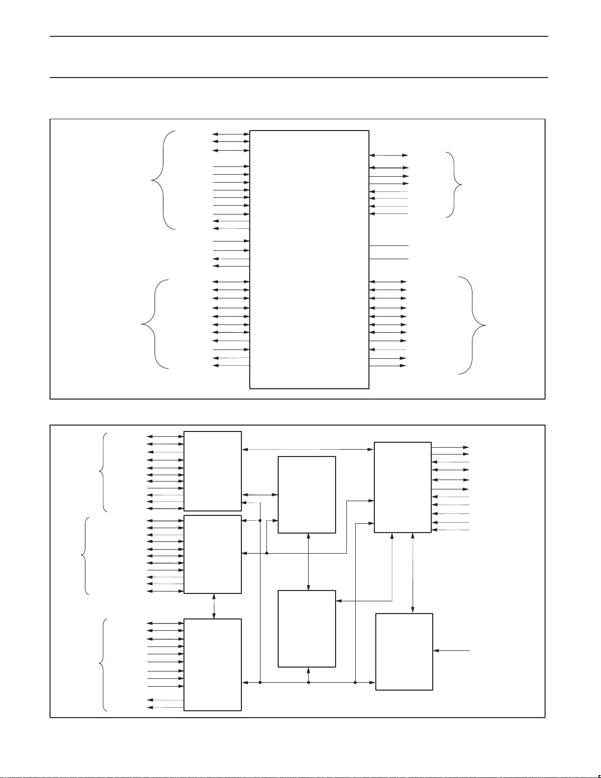
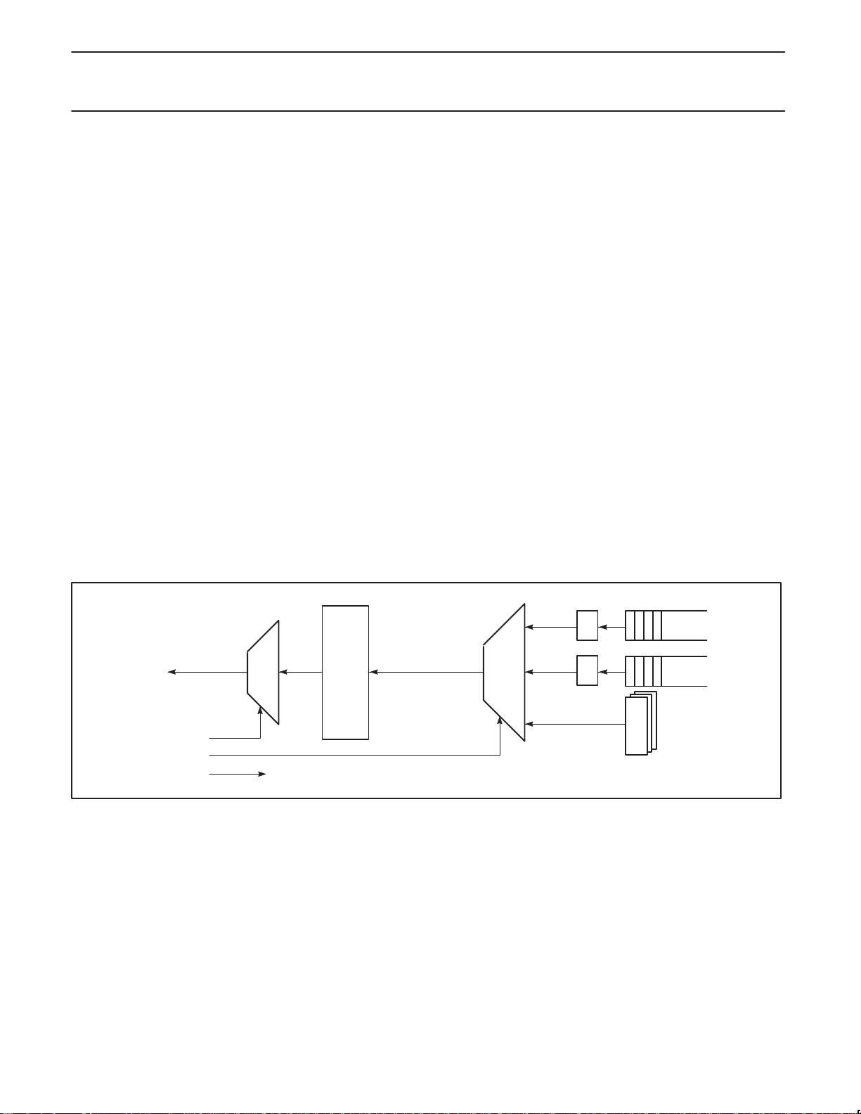
6.0 FUNCTIONAL DIAGRAM
HIF A[8:0]
HIF D[15:8]
HOST
AV LAYER 1
HIF AD[7:0]
HIF WRN
HIF RDN
HIF CSN
HIF 16BIT
HIF MUX
RESETN
HIF ALE
HIF WAIT
HIF INTN
CYCLEIN
CYCLEOUT
CLK50
AV1 D[7:0]
AV1CLK
AV1VALID
AV1SYNC
AV1FSYNC
AV1 SY
AV1READY
AV1EMI[1:0]
AV1ENDPCK
AV1ERR0
AV1ERR1
PD
PDI1394L41
IEEE 1394
CONTENT PROTECTION
AV LINK LAYER CONTROLLER
PHY D[0:7]
PHY CTL[0:1]
LPS
LREQ
ISON
LinkOn
SCLK
1394MODE
VDD
GND
AV2D[7:0]
AV2CLK
AV2VALID
AV2SYNC
AV2FSYNC
AV2 SY
AV2READY
AV2EMI[1:0]
AV2ENDPCK
AV2ERR0/LTLEND
AV2ERR1/DATAINV
PHY
AV LAYER 2
7.0 INTERNAL BLOCK DIAGRAM
AV1 D[7:0]
AV1READY
AV1EMI[1:0]
AV LAYER1
AV2ERR0/LTLEND
AV LAYER2
AV2ERR1/DATAINV
HOST
AV1CLK
AV1SYNC
AV1VALID
AV1FSYNC
AV1ENDPCK
AV1ERR0
AV1ERR1
AV1SY
AV2 D[7:0]
AV2READY
AV2EMI[1:0]
AV2CLK
AV2SYNC
AV2VALID
AV2FSYNC
AV2ENDPCK
AV2SY
HIF A[8:0]
HIF D[15:8]
HIF AD[7:0]
HIF 16BIT
HIF WRN
HIF ALE
HIF RDN
HIF MUX
HIF CSN
HIF WAIT
HIF INTN
AV1 LAYER
ISOCHRONOUS
TRANSMITTER/
RECEIVER
AV2 LAYER
ISOCHRONOUS
TRANSMITTER/
RECEIVER
INTERFACE
8-BIT
12KB BUFFER
MEMORY
(ISOCH & ASYNC
PACKETS)
ASYNC
TRANSMITTER
AND
RECEIVER
LINK CORE
CONTROL
AND
STATUS
REGISTERS
SV01021
CYCLEOUT
LPS
CYCLEIN
PHY D[0:7]
PHY CTL[0:1]
LREQ
LinkOn
ISON
PD
SCLK
1394MODE
NOTE: THERE IS ONE
ISOCHRONOUS RECEIVER
AND ONE ISOCHRONOUS
TRANSMITTER—THEREFORE,
WHEN EITHER AVPORT IS SET
TO TRANSMIT, THE OTHER
AVPORT IS AUTOMATICALLY
SET TO RECEIVE
RESETN
SV01022
2000 Apr 15
3
Philips Semiconductors Preliminary specification
PDI1394L411394 content protection AV link layer controller
8.0 APPLICATION DIAGRAM
MPEG OR DVC
DECODER
MPEG OR DVC
DECODER
HOST CONTROLLER
AV
INTERFACE
AV
INTERFACE
DATA 16/
ADDRESS 9/
INTERRUPT & CONTROL
9.0 PIN DESCRIPTION
9.1 Host Interface
PIN No. PIN SYMBOL I/O NAME AND FUNCTION
13, 14, 15, 16, 19,
20, 21, 22
1, 2, 3, 4, 7, 8, 9,
10
26, 27, 28, 29, 30,
31, 32, 33
25 HIF A8 I
36 HIF CSN I
37 HIF WRN I
38 HIF INTN O
39 HIF ALE I Address latch enable. Used in multiplex mode only.
40 HIF RDN I
41 HIF WAIT O Wait signal. Signals Host interface in WAIT condition when HI. See Section 12.5.
42 RESETN I Reset (active LOW). The asynchronous master reset to the PDI1394L41.
45 HIF 16BIT I
46 HIF MUX I
HIF AD[7:0] I/O Host Interface Data 7 (MSB) through 0. Byte wide data path to internal registers.
HIF D[15:8] I/O
HIF A[7:0] I/O
Host Interface Data 15 (MSB) through 8. Only used in 16 bit access mode (HIF
16BIT = HIGH).
Host Interface Address 0 through 8. Provides the host with a byte wide interface to internal
registers. See description of Host Interface for addressing rules (Section 12.5).
Control bit used to indicate the first byte/word of a read function or the last byte/word of a write
function so that the data quadlet is fetched or stored. See Section 12.5 for more information
regarding the host interface.
Chip Select (active LOW). Host bus control signal to enable access to the FIFO and control
and status registers.
Write enable. When asserted (LOW) in conjunction with HIF CSN, a write to the PDI1394L41
internal registers is requested. (NOTE: HIF WRN and HIF RDN : if these are both LOW in
conjunction with HIF CSN, then a write cycle takes place. This can be used to connect CPUs
that use R/W_N line rather than separate RD_N and WR_N lines. In that case, connect the
R/W_N line to the HIF WRN and tie HIF RDN LOW.)
Interrupt (active LOW). Indicates a interrupt internal to the PDI1394L41. Read the General
Interrupt Register for more information. This pin is open drain and requires a 1KW pull-up
resistor.
Read enable. When asserted (LOW) in conjunction with HIF CSN, a read of the PDI1394L41
internal registers is requested.
Host interface mode pin. When LOW HIF operates in 8 bit mode. When HIGH HIF operates in
16 bit mode.
Host interface mode pin. When LOW HIF operates in non-multiplex mode, when HIGH HIF
operates in multiplex mode. When HIGH, the low-order eight address bits are multiplexed with
data on HIF AD[7:0], otherwise they are non-multiplexed and supplied on A[7:0].
PDI1394L41
AV LINK
PHY–LINK
INTERFACE
PDI1394Pxx
PHY
1394 CABLE
INTERFACE
SV01023
2000 Apr 15
4

Philips Semiconductors Preliminary specification
PDI1394L411394 content protection AV link layer controller
9.2 AV Interface 1
NOTE: This AV interface may be configured to transmit or receive according to the condition of “DIRAV1” bit in GLOBCSR register
(0X018)—default is transmit.
PIN No.
96 AV1ERR0 O
97 A V1ERR1 O Sequence Error. Indicates at least one source packet was lost before the current AV1 D [7:0] data.
98 AV1ENDPCK I
99 AV1CLK I/O
100 AV1FSYNC I/O
101 AV1 SY I/O
102 AV1VALID I/O Indicates data on AV1 D [7:0] is valid.
103 AV1SYNC I/O
105, 104 AV1EMI[1:0] O
117, 116, 115, 114,
111, 110, 109, 108
118 AV1READY
PIN SYMBOL I/O NAME AND FUNCTION
CRC error. Indicates bus packet delivered on AV1 D[7:0] had a CRC error; the current AV
packet is unreliable.
End of application packet indication from data source. Required only if input packet is not
multiple of 4 bytes. It can be tied LOW for data packets that are 4*N in size.
External application clock. Rising edge active. This pin can be programmed to be an output
and the application clock. Depending on the configuration of AV Port 1 as transmitter or receiver,
the output enable is located in the ITXPKCTL register (address 0x020) or IRXPKCTL register
(address 0x040).
Programmable frame sync, is set to input when AV interface 1 is a transmitter and to output
when the interface is configured as a receiver. When the pin is an input, it is used to designate
a frame of data for Digital Video (DV). The signal is time stamped and transmitted in the SYT
field of ITXHQ2. When set to an output, the signal is derived from SYT field of IRXHQ2.
SY Value. When port AV1 is configured as a transmitter, this pin is an input. When the AV port
is configured to as a receiver, the pin is an output. See the description for bit 0 of the
ITXCTL (0x034) and IRXCTL (0x054) registers.
Indicates that the data currently being clocked by the source under the condition of AV1VALID
is the start of an application packet. If the AV interface is configured as a receiver, then it will
assert AV1SYNC when an application packet becomes available and persist until the first data
of the packet is clocked out. Thus, AV1VALID may last for more than one cycle, but for exactly
one cycle in which AV1VALID is asserted.
Encryption Mode Indication pins. Outputs encryption mode when this AV port is in receive state
with decipher enabled.
AV1 D[7:0] I/O Audio/Video Data 7 (MSB) through 1. Part of byte-wide interface to the AV layer 1.
When the AV port is configured as a receiver, this pin is an input. This is a flow control signal
that allows the destination to indicate whether it is able to accept data flowing across
AV Interface 1. The AV interface responds to an inactive AV1READY by not asserting
AV1VALID, and thereby withholding data.
I
The AV1READY signal is processed through one level of pipelining, which means that the
AV Link will accept data on the cycle in which AV1READY is de-asserted and will not accept
data on the cycle in which AV1READY is asserted.
When the AV port is configured to transmit, this pin is an output. This is a flow control signal
that allows the destination to indicate whether it is able to accept data flowing across
AV Interface 1. The source of data, an external entity, responds to an inactive AV1READY by
not asserting AV1VALID, and thereby withholding data.
O
The AV1READY signal should be processed by the sink through one level of pipelining, which
means that the receiver must be able to accept data on the cycle in which AV1READY is
de-asserted. The receiving interface does not have to accept data on the cycle in which
AV1READY is asserted.
2000 Apr 15
5

Philips Semiconductors Preliminary specification
PDI1394L411394 content protection AV link layer controller
9.3 AV Interface 2
NOTE: This AV interface may be configured to transmit or receive according to the condition of “DIRAV1” bit in GLOBCSR register—default is
receive.
PIN No.
121
122
123 AV2ENDPCK I
124 AV2CLK I/O
125 AV2FSYNC I/O
126 AV2 SY I/O
127 AV2VALID I/O Indicates data on AV2 D [7:0] is valid.
128 AV2SYNC I/O
130, 129 AV2EMI[1:0] O
142, 141, 140,
139, 136, 135,
134, 133
143 AV2READY
PIN SYMBOL I/O NAME AND FUNCTION
CRC error, indicates bus packet containing AV2 D [7:0] had a CRC error, the current A V packet
AV2ERR0/
LTLEND
AV2ERR1/
DATINV
AV2 D[7:0] I/O Audio/Video Data 7 (MSB) through 0. Part of byte-wide interface to the AV layer 2.
is unreliable. This pin is also used to input the mode of LTLEND (Little Endian) bit after a chip
reset. An appropriate pull-up or pull-down resistor (22 kΩ recommended) should be connected
I/O
to place the pin in the desired state during reset. Please see details related to use of the
LTLEND bit in the “Host Interface” section (of the datasheet (Section 12.5).
Sequence Error. Indicates at least one source packet was lost before the current AV2 D [7:0]
data. This pin is also used to input the mode of DATINV (Data Invariant) bit after a chip reset.
An appropriate pull-up or pull-down resistor (22 kΩ recommended) should be connected to
I/O
place the pin in the desired state during reset. Please see details related to use of the DATINV
bit in the “Host Interface” section (of the datasheet (Section 12.5).
End of application packet indication from data source. Required only if input packet is not
multiple of 4 bytes. It can be tied LOW for data packets that are 4*N in size.
External application clock. Rising edge active. This pin can be programmed to be an output
and the application clock. Depending on the configuration of AV Port 2 as transmitter or
receiver, the output enable is located in the ITXPKCTL register (address 0x020) or IRXPKCTL
register (address 0x040).
Programmable frame sync, is set to input when AV interface 2 is a transmitter, and to output
when the interface is configures as a receiver. When the pin is an input, it is used to designate
a frame of data for Digital Video (DV). The signal is time stamped and transmitted in the SYT
field of ITXHQ2. When set to an output, the signal is derived from SYT field of IRXHQ2.
SY Value: When port AV2 is configured as a transmitter, this pin is an input. When the AV port
is configured to as a receiver, the pin is an output. See the description for bit 0 of the
ITXCTL (0x034) and IRXCTL (0x054) registers.
Indicates that the data currently being clocked by the source under the condition of AV2VALID
is the start of an application packet. If the AV interface is configured as a receiver, then it will
assert AV2SYNC when an application packet becomes available and persist until the first data
of the packet is clocked out. Thus, AV2VALID may last for more than one cycle, but for exactly
one cycle in which AV2VALID is asserted.
Encryption Mode Indication pins. Outputs encryption mode when this AV port is in receive state
with decipher enabled.
When the AV port is configured as a receiver, this pin is an input. This is a flow control signal
that allows the destination to indicate whether it is able to accept data flowing across
AV Interface 2. The AV interface responds to an inactive AV2READY by not asserting
AV2VALID, and thereby withholding data.
I
The AV2READY signal is processed through one level of pipelining, which means that the
AV Link will accept data on the cycle in which AV2READY is de-asserted and will not accept
data on the cycle in which AV2READY is asserted.
When the AV port is configured to transmit, this pin is an output. This is a flow control signal
that allows the destination to indicate whether it is able to accept data flowing across
AV Interface 2. The source of data, and external entity, responds to an inactive AV2READY by
not asserting AV2VALID, and thereby withholding data.
O
The AV2READY signal should be processed by the sink through one level of pipelining, which
means that the receiver must be able to accept data on the cycle in which AV2READY is
de-asserted. The receiving interface does not have to accept data on the cycle in which
AV2READY is asserted.
2000 Apr 15
6

Philips Semiconductors Preliminary specification
PDI1394L411394 content protection AV link layer controller
9.4 Phy Interface
PIN No. PIN SYMBOL I/O NAME AND FUNCTION
Data 0 (MSB) through 7 (NOTE: To preserve compatibility to the specified Link-Phy interface of
82, 81, 80, 79,
76, 75, 74, 73
86, 85 PHY CTL[0:1] I/O Control Lines between Link and Phy. See 1394 Specification for more information.
47 1394 MODE I 1394–1995 Annex J PHY (HIGH), or 1394.a PHY (LOW)
87 LREQ O
88 SCLK I System clock. 49.152MHz input from the PHY (the PHY-LINK interface operates at this frequency).
91 LPS O Link power status.
92 LINKON I
93 ISON I
PHY D[0:7] I/O
the IEEE 1394–1995 standard, Annex J, bit 0 is the most significant bit). Data is expected on
AV D[0:1] for 100Mb/s, AV D[0:3] for 200Mb/s, and AV D[0:7] for 400Mb/s. See IEEE 1394–1995
standard, Annex J for more information.
Link Request. Bus request to access the PHY. See IEEE 1394–1995 standard, Annex J for more
information. (Used to request arbitration or read/write PHY registers).
L41 generates a host interrupt when this pin receives a link on signal from the PHY. Interrupt is a
request from another node for the L41 to be powered up (see PD pin).
Isolation mode. This pin is asserted (LOW) when an Annex J type isolation barrier is used.
See IEEE 1394–1995 Annex J. for more information. When tied HIGH, this pin enables internal
bushold circuitry on the affected PHY interface pins (see below). Active bushold circuits allow
either the direct connection to PHY pins or the use of the single capacitor isolation mode.
9.5 Other Pins
PIN No. PIN SYMBOL I/O NAME AND FUNCTION
5, 11, 17, 23,
34, 43, 53, 60,
69, 77, 83, 89,
94, 106, 112,
119, 131, 137
6, 12, 18, 24,
35, 44, 54, 61,
70, 78, 84, 90,
95, 107, 113,
120, 132, 138
48 PD
49, 50, 51, 52,
58, 59, 65, 66,
67, 68, 71, 72
144
55 CLK50 O Auxiliary clock, value is SCLK (usually 49.152 MHz)
56 CYCLEIN I
57 CYCLEOUT O Reproduces the 8kHz cycle clock of the cycle master.
62, 63, 64 TESTPIN Test pins. These signals must be connected to ground.
NOTES:
Before asserting the RPL bit, SWPD or setting the PD pin high, the user should assure that the link chip is in the following state of operation:
1. The isochronous transmit FIFO is not receiving data for transmission
2. The isochronous transmitter is disabled
3. No asynchronous packets are being generated for transmission
4. Both the ASYNC request and response queues are empty
GND Ground reference
V
DD
1,2,3,4
RESERVED NA
3.3V ± 0.3V power supply
Power Down. When asserted (high), the AV Link goes into a low power mode and de-asserts the
LPS pin. When in this state, reads and writes to the registers are not allowed. The AV Link will
I
resume operation when PD is de-asserted (low), all register settings and configurations are
restored to their pre power down values.
These pins are reserved for factory testing. For normal operation they should be connected to
ground.
Provides the capability to supply an external cycle timer signal for the beginning of 1394 bus
cycles.
2000 Apr 15
7
Philips Semiconductors Preliminary specification
SYMBOL
PARAMETER
CONDITIONS
UNIT
SYMBOL
PARAMETER
CONDITIONS
UNIT
PDI1394L411394 content protection AV link layer controller
10.0 RECOMMENDED OPERATING CONDITIONS
LIMITS
MIN. MAX.
V
V
V
V
I
OH
I
OL
dT/dV Input transition rise or fall time 0 20 ns/V
T
amb
SCLK System clock 49.147 49.157 MHz
AVCLK A V interface clock 0 24 MHz
t
DC supply voltage 3.0 3.6 V
CC
Input voltage 0 5 V
I
High-level input voltage 2.0 V
IH
Low-level input voltage 0.8 V
IL
High-level output current 4 mA
Low-level output current –4 mA
Operating ambient temperature range 0 +70 °C
Input rise time 10 ns
r
t
input fall time 10 ns
f
11.0 ABSOLUTE MAXIMUM RATINGS
1, 2
In accordance with the Absolute Maximum Rating System (IEC 134). Voltages are referenced to GND (ground = 0V).
LIMITS
MIN MAX
I
GND
T
V
I
T
P
I
V
OK
V
I
stg
amb
DC supply voltage –0.5 +4.6 V
DD
DC input diode current – –50 mA
IK
DC input voltage –0.5 +5.5 V
I
DC output diode current – ±50 mA
DC output voltage –0.5 VDD +0.5 V
O
DC output source or sink current – ±50 mA
O
, I
DC VCC or GND current – ±150 mA
CC
Storage temperature range –60 150 °C
Operating ambient temperature 0 70 °C
Power dissipation per package 0.6 W
tot
NOTES:
1. Stresses beyond those listed may cause permanent damage to the device. These are stress ratings only and functional operation of the
device at these or any other conditions beyond those indicated under “recommended operating conditions” is not implied. Exposure to
absolute-maximum-rated conditions for extended periods may affect device reliability .
2. The performance capability of a high-performance integrated circuit in conjunction with its thermal environment can create junction
temperatures which are detrimental to reliability. The maximum junction temperature of this integrated circuit should not exceed 150°C.
2000 Apr 15
8

Philips Semiconductors Preliminary specification
PDI1394L411394 content protection AV link layer controller
12.0 FUNCTIONAL DESCRIPTION
12.1 Overview
The PDI1394L41 is an IEEE1394–1995 and IEEE1394.a compliant link layer controller. It provides a direct interface between a 1394 bus and
various MPEG–2 and DVC codecs. The AV Link maps and unmaps AV data streams and similar data onto 1394 isochronous packets. Data can
be ciphered or deciphered according to the ‘5C’ standard method of content protection. The AV Link also provides an 8 bit or 16 bit wide host
interface for an attached microcontroller . Through the host interface port, the host controller can configure the AV layer for transmission or
reception of AV datastreams. The host interface port also allows the host controller to transmit and receive 1394 asynchronous data packets.
12.2 AV interface and AV layer
The AV interface and AV layer format “application packets” according to the IEC 61883 specification for isochronous transport over the 1394
network. The AV transmitter and receiver within the AV layer perform all the functions required to pack and unpack AV packet data for transfer
over a 1394 network. Once the AV layer is properly configured for operation, no further host controller service should be required. The operation
of the AV layer is full-duplex, i.e., the AV layer can receive and transmit AV packets on the same bus cycle.
12.2.1 IEC 61883 International Standard
The PDI1394L41 is specifically designed to support the IEC61883 International Standard of Digital Interface for Consumer Electronic
Audio/Video Equipment. The IEC specification defines a scheme for mapping various types of AV datastreams onto 1394 isochronous data
packets. The standard also defines a software protocol for managing isochronous connections in a 1394 bus called Connection Management
Protocol (CMP). It also provides a framework for transfer of functional commands, called Function Control Protocol (FCP).
12.2.2 CIP Headers
A feature of the IEC61883 International Standard is the definition of Common Isochronous Packet (CIP) headers. These CIP headers contain
information about the source and type of datastream mapped onto the isochronous packets.
The AV Layer supports the use of CIP headers. CIP headers are added to transmitted isochronous data packets at the AV data source. When
receiving isochronous data packets, the AV layer automatically analyzes their CIP headers. The analysis of the CIP headers determines the
method the A V layer uses to unpack the AV data from the isochronous data packets.
The information contained in the CIP headers is accessible via registers in the host interface.
(See
IEC61883 International Standard of Digital Interface for Consumer Electronic Audio/Video Equipment
12.2.3 The AV Interface
The AV link’ s 8-bit parallel interface is synchronous with AVxCLK, and was designed to interface with various MPEG-2 and DVC codecs. The
AV interface port buf fer, if so programmed, can time stamp incoming AV packets. The AV packet data is stored in the embedded memory buffer,
along with its time stamp information. After the AV packet has been written into the AV layer, the AV layer creates an isochronous bus packet
with the appropriate CIP header. The bus packet along with the CIP header is transferred over the appropriate isochronous channel/packet.
The size and configuration of isochronous data packet payload transmitted is determined by the AV layer’s configuration registers accessible
through the host interface.
The AV interface port waits for the assertion for AVxVALID and AVxSYNC. AVxSYNC is aligned with the rising edge of AVxCLK and the first
byte of data on AVxDATA[7:0]. The duration of AVxSYNC is one AVxCLK cycle. AVxSYNC signals the AV layer that the transfer of an AV packet
has begun. At the time the AVxSYNC is asserted, the AV layer creates a new time stamp in the buffer memory. (This only happens if so
configured. The DVC format does not require these time stamps). The time stamp is then transmitted as part of the source packet header. This
allows the AV receiver to provide the AV packet for output at the appropriate time. Only one AVSYNC pulse is allowed per application packet; if
additional sync pulses are presented before the full packet is inputted, a new packet will be started and the previously inputted packet data will
be discarded (and not transmitted) in conjunction with the input error interrupt bit (INPERR, bit 3 of register 0x02C) being set to flag the error.
An additional synchronization mechanism is defined by the IEC 61883 specification, called frame sync. The frame synchronization signal
AVxFSYNC is time stamped and placed in the SYT field of the CIP header. The default delay value for the frame sync is 3 bus cycle times
(duration of 125 µs each) in the future, and is transmitted on the very next isochronous cycle regardless of available data. The PDI1394L41
allows this value to be programmable from 2 to 4 cycle times (see section 13.2.1). Additionally, for some audio applications, the SYT value can
be programmed to be appended only to isochronous cycles that have application data attached to them. This mode is enabled via the ‘mLAN’
bit (again, see section 13.2.1). When the mLAN mode is enabled, two additional cycle delays are automatically added to the SYT_DELAY value
(bits 6 and 5 of the ITXPKCLT register). On the receiver side, when the SYT stamp matches the cycle timer register, a pulse is generated on the
AVxFSYNC output. The timing for AVxFSYNC is independent of AVxCLK.
Some applications would like to create their own transmit timestamps independent of the AV Layer. On receive, these applications would like to
process the embedded time stamps instead of allowing the AV Layer to process these time stamps. This can be accommodated via the
ENXTMSTMP bit in the ITXPKCTL register for transmit and DIS_TSC bit in the IRXPKCTL register for receive. In conjunction with this mode,
additional means of flow control are enabled via the AVxREADY signal.
for more details on CIP headers).
2000 Apr 15
9

Philips Semiconductors Preliminary specification
PDI1394L411394 content protection AV link layer controller
Port Dir
Transmit Out The L41 is prepared to receive a byte. The attached device will not assert AVV ALID for any cycle in which
Receive In The attached device is prepared to receive a byte. The L41 will not assert AVxV ALID for any cycle in which
When the AV port is configured as a receiver, the AVxSYNC signal will be asserted as soon as the PDI1394L41 AVx port has an application
packet available for delivery (independent of AVxREADY) and will remain asserted until the first byte of the application packet is clocked from
the AV port.
12.2.4 Content Protection
The AV Layer incorporates features to implement the Digital Transmission Copy Protection (DTCP) scheme that is specified by the Digital
Transmission Licensing Authority (DTLA). The DTCP specification consists of two primary functions: stream ciphering and authentication. Refer
to
“5C Digital Transmission Content Protection Specification – Volume 1”
On the AV Link stream ciphering is accomplished by internal 56 bit M6 content cipher and decipher blocks. To ease software development effort
and reduce the loading on the controlling processor, the link chip also includes a cryptographic accelerator capable of doing elliptic curve
multiplications and Sign and Verify operations.
Due to the size and number of operands for the M6 and cryptographic accelerator blocks, the host interface register set has been extended to
provide additional control and data registers. These extensions have been implemented via an indirect addressing mechanism. This mechanism
allows software written for previous versions of the AV Link (PDI1394L21 and PDI1394L11) to operate on the PDI1394L41. Note, however, that
some extensions to the interrupt registers were made to accommodate interrupts originating from the content protection block.
For a full description of the use of the L41’s content protection features please see data sheet addendum AL41–1. AL41–1 addendum can be
requested from Philips by DTLA licensees by e-mailing
licensee after verification of license status. Please see Section 2.1 of this data sheet for further information. DTLA license information is
available at DTCP.com.
AVxREADY Description
AVxRDY is false.
AVxREADY is false.
for more details about the DTCP scheme.
1394@philips.com. One paper copy of this addendum is available to each DTLA
2000 Apr 15
10
Philips Semiconductors Preliminary specification
PDI1394L411394 content protection AV link layer controller
12.2.5 mLAN Support
The AV transmitter has some additional features to support mLAN (IEC 61883-6). These are enabled by setting bit 30 of ITXPKCTL (0x020) to
logic 1. At the rising edge of AVxFSYNC, a SYT time stamp will be generated and written into the SYT queue of the isochronous t ransmitter.
This stamp will point to a time in the future dictated by the following formula:
SYT[15:12] = CYCTM[15:12] + programmed SYT_DELAY value + 2
SYT[11:0] = CYCTM[11:0]
The additional delay of two cycles is specific to this mLAN mode. The oldest SYT time stamp in the SYT queue will be sent first, but only when
accompanied by a data payload. Any pending SYT time stamp will be held until the next non-empty bus packet is sent. At the moment of
transmission, the SYT time stamp should at least point one cycle in the future. If it points to a time that is less than one cycle in the future, it will
be discarded.
The SYT queue in the isochronous transmitter can store 4 entries, the SYT queue in the isochronous receiver can store six entries. This
supports the case where an 8 kHz signal is applied to AVxFSYNC, and mLAN = 1, and SYT_Delay = 2. Assuming there is data on ever y cycle,
the receiver will receive an SYT time stamp each cycle with the first SYT time stamp pointing just less than six cycles in the future. When the
SYT queue in the isochronous receiver is full, then the most recently received SYT time stamp is overwritten with the next arriving SYT time
stamp.
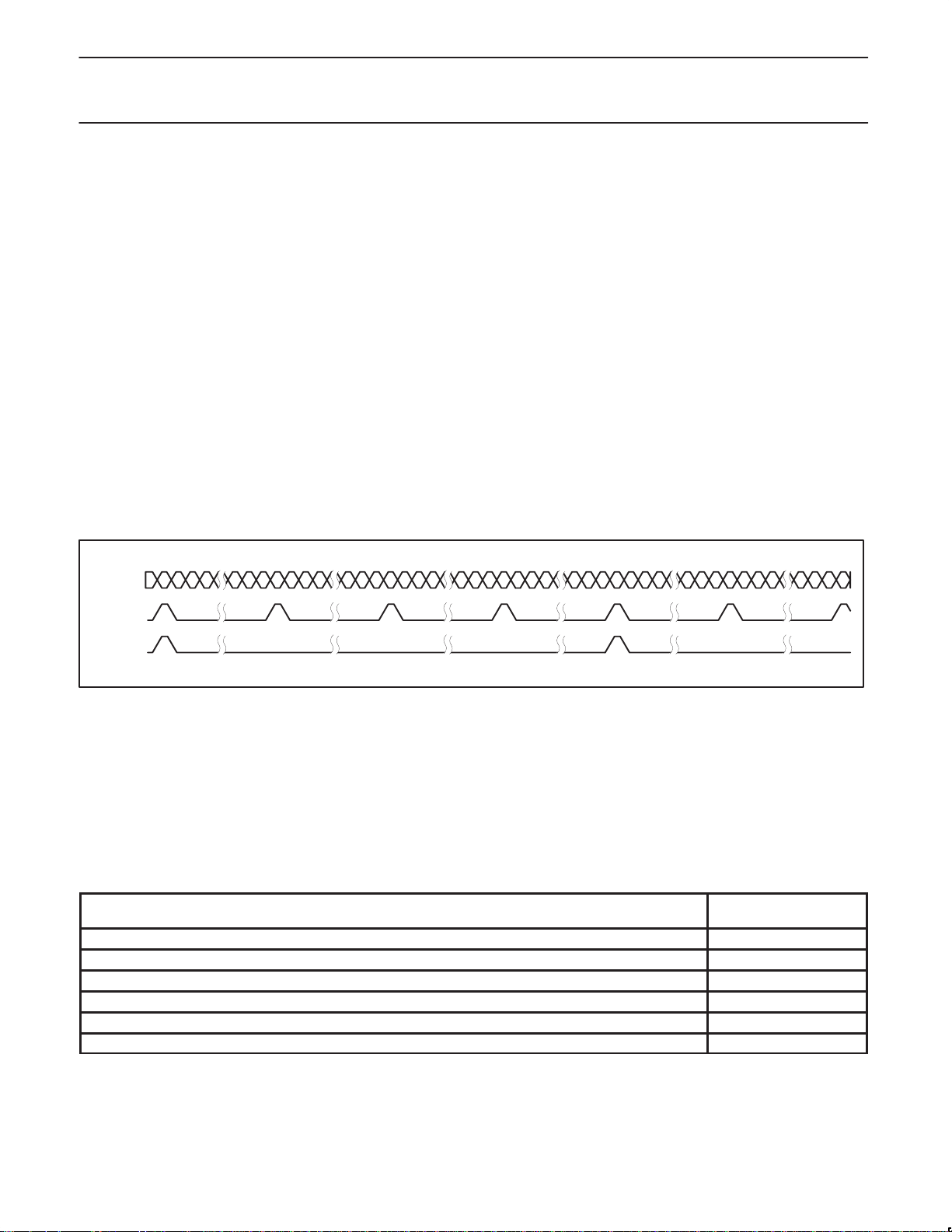
12.2.6 SY – Sync Support
This feature supports the 1394 digital camera specification. The state of this pin will be reflected in the SY bit (ITXCTL register 0x034) and will
be transmitted along with the isochronous data block that was entered with it. The intended use of this pin is to signal the start of a new frame of
video in the isochronous header section of the data payload. Similarly, the isochronous receiver will assert the AVxSY pin simultaneously with
the first byte of the isochronous bus packet in which the SY value was received. NOTE: The SY functionality is only intended to be used when
the M6 cipher and de-cipher are not enabled.
AV DATA
AV SYNC
AV SY
SV01787
Figure 1. Behavior of sysncr
12.2.7 Programmable Buffer Memory
The PDI1394L41 maintains six distinct buffers that are highly configurable to optimize bandwidth capabilities. Buffers can be increased or
decreased from the default value by accessing the indirect address range of 0x100 through 0x1FC (INDADDR, 0x0F8). If the AV Layer is
configured to transmit or receive DVB compliant MPEG-2 type data, the default Isochronous (AV) buf fer sizes are recommended. FIFO sizes
cannot be changed dynamically; after a FIFO size change, transmitters and receivers must be reset.
Buffers can be programmed with 64 quadlet (256 Byte) granularity. Minimum buffer size is 64 quadlets, maximum buffer size is limited to 11 kB.
The sum of all buffers cannot exceed 12K Bytes, or 3K Quadlets.
DEFAULT BUFFER SIZE
BUFFER MEMORY
Asynchronous Receive Response FIFO 256
Asynchronous Receive Request FIFO 256
Asynchronous Transmit Response FIFO 256
Asynchronous Transmit Request FIFO 256
Isochronous (AV) T ransmit Buf fer 1024
Isochronous (AV) Receive Buffer 1024
SIZE
(Quadlets)
2000 Apr 15
11

Philips Semiconductors Preliminary specification
PDI1394L411394 content protection AV link layer controller
12.3 Bushold and Link/PHY single capacitor galvanic isolation
12.3.1 Bushold
The PDI1394L41 uses an internal bushold circuit on each of the indicated pins to keep these CMOS inputs from “floating” while being driven by
a 3-Stated device or input coupling capacitor. Unterminated high impedance inputs react to ambient electrical noise which cause internal
oscillation and excess power supply current draw.
The following pins have bushold circuitry enabled when the ISON pin is in the logic “1” state:
Name Function
PHY CTL0 PHY control line 0
PHY CTL1 PHY control line 1
PHY D0 PHY data bus bit 0
PHY D1 PHY data bus bit 1
PHY D2 PHY data bus bit 2
PHY D3 PHY data bus bit 3
PHY D4 PHY data bus bit 4
PHY D5 PHY data bus bit 5
PHY D6 PHY data bus bit 6
PHY D7 PHY data bus bit 7
Philips bushold circuitry is designed to provide a high resistance pull-up or pull-down on the input pin. This high resistance is easily overcome
by the driving device when its state is switched. Figure 2 shows a typical bushold circuit applied to a CMOS input stage. Two w eak MOS
transistors are connected to the input. An inverter is also connected to the input pin and supplies gate drive to both transistors. When the input
is LOW, the inverter output drives the lower MOS transistor and turns it on. This re-enforces the LOW on the input pin. If the logic device which
normally drives the input pin were to be 3-Stated, the input pin would remain “pulled-down” by the weak MOS transistor. If the driving logic
device drives the input pin HIGH, the inverter will turn the upper MOS transistor on, re-enforcing the HIGH on the input pin. If the driving logic
device is then 3-Stated, the upper MOS transistor will weakly hold the input pin HIGH.
The PHY’s outputs can be 3-Stated and single capacitor isolation can be used with the Link; both situations will allow the Link inputs to float.
With bushold circuitry enabled, these pins are provided with dc paths to ground, and power by means of the bushold transistors; this
arrangement keeps the inputs in known logical states.
INPUT PIN
Figure 2. Bushold circuit
INTERNAL
CIRCUITS
SV00911
2000 Apr 15
12

Philips Semiconductors Preliminary specification
PDI1394L411394 content protection AV link layer controller
12.3.2 Single capacitor isolation
The circuit example (Figure 3) shows the connections required to implement basic single capacitor Link/PHY isolation.
NOTE: The isolation enablement pins on both devices are in their “1” states, activating the bushold circuits on each part. The bushold circuits
provide local dc ground references to each side of the isolating/coupling capacitors. Also note that ground isolation/signal-coupling must be
provided in the form of a parallel combination of resistance and capacitance as indicated in the IEEE 1394 standard.
APPLICATION/LINK
+3.3V
ISON
LINK
PDI1394L41
APPLICATION AND LINK GROUND ISOLATED PHY GROUND
ALSO SEE APPLICATION NOTE AN2452
FOR MORE DETAILS
SCLK
PHY D0
PHY D1
PHY D2
PHY D3
PHY D4
PHY D5
PHY D6
PHY D7
PHYCTL0
PHYCTL1
LREQ
LPS
LINKON
13K
9.1K
LINK
3.3V
C
C
C
C
c
c
c
c
C
L
1MEG Ω
C
c
C
c
C
c
C
c
C
c
C
c
C
c
C
c
C
L
PHY
3.3V
C
c
C
r
ISOLATED/PHY
+3.3V
ISO–
SYSCLK
D0
D1
D2
D3
D4
D5
D6
D7
PHYCTL0
PHYCTL1
LREQ
LPS
LINKON
PHY
PDI1394P2x
VALUES OF THESE RESISTORS DEPEND
ON PHY USED. SEE PHY DATASHEET.
CC = 1 nF; C
= 100 nF; C
r
= 3.3nF
L
SV01816
Figure 3. Single capacitor Link/PHY isolation
12.4 Power Management
The PDI1394L41 implements several features for power management as noted in the
1. Reset of the Phy/Link interface by setting the RPL bit in the LNKCTL register.
2. Disable of the Phy/Link interface caused by either setting the SWPD bit in the RDI register –OR– asserting (high) the PD pin.
3. Initialization of the Phy/Link interface after it was disabled or reset.
The application can power up the Phy/Link interface by deasserting the PD pin –OR– clearing (low) the SWPD in the RDI register. This will
cause the L41 to produce a pulsing signal on the LPS pin. When the L41 is in power down mode, reads and writes to the host interface will be
restricted to those addressing only the RDI register (0x0B0). Please see Section 13.3.11 for further details.
There are 3 ways to power up the L41. (1) When the application wants the 1394 node to resume operation, it simply needs to de–assert the PD
pin, or (2) clear the SWPD bit in the RDI register. The link can also be awakened by another bus node sending a link–on packet to the PHY of
the application’s node. (3) The attached PHY will activate its LinkOn line and the L41 will see the signal and set the LOA bit of the RDI register
(assuming that the ELOA bit is in its enabled, ”1”, state). The L41 will generate an interrupt of the host processor. It will then be up to the host
processor to decide whether to honor the link–on request of the other node. Then the host processor will de–assert the PD pin –OR– clear the
SWPD bit in the RDI register. This activity will power up the L41 causing it to send the pulsing signal out on the LPS pin whic h notifies the
PHYchip of link activity and allows the PHY to discontinue directing the link on signal to the L41. Subsequently, the host processor must
acknowledge the LOA interrupt by writing a ”1” to the LOA bit position in the RDI register after the link on signal from the PHY has stopped.
2000 Apr 15
13
P1394a draft 5.0
. These features include:
Philips Semiconductors Preliminary specification
PDI1394L411394 content protection AV link layer controller
12.5 The host interface
The host interface allows an 8 bit or 16 bit CPU to access all registers and the asynchronous packet queues. It is designed to be easy to use
with a wide range of processors, including 8051, MIPS1900, ST20, PowerPC etc. The host interface can work with 8 bit or 16 bit wide data
paths, and offers multiplexed or non-multiplexed access. There are 64 register addresses (for quadlet wide registers). To access bytes rather
than quadlets the address space is 256 bytes, requiring 8 address lines.
The use of an 8 bit or 16 bit interface introduces an inherent problem that must be solved: register fields can be more than 8 bits wide and be
used (control) or changed (status) at every internal clock tick. If such a field is accessed through an 8 bit or 16 bit interface it requires more than
one read or write cycle, and the value should not change in between to maintain consistency. To overcome this problem accesses to the chip’s
internal register space are always 32 bits, and the host interface must act as a converter between the internal 32 bit accesses and external 8 bit
or 16 bit accesses. This is where the shadow register (0x0F4) is used.
12.5.1 Read accesses
To read an internal register the host interface can make a snapshot (copy) of that specific register which is then made available to the CPU 8 or
16 bits at a time. The register that holds the snapshot copy of the real register value inside the host interface is called the shadow register.
During an 8-bit read cycle address lines HIF A0 and HIF A1 are used to select which of the 4 bytes currently stored in the shadow register is
output onto the CPU data bus. This selection is done by combinatorial logic only, enabling external hardware to toggle these lines through
values 0 to 3 while keeping the chip in a read access mode to get all 4 bytes out very fast (in a single extended read cycle), for example into an
external quadlet register. During a 16 bit read cycle address line HIF A1 is used to select which pair of 4 bytes currently stored in the shadow
register is output to the CPU bus. Again the selection is by combinatorial logic, enabling external hardware to toggle HIF A1 while keeping the
chip in read access mode to get both words very quickly.
This solution requires a control line to direct the host interface to make a snapshot of an internal register when needed, as well as the internal
address of the target register. The register address is connected to input address lines HIF A2..HIF A7, and the update control line to input
address line HIF A8. To let the host interface take a new snapshot the target address must be presented on HIF A2..HIF A7 and HIF A8 must be
raised while executing a read access. The new value will be stored in the shadow register and the selected byte (HIF A0, HIF A1, 8 bit mode)
or word (HIF A1, 16 bit mode) appears on the output.
Not all registers can be accessed in Direct Address Space. Some of the registers are in an indirect address space, these registers control the
FIFO size and content protection system. The correct internal register space has to be selected through the host interface, using directly
addressable registers INDADDR (0x0F8) and INDDATA (0x0FC).
TR
Q
Q
REGISTERS
32
SV01034
CPU
HIF A0..1 (8 BIT MODE)
HIF A1 (16 BIT MODE)
HIF A2..7
HIF A8
MUX MUX
8/16 32 32
SHADOW REGISTER
UPDATE/COPY CONTROL
NOTES:
1. It is not required to read all 4 bytes of a register before reading another register. For example, in 8 bit mode, if only byte 2 of register 0x54 is
required a read of byte address 0x100 + (0×54) + 2 = 0x156 is sufficient.
2. The update control line does not necessarily have to be connected to the CPU address line HIF A8. This input could also be controlled by
other means, for example a combinatorial circuit that activates the update control line whenever a read access is done for byte 0. This
makes the internal updating automatic for quadlet reading.
3. Reading the bytes of the shadow register can be done in any order and as often as needed.
4. It is possible to read/modify/write a register using the shadow register (0x0F4) without rewriting all 4 bytes. For example, to modify an enable
bit in the fourth byte of the Asynchronous Interrupt Enable (0x0A4), a read of location 0x100+0x0A0+3=0x1A3, followed by a write of the
modified byte to the same location 0x100+0x0A0+3=0x1A3 is sufficient. The other bytes remain unchanged.
2000 Apr 15
14

Philips Semiconductors Preliminary specification
PDI1394L411394 content protection AV link layer controller
12.5.2 Write accesses
To write to an internal register the host interface must collect the 4 byte values (8 bit mode) or 2 word values (16 bit mode) into a 32 bit value
and then write the result to the target register in a single clock tick. This requires a register to hold the 32 bit value being compiled until it is
ready to be written to the actual target register. This temporary register inside the host interface is called the shadow register. In 8 bit mode,
address lines HIF A0 and HIF A1 are used to select which of the 4 bytes of the shadow register is to be written with the value on the CPU data
bus. In 16 bit mode, HIF A1 is used to select which half of the shadow register is to be written with the value on the CPU data bus. Only one
byte (8 bit mode) or one word (16 bit mode) can be written in a single write access cycle.
Not all registers can be accessed in Direct Address Space. Some of the registers are in an indirect address space, these registers control the
FIFO size and content protection system. The correct internal register space has to be selected through the host interface, using directly
addressable registers INDADDR (0x0F8) and INDDATA (0x0FC).
TR
Q
Q
REGISTERS
32
SV01035
CPU
HIF A0..1 (8 BIT MODE)
HIF A1 (16 BIT MODE)
HIF A2..7
HIF A8
MUX
MUX
8/16 32
SHADOW REGISTER
UPDATE/COPY CONTROL
NOTES:
1. It is not required to write all 4 bytes, or both words of a register: those bytes that are either reserved (undefined) or don’t care do not have
to be written in which case they will be assigned the value that was left in the corresponding byte of the shadow register from a previous
write access. For example, to acknowledge an interrupt for the isochronous receiver in 8 bit mode, a single byte write to location
0x100+(0x4C)+3 = 0x14F is sufficient. The value 256 represents setting HIF A8=1. The host interface cannot directly access the FIFOs, but
instead reads from/writes into a transfer register (shown as TR in the Figures above). Data is moved between FIFO and TR by internal logic
as soon as possible without CPU intervention.
2. The update control line does not necessarily have to be connected to the CPU address line HIF A8. This input could also be controlled by
other means, for example a combinatorial circuit that activates the update control line whenever a write access is done for byte 3 or the
upper 16 bits. This makes the internal updating automatic for quadlet writing.
3. Writing the bytes or words of the shadow register can be done in any order and as often as needed (new writes simply overwrite the old
value).
4. It is now possible to read/modify/write a register using the shadow register (0x0F4) without rewriting all 4 bytes. For example, to modify an
enable bit in the fourth byte of the Asynchronous Interrupt Enable (0x0A4), a read of location 0x100+0x0A0+3=0x1A3, followed by a write of
the modified byte to the same location 0x100+0x0A0+3=0x1A3 is sufficient. The other bytes remain unchanged.
2000 Apr 15
15

Philips Semiconductors Preliminary specification
PDI1394L411394 content protection AV link layer controller
12.5.3 Big and little endianness, data invariance, and data bus width
The host interface offers programmable endianness, data invariance, and selectable 8 and 16 bit data widths. L TLEND (pin 121) and DATINV
(pin 122) are multiplexed configuration pins that will be sampled on the trailing edge of RESET; the states of these pins are established by
connecting each pin to the proper logic state, ground or V
register (0x0F4) will be preset to a value of 0x0F0A0500 after a power reset. Table 1 describes the configurations.
Table 1. Configuration possible combinations
LTLEND (Little Endian) DATINV (Data Invariant) HIF 16BIT Result
1 1 See Table 2 Byte/Word address is reversed
1 0 1 Bytes are swapped within the word
0 X 1 16-bit data bus, address as in PDI1394L21
0 X 0 8-bit data bus, address as in PDI1394L21
Table 2. Explanation of the mode LittleEnd = 1, DataInvariant = 1
HIF16 = 0 HIF16 = 1
Outside Address (A1, A0) Inside Address (A1, A0) Outside Address (A1, A0) Inside Address (A1, A0)
00 11 0X 1X
01 10 0X 1X
10 01 1X 0X
11 00 1X 0X
, through a resistor, 22 kΩ is recommended. To verify the configuration, the shadow
DD
It is important to note that some operands in the indirect address space consist of more than one quadlet. For these operands, the lowest
address always contains the most significant quadlet.
In Bit Endian mode and DATAINV = 0, the bytes in each quadlet are numbered 0..3 from left (most significant) to right (least significant) as
shwon in Figure 4.
To access a register in 8 bit HIF mode, at address N the CPU should use addresses E:
E = N ; to access the upper 8 bits of the register.
E = N + 1 ; to access the upper middle 8 bits of the register.
E = N + 2 ; to access the lower middle 8 bits of the register.
E = N + 3 ; to access the lower 8 bits of the register.
To access a register in 16 bit HIF mode, at internal address N, the CPU should use addresses E:
E = N ;to access the upper 16 bits of the register
E = N + 2 ;to access the lower 16 bits of the register
29 28 27 2625 24 23 22 21 20 19 18 17 16 15 14 13 12 11 10 9 8 7 6 5 4 3 2 1 0
3130
BYTE 0 BYTE 1
BYTE 2
BYTE 3
SV00656
Figure 4. Byte order in quadlets as implemented in the host interface, HIF LTLEND = LOW
2000 Apr 15
16

Philips Semiconductors Preliminary specification
PDI1394L411394 content protection AV link layer controller
In Little Endian mode and DATAINV = 0, the bytes in each quadlet are numbered 3. .0 from the left (most significant) to right (least significant)
as shown in Figure 5. To access a register in 8 bit HIF mode, at address N the CPU should use addresses E:
E = N + 3 ;to access the upper 8 bits of the register
E = N + 2 ;to access the upper middle 8 bits of the register
E = N + 1 ;to access the lower middle 8 bits of the register
E = N ;to access the lower 8 bits of the register
To access a register in 16 bit HIF mode, at internal address N, the CPU should used addresses E:
E = N ;to access the lower 16 bits of the register
E = N + 2 ;to access the upper 16 bits of the register
29 28 27 2625 24 23 22 21 20 19 18 17 16 15 14 13 12 11 10 9 8 7 6 5 4 3 2 1 0
3130
BYTE 3 BYTE 2
BYTE 1
BYTE 0
SV01079
Figure 5. Byte order in quadlets as implemented in the host interface, HIF LTLEND = HIGH
12.5.4 Accessing the asynchronous packet queues
Although entire incoming packets are stored in the receiver buffer memory they are not randomly accessible. These buffers act like FIFOs and
only the frontmost (oldest) data quadlet entry is accessible for reading. Therefore only one location (register address) is allocated to each of the
two receiver queues. Reading this location returns the head entry of the queue, and at the same time removes it from the queue, making the
next stored data quadlet accessible.
With the current host interface such a read is in fact a move operation of the data quadlet from the queue to the shadow register. Once the data
is copied into the shadow register it is no longer available in the queue itself so the CPU should always read all 4 bytes, or both words, before
attempting any other read access (be careful with interrupt handlers for the PDI1394L41!).
2000 Apr 15
17
Philips Semiconductors Preliminary specification
PDI1394L411394 content protection AV link layer controller
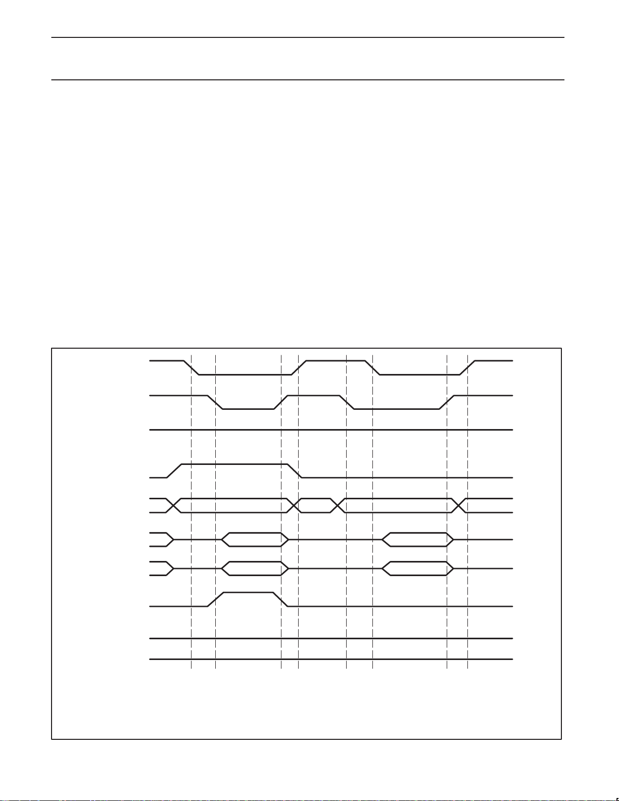
12.5.5 The CPU bus interface signals
The CPU interface is directly compatible with a wide range of microcontrollers, and supports both multiplexed and non-multiplex access. It uses
separate HIF RDN, HIF WRN, HIF ALE, and HIF CSN chip select lines. There are 9 address inputs (HIF A0..HIF A8) and 8 or 16 data in/out
lines HIF D[7:0] or HIF D [15:0]. The upper 8 bits of the data in/out lines are only used when the 8/16 bit mode pin (HIF16BIT) is held HIGH.
The CPU is not required to run a clock that is synchronous to the 1394 base clock. The control signals will be resampled by the host interface
before being used internally.
In non-multiplex mode (HIF MUX = LOW), an access through the host interface starts when HIF CSN = 0 and either HIF WRN = 0 or HIF RDN = 0.
Typically the chip select signal is derived from the upper address lines of the CPU (address decode stage), but it could also be connected to a
port pin of the CPU to avoid the need for an external address decoder in very simple CPU systems. When both HIF CSN = 0 and HIF RDN = 0
the host interface will start a read access cycle, so the cycle is triggered at the falling edge of either HIF CSN or HIF RDN, whichever is later.
In multiplex mode (HIF MUX = HIGH), an access through the host interface starts when HIF CSN = 0 and either HIF WRN = 0 or HIF RD_N = 0.
The address must now be presented on the HIF AD [7:0] lines, and will be latched on the falling edge of ALE. If HIF RDN = 0, data will be
offered after the falling edge of ALE. If HIF WRN = 0, data has to be presented by the microcontroller.
In both multiplexed and non-multiplexed mode, HIF W AIT can be used to signal to the controlling CPU that an extension of the current access
cycle is needed. This allows the PDI1394L41 to work in the same address space as peripherals with a shorter access time. HIF WAIT will
remain HIGH for the minimum duration of the access cycle. If HIF A[8] is HIGH, HIF WAIT will extend the access cycle to 120ns to allow for the
shadow register transfer to take place. Subsequent access to the same register which does not required A[8] to be raised, can be executed
much faster. By connecting HIF WAIT to the appropriate input on the controlling processor, the PDI1394L41 can be mapped in memory space
with faster devices. The PDI1394L41 should not be mapped in memory space with devices that require access faster than 15 ns.
HIF A[7:0] can be used as a simple demultiplexer. In multiplex mode, the address on AD[7:0] will appear on A[7:0] immediately, and will remain
there until the next rising edge of HIF ALE.
HIF CS_N
HIF RD_N
HIF WR_N
HIF A8
HIFA7–A0
HIFD15–D8
HIFAD7–AD0
HIF_WAIT
HIF_MUX
HIF16BIT
NOTE: ALE line is held LOW.
2000 Apr 15
An extended read cycle may be implemented by holding CS_N and RD_N low (active)
and changing only the A7–A0 address. After each new address stabilizes, wait at least
and read the data. The extended read cycle can be used only following a read of
t
ACC
the first byte of the shadow register using the A8 transfer mechanism. See the section
on Read Accesses (12.5.1).
Figure 6. 16 Bit Read Cycle Non-multiplexed
18
SV01088

Philips Semiconductors Preliminary specification
PDI1394L411394 content protection AV link layer controller
HIF CS_N
HIF RD_N
HIF WR_N
HIFA7–A0
HIFD15–D8
HIFAD7–AD0
A8
HIF_WAIT
HIF_MUX
HIF16BIT
NOTE: ALE line is held LOW.
SV01089
Figure 7. 16 Bit Write Cycle Non-multiplexed
2000 Apr 15
19

Philips Semiconductors Preliminary specification
PDI1394L411394 content protection AV link layer controller
HIF CS_N
HIF ALE
AD7–AD0
A7–A0
HIFD15–D8
A8
HIF RD_N
HIF WR_N
HIF_WAIT
HIF_MUX
HIF16BIT
Note: Second write cycle elongated by WAIT signal.
Figure 8. 16 Bit Write Cycle Multiplexed
ADDR DATADATA ADDR
LATCHED LATCHED
DATADATA
SV01090
2000 Apr 15
20

Philips Semiconductors Preliminary specification
PDI1394L411394 content protection AV link layer controller
HIF CS_N
HIF ALE
HIF AD7–AD0
HIF A7–A0
HIFD15–D8
HIF RD_N
HIF WR_N
HIF_WAIT
HIF_MUX
HIF16BIT
ADDR ADDRDA TA DA TA
LATCHED LATCHED
DATADATA
A8
SV01091
Figure 9. 16 Bit Read Cycle Multiplexed
2000 Apr 15
21
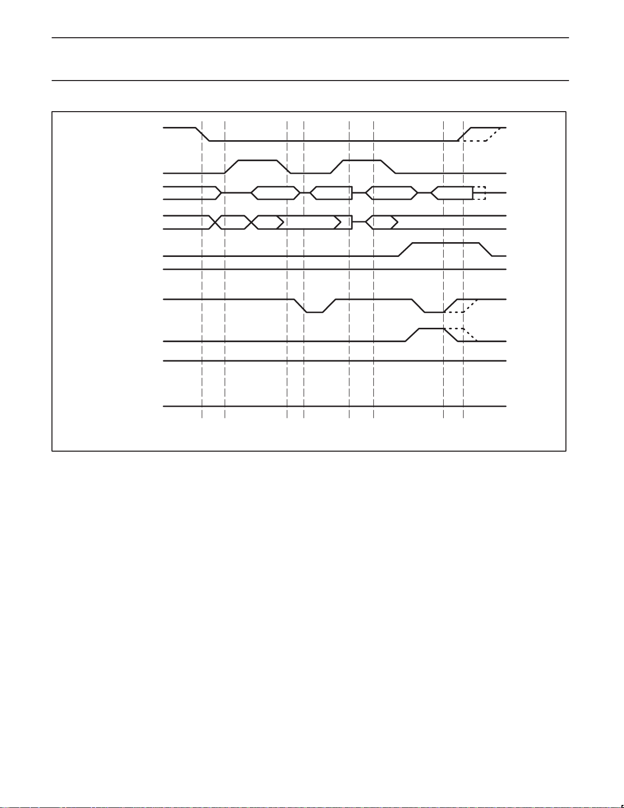
Philips Semiconductors Preliminary specification
PDI1394L411394 content protection AV link layer controller
HIF CS_N
HIF ALE
AD7–AD0
A7–A0
HIF RD_N
HIF WR_N
HIF_WAIT
HIF_MUX
HIF16BIT
ADDR DATADATA ADDR
LATCHED LATCHED
A8
SV01772
Figure 10. 8 Bit Write Cycle Multiplexed
2000 Apr 15
22
 Loading...