

Philips PDI1394L21 Datasheet

INTEGRATED CIRCUITS
NOTICE:
SEE ATTACHED ERRATA WHICH FOLLOWS THIS DOCUMENT FOR INFORMATION
REGARDING CHANGED SPECIFICATIONS
PDI1394L21
1394 full duplex AV link layer controller
Preliminary specification
Supersedes data of 1999 Mar 30
1999 Aug 06
Philips Semiconductors Preliminary specification
PDI1394L211394 full duplex AV link layer controller
1.0 FEATURES
•IEEE 1394–1995 Standard Link Layer Controller
•Hardware Support for the IEC61883 International Standard of
Digital Interface for Consumer Electronics
•Interface to any IEEE 1394–1995 Physical Layer Interface
•5V Tolerant I/Os
•Single 3.3V supply voltage
•Full-duplex isochronous operation
•Operates with 400/200/100 Mbps physical layer devices
•Dual 4K Byte FIFOs for isochronous data
•Supports single capacitor isolation mode and IEEE 1394–1995,
Annex J. isolation
•4-field deep SYT buffer added to enhance real-time isochronous
synchronization using the AVFSYNC pin
•Generates its own AV port clocks under software control. Select
one of three frequencies: 24.576, 12.288, or 6.144 MHz
2.0 DESCRIPTION
The PDI1394L21, Philips Semiconductors Full Duplex 1394
Audio/Video (AV) Link Layer Controller, is an IEEE 1394–1995
compliant link layer controller featuring 2 embedded AV layer
interfaces. The AV layers are designed to pack and un-pack
application data packets for transmission over the IEEE 1394 bus
using isochronous data transfers. Because of its full duplex
architecture, the PDI1394L21 is capable of receiving and
transmitting isochronous data during the same bus cycle. Two 8 bit
AV ports, each with its own buffer (FIFO), receive and output
isochronous data for transmission and reception of bus packets.
Each port can be configured to receive or transmit, however, the
other port always performs the opposite function. Half duplex
operation is also permitted.
The application data is packetized according to the IEC 61883
International Standard of Interface for Consumer Electronic
Audio/Video Equipment. Both AV layer interfaces are byte-wide
ports capable of accommodating various MPEG–2 and DVC
codecs. An 80C51 compatible byte-wide host interface is provided
for internal register configuration as well as performing
asynchronous data transfers.
The PDI1394L21 is powered by a single 3.3V power supply and the
inputs and outputs are 5V tolerant. It is available in the LQFP100
and TQFP100 packages.
3.0 QUICK REFERENCE DATA
GND = 0V; T
SYMBOL
V
DD
I
DD
SCLK Device clock 49.147 49.152 49.157 MHz
= 25°C
amb
PARAMETER CONDITIONS MIN TYP MAX UNIT
Functional supply voltage range 3.0 3.3 3.6 V
Supply current @ VDD = 3.3V Operating 75 mA
4.0 ORDERING INFORMATION
PACKAGES TEMPERATURE RANGE OUTSIDE NORTH AMERICA NORTH AMERICA PKG. DWG. #
100-pin plastic LQFP100 0°C to +70°C PDI1394L21BE PDI1394L21BE SOT407 AB15
100-pin plastic TQFP100 0°C to +70°C PDI1394L21BP PDI1394L21BP SOT386 BB2
NOTE:
This datasheet is subject to change.
Please visit out internet website www.semiconductors.philips.com/1394 for latest changes.
1999 Aug 06
2

Philips Semiconductors Preliminary specification
PDI1394L211394 full duplex AV link layer controller
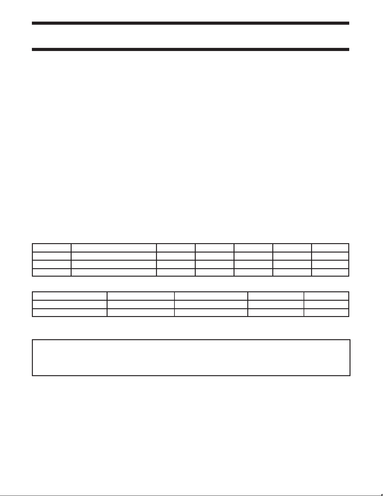
5.0 PIN CONFIGURATION
100 76
Pin Function
1 HIF D7
2 HIF D6
3 HIF D5
4 HIF D4
5 GND
6V
DD
7 HIF D3
8 HIF D2
9 HIF D1
10 HIF D0
11 CLK25
12 GND
13 V
DD
14 HIF A8
15 HIF A7
16 HIF A6
17 HIF A5
18 HIF A4
19 HIF A3
20 HIF A2
21 HIF A1
22 HIF A0
23 GND
24 V
DD
25 HIF CS_N
26 HIF WR_N
27 HIF RD_N
28 HIF INT_N
29 RESET_N
30 CYCLE IN
31 GND
32 V
DD
33 CYCLE OUT
34 PHY D7*
1
25
26 50
TQFP
LQFP
Pin Function
35 PHY D6*
36 PHY D5*
37 PHY D4*
38 GND
39 V
DD
40 PHY D3*
41 PHY D2*
42 PHY D1*
43 PHY D0*
44 GND
45 V
DD
46 PHY CTL1*
47 PHY CTL0*
48 ISO_N
49 V
DD
50 GND
51 N/C
52 AV1ERR1
53 AV1ERR0
54 LREQ*
55 SCLK
56 AV1ENDPCK
57 AV1SYNC
58 AV1CLK
59 AV1FSYNC
60 AV1ENKEY
61 AV1VALID
62 N/C
63 GND
64 V
DD
65 RESESRVED
66 RESERVED
67 RESERVED
68 AV1 D0
75
51
Pin Function
69 AV1 D1
70 AV1 D2
71 AV1 D3
72 V
DD
73 GND
74 AV1 D4
75 AV1 D5
76 AV1 D6
77 AV1 D7
78 V
DD
79 GND
80 AV2ERR1
81 AV2ERR0
82 AV2ENDPCK
83 AV2SYNC
84 AV2CLK
85 AV2FSYNC
86 AV2VALID
87 GND
88 V
DD
89 AV2 D0
90 AV2 D1
91 AV2 D2
92 AV2 D3
93 GND
94 V
DD
95 AV2D4
96 AV2 D5
97 AV2 D6
98 AV2 D7
99 AV2ENKEY
100 N/C
* INDICATES PIN EQUIPPED WITH INTERNAL BUS HOLD CIRCUIT
ACTIVATED BY THE STATE OF THE ISO_N PIN.
1999 Aug 06
SV00877
3
Philips Semiconductors Preliminary specification
PDI1394L211394 full duplex AV link layer controller
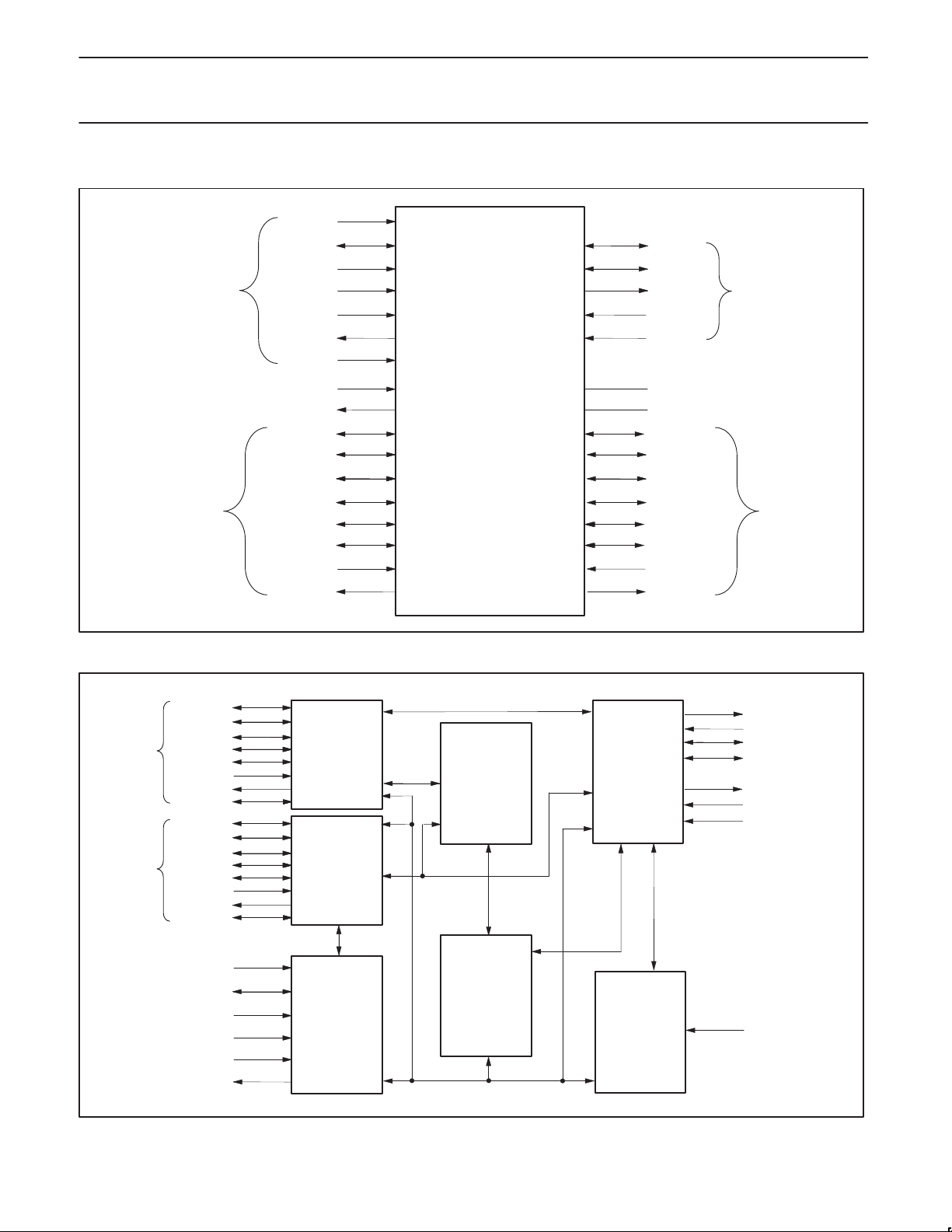
6.0 FUNCTIONAL DIAGRAM
HIF A[8:0]
HOST
HIF D[7:0]
HIF WR_N
HIF RD_N
HIF CS_N
HIF INT_N
RESET_N
PHY D[0:7]
PHY CTL[0:1]
LREQ
ISO_N
SCLK
PHY
CYCLEIN
CYCLEOUT
AV1 D[7:0]
AV1CLK
AV1VALID
AV1SYNC
AV1FSYNC AV2FSYNC
AV LAYER 1
AV1ENKEY
AV1ENDPCK
AV1ERR[1:0]
7.0 INTERNAL BLOCK DIAGRAM
AV1 D[7:0]
AV1CLK
AV1ENDPCK
AV LAYER1
AV1ERR[0:1]
AV2ENDPCK
AV2ERR[0:1]
AV LAYER2
AV1SYNC
AV1VALID
AV1FSYNC
AV1ENKEY
AV2 D[7:0]
AV2CLK
AV2SYNC
AV2VALID
AV2FSYNC
AV2ENKEY
HIF A[8:0]
HIF D[7:0]
HIF WR_N
HIF RD_N
HIF CS_N
HIF INT_N
AV1 LAYER
ISOCHRONOUS
TRANSMITTER/
RECEIVER
AV2 LAYER
ISOCHRONOUS
TRANSMITTER/
RECEIVER
INTERFACE
8-BIT
PDI1394L21
IEEE 1394
FULL DUPLEX
AV LINK LAYER CONTROLLER
9KB BUFFER
MEMORY
(ISOCH & ASYNC
PACKETS)
ASYNC
TRANSMITTER
AND
RECEIVER
VDD
GND
AV2D[7:0]
AV2CLK
AV2VALID
AV2SYNC
AV2ENKEY
AV2ENDPCK
AV2ERR[1:0]
LINK CORE
CONTROL
AND
STATUS
REGISTERS
AV LAYER 2
SV00878
CYCLEOUT
CYCLEIN
PHY D[0:7]
PHY CTL[0:1]
LREQ
ISO_N
SCLK
NOTE: THERE IS ONLY ONE
ISOCHRONOUS RECEIVER
AND ONE ISOCHRONOUS
TRANSMITTER—THEREFORE,
WHEN EITHER AVPORT IS SET
TO TRANSMIT, THE OTHER
AVPORT IS AUTOMATICALLY
SET TO RECEIVE.
RESET_N
1999 Aug 06
SV00879
4

Philips Semiconductors Preliminary specification
PDI1394L211394 full duplex AV link layer controller
8.0 APPLICATION DIAGRAM
MPEG OR DVC
DECODER
MPEG OR DVC
DECODER
HOST CONTROLLER
AV
INTERFACE
AV
INTERFACE
DATA 8/
ADDRESS 9/
INTERRUPT & CONTROL
PDI1394L21
AV LINK
PHY–LINK
INTERFACE
9.0 PIN DESCRIPTION
9.1 Host Interface
PIN No. PIN SYMBOL I/O NAME AND FUNCTION
1, 2, 3, 4, 7, 8,
9, 10
5, 12, 23, 31,
38, 44, 50, 63,
73, 79, 87, 93
6, 13, 24, 32,
39, 45, 49, 64,
72, 78, 88, 94
14, 15, 16, 17,
18, 19, 20, 21,
22
25 HIF CS_N I
26 HIF WR_N I
27 HIF RD_N I
28 HIF INT_N O
29 RESET_N I Reset (active LOW). The asynchronous master reset to the PDI1394L21.
HIF D[7:0] I/O Host Interface Data 7 (MSB) through 0. Byte wide data path to internal registers.
GND Ground reference
V
DD
HIF A[8:0] I
3.3V ± 0.3V power supply
Host Interface Address 0 through 8. Provides the host with a byte wide interface to internal
registers. See description of Host Interface for addressing rules.
Chip Select (active LOW). Host bus control signal to enable access to the FIFO and control and
status registers.
Write enable. When asserted (LOW) in conjunction with HIF CS_N, a write to the PDI1394L21
internal registers is requested. (NOTE: HIF WR_N and HIF RD_N : if these are both LOW in
conjunction with HIF CS_N, then a write cycle takes place. This can be used to connect CPUs
that use R/W_N line rather than separate RD_N and WR_N lines. In that case, connect the
R/W_N line to the HIF WR_N and tie HIF RD_N LOW.)
Read enable. When asserted (LOW) in conjunction with HIF CS_N, a read of the PDI1394L21
internal registers is requested.
Interrupt (active LOW). Indicates a interrupt internal to the PDI1394L21. Read the General
Interrupt Register for more information. This pin is open drain and requires a 1KW pull-up resistor.
PDI1394Pxx
PHY
1394 CABLE
INTERFACE
SV00880
1999 Aug 06
5
Philips Semiconductors Preliminary specification
PDI1394L211394 full duplex AV link layer controller
9.2 AV Interface 1
NOTE: This AV interface may be configured to transmit or receive according to the condition of “DIRAV1” bit in GLOBCSR register
(0X018)—default is transmit.
PIN No.
77, 76, 75, 74,
71, 70, 69, 68
58 AV1CLK I/O
57 AV1SYNC I/O Start of packet indicator; should only be used when AV1VALID is active.
59 AV1FSYNC I/O
56 AV1ENDPCK I
60 AV1ENKEY I/O
61 A V1VALID I/O Indicates data on AV1 D [7:0] is valid.
53 AV1ERR0 O
52 AV1ERR1 O Sequence Error. Indicates at least one source packet was lost before the current AV1 D [7:0] data.
PIN SYMBOL I/O NAME AND FUNCTION
AV1 D[7:0] I/O Audio/Video Data 7 (MSB) through 0. Byte-wide interface to the AV layer 1.
External application clock. Rising edge active. This pin can be programmed to output the
application clock. Depending on the configuration of AV Port 1 as transmitter or receiver , the
output enable is located in the ITXPKCTL register (address 0x020) or IRXPKCTL register
(address 0x040).
Programmable frame sync, can be set to input. Frame sync input used for Digital Video (DV). The
signal is time stamped and transmitted in the SYT field of ITXHQ2. Frame sync output. Signal is
derived from SYT field of IRXHQ2.
End of application packet indication from data source. Required only if input packet is not multiple
of 4 bytes. It can be tied LOW for data packets that are 4*N in size.
Encryption key state. Indicates state “1” or “0” of encryption key which matches present port data
during receive mode. Used to input key state during transmit mode.
CRC error, indicates bus packet containing AV1 D [7:0] had a CRC error, the current AV packet is
unreliable.
9.3 AV Interface 2
NOTE: This AV interface may be configured to transmit or receive according to the condition of “DIRAV1” bit in GLOBCSR register—default is
receive.
PIN No.
98, 97, 96, 95,
92, 91, 90, 89
84 AV2CLK I/O
83 AV2SYNC I/O Start of packet indicator; should only be used when AV2VALID is active.
85 AV2FSYNC I/O
82 AV2ENDPCK I
86 A V2VALID I/O Indicates data on AV2 D [7:0] is valid.
81 AV2ERR0 O
80 AV2ERR1 O Sequence Error. Indicates at least one source packet was lost before the current AV2 D [7:0] data.
99 AV2ENKEY I/O
PIN SYMBOL I/O NAME AND FUNCTION
AV2 D[7:0] I/O Audio/Video Data 7 (MSB) through 0. Byte-wide interface to the AV layer 2.
External application clock. Rising edge active. This pin can be programmed to output the
application clock. Depending on the configuration of AV Port 2 as transmitter or receiver , the
output enable is located in the ITXPKCTL register (address 0x020) or IRXPKCTL register
(address 0x040).
Programmable frame sync, can be set to input or output. Frame sync input used for Digital Video
(DV). The signal is time stamped and transmitted in the SYT field of ITXHQ2. Frame sync output.
Signal is derived from SYT field of IRXHQ2.
End of application packet indication from data source. Required only if input packet is not multiple
of 4 bytes. It can be tied LOW for data packets that are 4*N in size.
CRC error, indicates bus packet containing AV2 D [7:0] had a CRC error, the current AV packet is
unreliable.
Encryption key state. Indicates state “1” or “0” of encryption key which matches present port data
during receive mode. Used to input key state during transmit mode.
9.4 Phy Interface
PIN No. PIN SYMBOL I/O NAME AND FUNCTION
Data 0 (MSB) through 7 (NOTE: To preserve compatibility to the specified Link-Phy interface of
43, 42, 41, 40,
37, 36, 35, 34
47, 46 PHY CTL[0:1] I/O Control Lines between Link and Phy . See 1394 Specification for more information.
48 ISO_N I
54 LREQ O
55 SCLK I System clock. 49.152MHz input from the PHY (the PHY -LINK interface operates at this frequency).
PHY D[0:7] I/O
the IEEE 1394–1995 standard, Annex J, bit 0 is the most significant bit). Data is expected on
PHY D[0:1] for 100Mb/s, PHY D[0:3] for 200Mb/s, and PHY D[0:7] for 400Mb/s. See IEEE
1394–1995 standard, Annex J for more information.
Isolation mode. This pin is asserted (LOW) when an Annex J type isolation barrier is used.
See IEEE 1394–1995 Annex J. for more information. When tied HIGH, this pin enables internal
bushold circuitry on the affected PHY interface pins (see below). Active bushold circuits allow
either the direct connection to PHY pins or the use of the single capacitor isolation mode.
Link Request. Bus request to access the PHY. See IEEE 1394–1995 standard, Annex J for more
information. (Used to request arbitration or read/write PHY registers).
1999 Aug 06
6
Philips Semiconductors Preliminary specification
PDI1394L211394 full duplex AV link layer controller
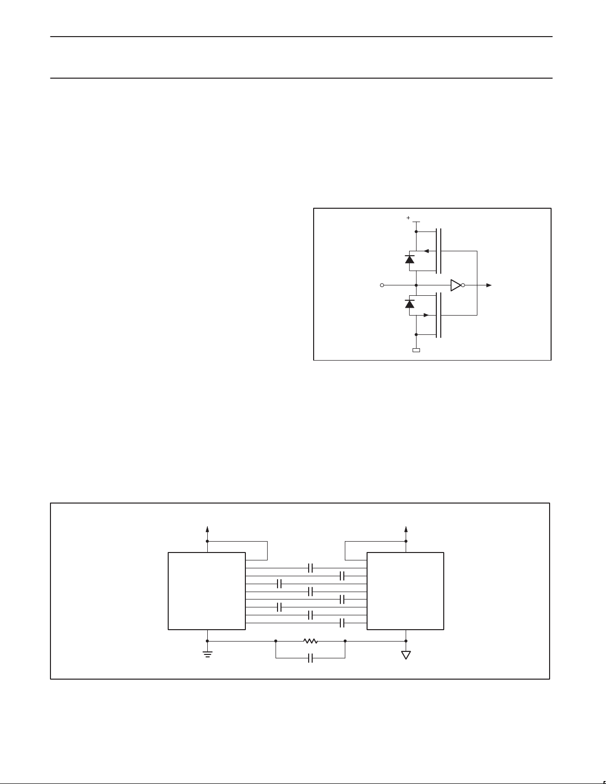
9.4.1 Bushold and Link/PHY single capacitor
galvanic isolation
9.4.1.1 Bushold
The PDI1394L21 uses an internal bushold circuit on each of the
indicated pins to keep these CMOS inputs from “floating” while being
driven by a 3-Stated device or input coupling capacitor.
Unterminated high impedance inputs react to ambient electrical
noise which cause internal oscillation and excess power supply
current draw.
The following pins have bushold circuitry enabled when the ISO_N
pin is in the logic “1” state:
Pin No. Name Function
47 PHYCTL0 PHY control line 0
46 PHYCTL1 PHY control line 1
54 LREQ Link request line
43 PHYD0 PHY data bus bit 0
42 PHYD1 PHY data bus bit 1
41 PHYD2 PHY data bus bit 2
40 PHYD3 PHY data bus bit 3
37 PHYD4 PHY data bus bit 4
36 PHYD5 PHY data bus bit 5
35 PHYD6 PHY data bus bit 6
34 PHYD7 PHY data bus bit 7
Philips bushold circuitry is designed to provide a high resistance
pull-up or pull-down on the input pin. This high resistance is easily
overcome by the driving device when its state is switched. Figure 1
shows a typical bushold circuit applied to a CMOS input stage. Two
weak MOS transistors are connected to the input. An inverter is also
connected to the input pin and supplies gate drive to both
transistors. When the input is LOW, the inverter output drives the
lower MOS transistor and turns it on. This re-enforces the LOW on
the input pin. If the logic device which normally drives the input pin
were to be 3-Stated, the input pin would remain “pulled-down” by the
weak MOS transistor. If the driving logic device drives the input pin
HIGH, the inverter will turn the upper MOS transistor on,
re-enforcing the HIGH on the input pin. If the driving logic device is
then 3-Stated, the upper MOS transistor will weakly hold the input
pin HIGH.
The PHY’s outputs can be 3-Stated and single capacitor isolation
can be used with the Link; both situations will allow the Link inputs to
float. With bushold circuitry enabled, these pins are provided with dc
paths to ground, and power by means of the bushold transistors;
this arrangement keeps the inputs in known logical states.
INPUT PIN
INTERNAL
CIRCUITS
SV00911
Figure 1. Bushold circuit
9.4.1.2 Single capacitor isolation
The circuit example (Figure 2) shows the connections required to
implement basic single capacitor Link/PHY isolation.
NOTE: The isolation enablement pins on both devices are in their
“1” states, activating the bushold circuits on each part. The bushold
circuits provide local dc ground references to each side of the
isolating/coupling capacitors. Also note that ground
isolation/signal-coupling must be provided in the form of a parallel
combination of resistance and capacitance as indicated in
IEEE 1394–1995.
1999 Aug 06
APPLICATION
6, 13, 24, 32, etc.
LINK
PDI1394L21
APPLICATION GROUND
+3.3V
48
ISO_N
PHY D0
PHY D1
PHY D2
PHY D3
PHYCTL0
PHYCTL1
LREQ
SCLK
43
42
41
40
47
46
54
55
Cc
Cc
Cc = 0.001µF; Cr = 0.1µF
Cc
Cc
Cc
1MEG Ω
Cr
Figure 2. Single capacitor Link/PHY isolation
7
ISOLATED
+3.3V
ISO–
D0
Cc
Cc
Cc
D1
PDI1394Pxx
D2
D3
PHYCTL0
PHYCTL1
LREQ
SYSCLK
PHY
ISOLATED PHY GROUND
SV00912
Philips Semiconductors Preliminary specification
SYMBOL
PARAMETER
CONDITIONS
UNIT
SYMBOL
PARAMETER
CONDITIONS
UNIT
PDI1394L211394 full duplex AV link layer controller
9.5 Other Pins
PIN No. PIN SYMBOL I/O NAME AND FUNCTION
65, 66, 67 RESERVED NA
51, 62, 100 N/C NA These pins should not be connected or terminated.
30 CYCLEIN I
33 CYCLEOUT O Reproduces the 8kHz cycle clock of the cycle master.
11 CLK25 O Auxiliary clock, value is SCLK/2 (usually 24.576 MHz)
10.0 RECOMMENDED OPERATING CONDITIONS
V
CC
V
V
V
I
OH
I
OL
dT/dV Input transition rise or fall time 0 20 ns/V
T
amb
SCLK System clock 49.147 49.157 MHz
AVCLK AV interface clock 0 24 MHz
t
t
DC supply voltage 3.0 3.6 V
Input voltage 0 5 V
I
High-level input voltage 2.0 V
IH
Low-level input voltage 0.8 V
IL
High-level output current 8 mA
Low-level output current –8 mA
Operating ambient temperature range 0 +70 °C
Input rise time 10 ns
r
input fall time 10 ns
f
These pins are reserved for factory testing. For normal operation they should be connected to
ground.
Provides the capability to supply an external cycle timer signal for the beginning of 1394 bus
cycles.
LIMITS
MIN. MAX.
11.0 ABSOLUTE MAXIMUM RATINGS
1, 2
In accordance with the Absolute Maximum Rating System (IEC 134). Voltages are referenced to GND (ground = 0V).
LIMITS
MIN MAX
I
GND
T
V
T
P
DD
I
IK
V
I
OK
V
I
stg
amb
DC supply voltage –0.5 +4.6 V
DC input diode current – –50 mA
DC input voltage –0.5 +5.5 V
I
DC output diode current – ±50 mA
DC output voltage –0.5 VDD +0.5 V
O
DC output source or sink current – ±50 mA
O
, I
DC VCC or GND current – ±150 mA
CC
Storage temperature range –60 150 °C
Operating ambient temperature 0 70 °C
Power dissipation per package 0.6 W
tot
NOTES:
1. Stresses beyond those listed may cause permanent damage to the device. These are stress ratings only and functional operation of the
device at these or any other conditions beyond those indicated under “recommended operating conditions” is not implied. Exposure to
absolute-maximum-rated conditions for extended periods may affect device reliability .
2. The performance capability of a high-performance integrated circuit in conjunction with its thermal environment can create junction
temperatures which are detrimental to reliability. The maximum junction temperature of this integrated circuit should not exceed 150°C.
1999 Aug 06
8
Philips Semiconductors Preliminary specification
PDI1394L211394 full duplex AV link layer controller
11.1 Buffer Memory Sizes
BUFFER MEMORY
Asynchronous Receive Response FIFO 64
Asynchronous Receive Request FIFO 128
Asynchronous Transmit Response FIFO 64
Asynchronous Transmit Request FIFO 64
Isochronous (AV) T ransmit Buf fer 1024
Isochronous (AV) Receive Buffer 1024
12.0 FUNCTIONAL DESCRIPTION
12.1 Overview
The PDI1394L21 is an IEEE 1394–1995 compliant link layer controller. It provides a direct interface between a 1394 bus and various MPEG–2
and DVC codecs. Via this interface, the AV Link maps and unmaps these AV datastreams from these codecs onto 1394 isochronous bus
packets. The AV Link also provides an 8051 compatible microcontroller interface for an attached host controller. Through the host interface port,
the host controller can configure the AV layer for transmission or reception of AV datastreams. The host interface port also allows the host
controller to transmit and receive 1394 asynchronous data packets.
12.2 AV interface and AV layer
The AV interface and AV layer allow AV packets to be transmitted from one node to another. The AV transmitter and receiver within the AV layer
perform all the functions required to pack and unpack AV packet data for transfer over a 1394 network. Once the AV layer is properly configured
for operation, no further host controller service should be required. The operation of the AV layer is full-duplex, i.e., the AV layer can receive and
transmit AV packets at the same time.
12.2.1 The AV Interface
The AV Link provides an 8 bit data path to the AV layer. The 8 bit data path is designed with associated clock and control signals to be
compatible with various MPEG–2 and DVC codecs.
The AV interface port buf fer, if so programmed, can time stamp incoming AV packets. The AV packet data is stored in the embedded memory
buffer , along with its time stamp information. After the AV packet has been written into the AV layer, the AV layer creates an isochronous bus
packet with the appropriate CIP header. The bus packet along with the CIP header is transferred over the appropriate isochronous
channel/packet. The size and configuration of isochronous data packet payload transmitted is determined by the AV layer’s confi guration
registers accessible through the host interface.
The AV interface port waits for the assertion for AVxVALID and AVxSYNC. Note: Do not assert AVxSYNC without AVxVALID. AVxSYNC is
aligned with the rising edge of AVxCLK and the first byte of data on AVxDATA[7:0]. The duration of AVxSYNC is one AVxCLK cycle. AVxSYNC
signals the AV layer that the transfer of an AV packet has begun. At the time the AVxSYNC is asserted, the AV layer creates a new time stamp
in the buffer memory. (This only happens if so configured. The DVC format does not use these time stamps). The time stamp is then transmitted
as part of the source packet header. This allows the AV receiver to provide the AV packet for output at the appropriate time. Only one AVSYNC
pulse is allowed per application packet; if additional sync pulses are presented before the full packet is inputted, a new packet will be started
and the previously inputted packet data will be discarded (and not transmitted) in conjunction with the input error interrupt bit (INPERR, bit 3 of
register 0x02C) being set to flag the error.
When the DV video is enabled (via the format code of the CIP header), the frame synchronization signal AVxFSYNC is time stamped and
placed in the SYT field. The default timestamp value is 3 cycle times (duration of 125ms each) in the future and is transmitted in the SYT field of
the current CIP header; this value is programmable from 2 to 4 cycle times (see section 13.2.1). On the receiver side, when the SYT stamp
matches the cycle timer register, a pulse is generated on the AVxFSYNC output. The timing for AVxFSYNC is independent of AVxCLK.
12.2.2 IEC 61883 International Standard
The PDI1394L21 is specifically designed to support the IEC61883 International Standard of Digital Interface for Consumer Electronic
Audio/Video Equipment. The IEC specification defines a scheme for mapping various types of AV datastreams onto 1394 isochronous data
packets. The standard also defines a software protocol for managing isochronous connections in a 1394 bus called Connection Management
Protocol (CMP). It also provides a framework for transfer of functional commands, called Function Control Protocol (FCP).
12.2.3 CIP Headers
A feature of the IEC61883 International Standard is the definition of Common Isochronous Packet (CIP) headers. These CIP headers contain
information about the source and type of datastream mapped onto the isochronous packets.
The AV Layer supports the use of CIP headers. CIP headers are added to transmitted isochronous data packets at the AV data source. When
receiving isochronous data packets, the AV layer automatically analyzes their CIP headers. The analysis of the CIP headers determines the
method the A V layer uses to unpack the AV data from the isochronous data packets.
The information contained in the CIP headers is accessible via registers in the host interface.
(See IEC61883 International Standard of Digital Interface for Consumer Electronic Audio/Video Equipment for more details on CIP headers).
SIZE
(Quadlets)
1999 Aug 06
9
Philips Semiconductors Preliminary specification
PDI1394L211394 full duplex AV link layer controller
12.3 The host interface
The host interface allows an 8 bit CPU to access all registers and the asynchronous packet queues. It is specifically designed for an 8051
microcontroller but can also be used with other CPUs. There are 64 register addresses (for quadlet wide registers). To access bytes rather than
quadlets the address spaces is 256 bytes, requiring 8 address lines.
The use of an 8 bit interface introduces an inherent problem that must be solved: register fields can be more than 8 bits wide and be used
(control) or changed (status) at every internal clock tick. If such a field is accessed through an 8 bit interface it requires more than one read or
write cycle, and the value should not change in between to maintain consistency. To overcome this problem accesses to the chip’s internal
register space are always 32 bits, and the host interface must act as a converter between the internal 32 bit accesses and external 8 bit
accesses. This is where the shadow registers are used.
12.3.1 Read accesses
To read an internal register the host interface can make a snapshot (copy) of that specific register which is then made available to the CPU 8
bits at a time. The register that holds the snapshot copy of the real register value inside the host interface is called the read shadow register.
During a read cycle address lines HIF A0 and HIF A1 are used to select which of the 4 bytes currently stored in the read shadow register is
output onto the CPU data bus. This selection is done by combinatorial logic only, enabling external hardware to toggle these lines through
values 0 to 3 while keeping the chip in a read access mode to get all 4 bytes out very fast (in a single extended read cycle), for example into an
external quadlet register.
This solution requires a control line to direct the host interface to make a snapshot of an internal register when needed, as well as the internal
address of the target register. The register address is connected to input address lines HIF A2..HIF A7, and the update control line to input
address line HIF A8. To let the host interface take a new snapshot the target address must be presented on HIF A2..HIF A7 and HIF A8 must be
raised while executing a read access. The new value will be stored in the read shadow register and the selected byte (HIF A0, HIF A1)
appears on the output.
TR
Q
Q
REGISTERS
32
SV00803
CPU
HIF A0..1
HIF A2..7
HIF A8
MUX MUX
832 32
READ SHADOW REGISTER
UPDATE/COPY CONTROL
NOTES:
1. It is not required to read all 4 bytes of a register before reading another register. For example, if only byte 2 of register 0x54 is required a
read of byte address 0x100 + (0×54) + 2 = 0x156 is sufficient.
2. The update control line does not necessarily have to be connected to the CPU address line HIF A8. This input could also be controlled by
other means, for example a combinatorial circuit that activates the update control line whenever a read access is done for byte 0. This
makes the internal updating automatic for quadlet reading.
3. Reading the bytes of the read shadow register can be done in any order and as often as needed.
1999 Aug 06
10
Philips Semiconductors Preliminary specification
PDI1394L211394 full duplex AV link layer controller
12.3.2 Write accesses
To write to an internal register the host interface must collect the 4 byte values into a 32 bit value and then write the result to the target register
in a single clock tick. This requires a register to hold the 32 bit value being compiled until it is ready to be written to the actual target register.
This temporary register inside the host interface is called the write shadow register. During all write cycles address lines HIF A0 and HIF A1
are used to select which of the 4 bytes of the write shadow register is to be written with the value on the CPU data bus. Only one byte can be
written in a single write access cycle.
TR
Q
Q
REGISTERS
32
SV00804
CPU
HIF A0..1
HIF A2..7
HIF A8
MUX
MUX
832
WRITE SHADOW REGISTER
UPDATE/COPY CONTROL
NOTES:
1. It is not required to write all 4 bytes of a register: those bytes that are either reserved (undefined) or don’t care do not have to be written in
which case they will be assigned the value that was left in the corresponding byte of the write shadow register from a previous write
access. For example, to acknowledge an interrupt for the isochronous receiver (external address 0x04C), a single byte write to location
0x100+(0x4C)+3 = 0x14F is sufficient. The value 256 represents setting HIF A8=1. The host interface cannot directly access the FIFOs, but
instead reads from/writes into a transfer register (shown as TR in the Figures above). Data is moved between FIFO and TR by internal logic
as soon as possible without CPU intervention.
2. The update control line does not necessarily have to be connected to the CPU address line HIF A8. This input could also be controlled by
other means, for example a combinatorial circuit that activates the update control line whenever a write access is done for byte 3. This
makes the internal updating automatic for quadlet writing.
3. Writing the bytes of the read shadow register can be done in any order and as often as needed (new writes simply overwrite the old value).
12.3.3 Byte order
The bytes in each quadlet are numbered 0..3 from left (most significant) to right (least significant) as shown in Figure 3. To access a register at
internal address N the CPU should use addresses E:
E = N ; to access the upper 8 bits of the register.
E = N + 1 ; to access the upper middle 8 bits of the register.
E = N + 2 ; to access the lower middle 8 bits of the register.
E = N + 3 ; to access the lower 8 bits of the register.
29 28 27 2625 24 23 22 2120 19 18 17 16 15 14 13 12 11 10 9 8 7 6 5 4 3 2 1 0
3130
BYTE 0 BYTE 1
BYTE 2
BYTE 3
SV00656
Figure 3. Byte order in quadlets as implemented in the host interface
12.3.4 Accessing the packet queues
Although entire incoming packets are stored in the receiver buffer memory they are not randomly accessible. These buffers act like FIFOs and
only the frontmost (oldest) data quadlet entry is accessible for reading. Therefore only one location (register address) is allocated to each of the
two receiver queues. Reading this location returns the head entry of the queue, and at the same time removes it from the queue, making the
next stored data quadlet accessible.
With the current host interface such a read is in fact a move operation of the data quadlet from the queue to the read shadow register. Once the
data is copied into the read shadow register it is no longer available in the queue itself so the CPU should always read all 4 bytes before
attempting any other read access (be careful with interrupt handlers for the PDI1394L21!).
1999 Aug 06
11
Philips Semiconductors Preliminary specification
PDI1394L211394 full duplex AV link layer controller
12.3.5 The CPU bus interface signals
The CPU interface is directly compatible with an 8051 microcontroller. It uses a separate HIF RD_N and HIF WR_N inputs and a HIF CS_N chip
select line, all of which are active LOW. There are 9 address inputs (HIF A0..HIF A8) and 8 data in/out lines HIF D0..HIF D7. An open drain
HIF INT_N output is used to signal interrupts to the CPU.
The CPU is not required to run at a clock that is synchronous to the 1394 base clock. The control signals will be resampled by the host interface
before being used internally.
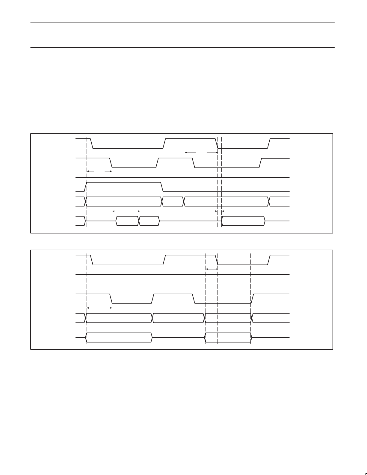
An access through the host interface starts when HIF CS_N = 0 and either HIF WR_N = 0 or HIF RD_N = 0. Typically the chip select signal is
derived from the upper address lines of the CPU (address decode stage), but it could also be connected to a port pin of the CPU to avoid the
need for an external address decoder in very simple CPU systems. When both HIF CS_N = 0 and HIF RD_N = 0 the host interface will start a
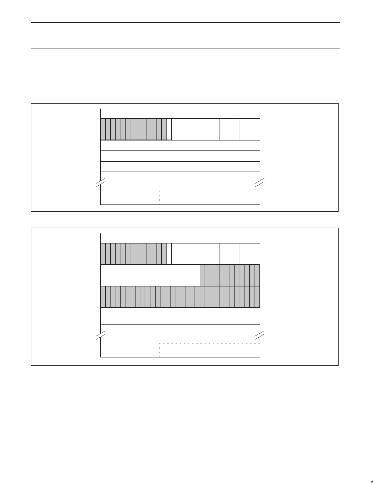
read access cycle, so the cycle is triggered at the falling edge of either HIF CS_N or HIF RD_N, whichever is later.
HIF CS_N
T
AS
HIF RD_N
T
HIF WR_N
HIF A8
AS
HIF A0..HIF A7
T
ACC
RSR
n
SV00686
HIF D0..HIF D7
T
ACC
RSR
RSR
O
n
Figure 4. Read cycle signal timing (2 independent read cycles)
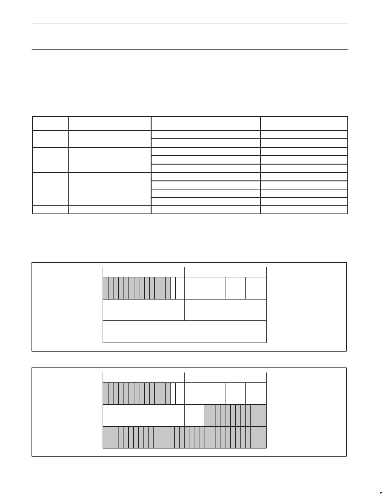
HIF CS_N
T
AS
HIF RD_N
HIF WR_N
T
AS
HIF A0..HIF A8
HIF D0..HIF D7
<VALID ADDRESS> <VALID ADDRESS>
<WRITE DATA> <WRITE DATA>
SV00687
Figure 5. Write cycle signal timing (2 independent write cycles)
12.4 The Asynchronous Packet Interface
The PDI1394L21 provides an interface to asynchronous data packets through the registers in the host interface. The format of the
asynchronous packets is specified in the following sections.
12.4.1 Reading an Asynchronous Packet
Upon reception of a packet, the packet data is stored in the appropriate receive FIFO, either the Request or Response FIFO. The location of the
packet is indicated by either the RREQQQAV or RRSPQAV status bit being set in the Asynchronous Interrupt Acknowledge (ASYINTACK)
register. The packet is transferred out of the FIFO by successive reads of the Asynchronous Receive Request (RREQ) or Asynchronous
Receive Response (RRSP) register. The end of the packet (the last quadlet) is indicated by either the RREQQLASTQ or RRSPQLASTQ bit set
in ASYINTACK. Attempting to read the FIFO when either RREQQQAV bit or RRSPQQAV bit is set to 0 (in the Asynchronous RX/TX interrupt
acknowledge (ASYINT ACK) register) will result in a queue read error.
1999 Aug 06
12
Philips Semiconductors Preliminary specification
1
No-packet data
3
Block Packet
PDI1394L211394 full duplex AV link layer controller
12.5 Link Packet Data Formats
The data formats for transmission and reception of data are shown below. The transmit format describes the expected organization for data
presented to the link at the asynchronous transmit, physical response, or isochronous transmit FIFO interfaces.
12.5.1 Asynchronous Transmit Packet Formats
These sections describe the formats in which packets need to be delivered to the queues (FIFOs) for transmission. There are four basic formats
as follows:
ITEM
FORMAT USAGE
p
Quadlet read requests 4
Quadlet/block write responses 2
TRANSACTION CODE
(tCode)
Quadlet write requests 0
2 Quadlet packet
Quadlet read responses 6
Block read requests 5
Block write requests 1
Block read responses 7
Lock requests 9
Lock responses B
4 Unformatted transmit Concatenated self-ID / PHY packets E
hex
hex
Each packet format uses several fields (see names and descriptions below). More information about these fields (not the format) can be found
in the 1394 specification. Grey fields are reserved and should be set to zero values.
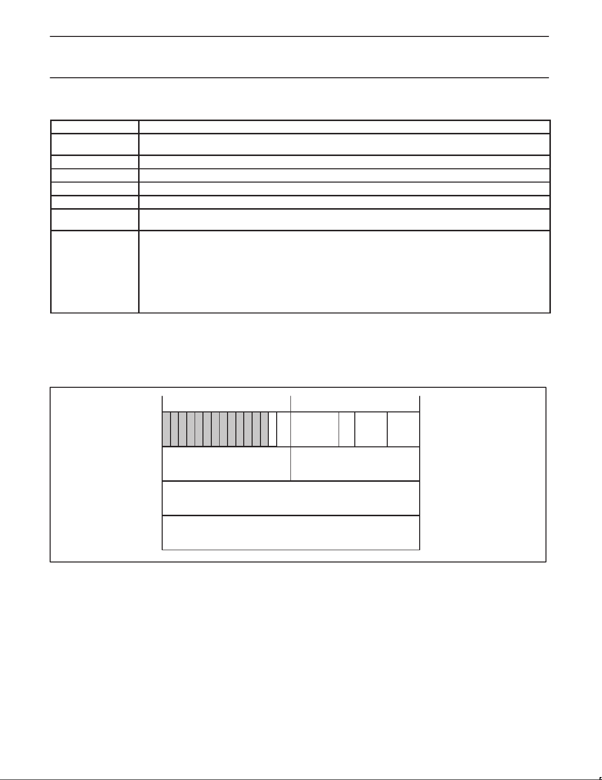
12.5.1.1 No-data Transmit
The no-data transmit formats are shown in Figures 6 and 7. The first quadlet contains packet control information. The second and third quadlets
contain 16-bit destination ID and either the 48-bit, quadlet aligned destination offset (for requests) or the response code (for responses).
31 30
29 28 27 2625 24 23 22 2120 19 18 17 16 15 14 13 12 11 10 9 8 7 6 5 4 3 2 1 0
0
spd tLabel rt tCode 0000
1999 Aug 06
destinationID
destinationOffsetLow
destinationOffsetHigh
Figure 6. Quadlet Read Request Transmit Format
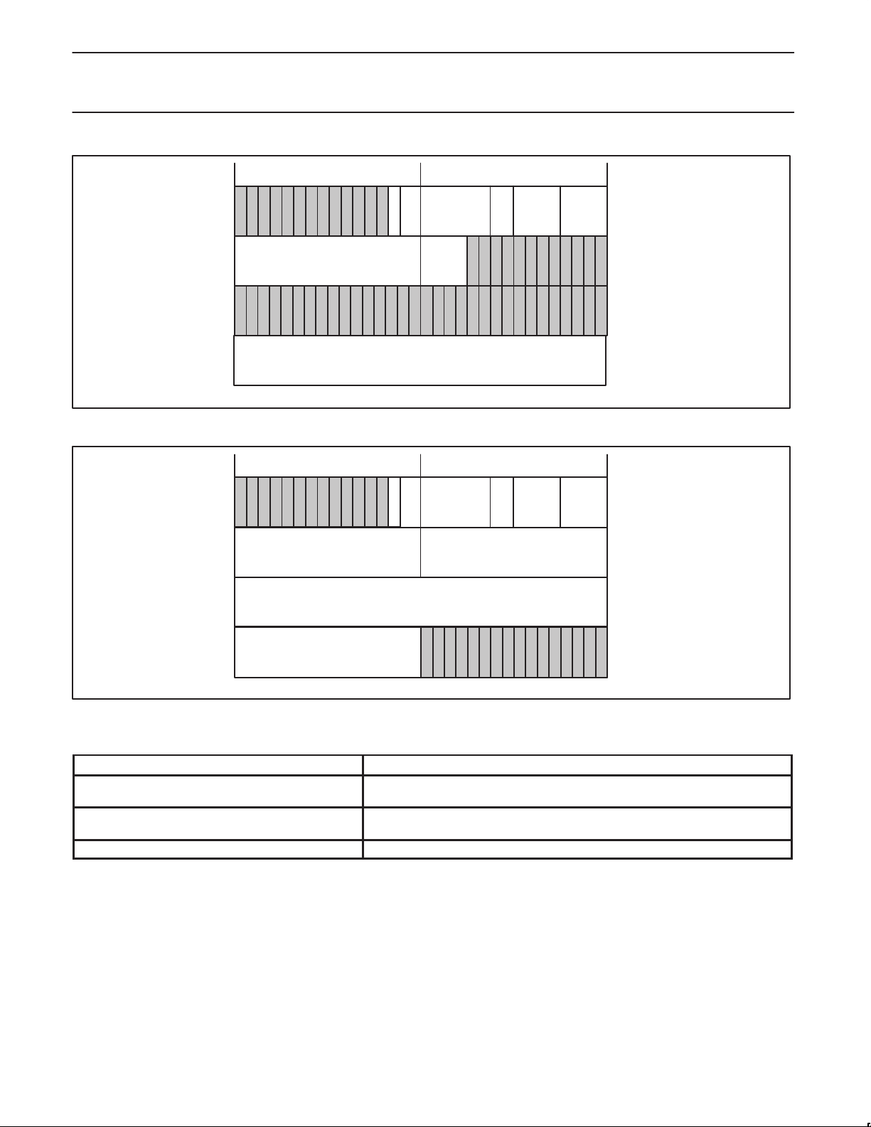
3130
29 28 27 2625 24 23 22 2120 19 18 17 16 15 14 13 12 11 10 9 8 7 6 5 4 3 2 1 0
spd tLabel rt tCode 0000
0
destinationID
rCode
Figure 7. Quadlet/Block Write Response Packet Transmit Format
13
SV00250
SV00249
Philips Semiconductors Preliminary specification
PDI1394L211394 full duplex AV link layer controller
Table 1. No-Data Transmit Format
Field Name Description
spd This field indicates the speed at which this packet is to be sent. 00=100 Mbs, 01=200 Mbs, and 10=400 Mbs.
tLabel This field is the transaction label, which is used to pair up a response packet with its corresponding request packet.
rt The retry code for this packet. Supported values are: 00=retry1, and 01=retryX.
tCode The transaction code for this packet.
DestinationID Contains a node ID value.
DestinationOffsetHigh
DestinationOffsetLow
rCode Response code for write response packet.
11 = undefined
The concatenation of these two field addresses a quadlet in the destination node’s address space.
rCode Meaning
0 Node successfully completed requested operation.
1–3 Reserved
4 Resource conflict detected by responding agent. Request may be retried.
5 Hardware error. Data not available.
6 Field within request packet header contains unsupported or invalid value.
7 Address location within specified node not accessible.
8–Fh Reserved
12.5.1.2 Quadlet Transmit
Three quadlet transmit formats are shown below. In these figures: The first quadlet contains packet control information. The second and third
quadlets contain 16-bit destination ID and either the 48-bit quadlet-aligned destination offset (for requests) or the response code (for responses).
The fourth quadlet contains the quadlet data for read response and write quadlet request formats, or the upper 16 bits contain the data length
for the block read request format.
29 28 27 2625 24 23 22 2120 19 18 17 16 15 14 13 12 11 10 9 8 7 6 5 4 3 2 1 0
3130
spd tLabel rt tCode 0000
0
destinationID
destinationOffsetLow
quadlet data
destinationOffsetHigh
SV00251
Figure 8. Quadlet Write Request T ransmit Format
1999 Aug 06
14
Philips Semiconductors Preliminary specification
PDI1394L211394 full duplex AV link layer controller
29 28 27 2625 24 23 22 2120 19 18 17 16 15 14 13 12 11 10 9 8 7 6 5 4 3 2 1 0
31 30
0
spd tLabel rt tCode 0000
destinationID
rCode
quadlet data
Figure 9. Quadlet Read Response Transmit Format
29 28 27 2625 24 23 22 2120 19 18 17 16 15 14 13 12 11 10 9 8 7 6 5 4 3 2 1 0
31 30
spd tLabel rt tCode 0000
0
destinationID
destinationOffsetLow
data length
destinationOffsetHigh
SV00252
SV00253
Figure 10. Block Read Request Transmit Format
Table 2. Quadlet Transmit Fields
Field Name Description
spd, tLabel, rt, tCode, destinationID,
destinationOffsetHigh, destinationOffsetLow, rCode
Quadlet data For quadlet write requests and quadlet read responses, this field holds the data to
Data length The number of bytes requested in a block read request.
1999 Aug 06
See Table 1.
be transferred.
15
Philips Semiconductors Preliminary specification
PDI1394L211394 full duplex AV link layer controller
12.5.1.3 Block Transmit
The block transmit format is shown below, this is the generic format for reads and writes. The first quadlet contains packet control information.
The second and third quadlets contain the 16-bit destination node ID and either the 48-bit destination offset (for requests) or the response code
and reserved data (for responses). The fourth quadlet contains the length of the data field and the extended transaction code (all zeros except
for lock transaction). The block data, if any, follows the extended transaction code.
29 28 27 2625 24 23 22 2120 19 18 17 16 15 14 13 12 11 10 9 8 7 6 5 4 3 2 1 0
31 30
spd tLabel rt tCode 0000
0
destinationID
destinationOffsetLow
dataLength extendedTcode
Block data
destinationOffsetHigh
padding (if needed)
Figure 11. Block Packet Transmit Format
29 28 27 2625 24 23 22 2120 19 18 17 16 15 14 13 12 11 10 9 8 7 6 5 4 3 2 1 0
31 30
spd tLabel rt tCode 0000
0
destinationID rCode
dataLength extendedTcode
SV00254
1999 Aug 06
Block data
padding (if needed)
SV00255
Figure 12. Block Read or Lock Response Transmit Format
16
 Loading...