

Philips PDI1394L Service Manual

PDI1394L11
1394 AV link layer controller
Preliminary specification 1996 Nov 06
INTEGRATED CIRCUITS
Philips Semiconductors Preliminary specification
PDI1394L111394 AV link layer controller
2
1996 Nov 06
1.0 FEATURES
•IEEE 1394–1995 Standard Link Layer Controller
•Hardware Support for the Proposed IEC1883 Standard of Digital
Interface for Consumer Electronics
•Interfaces to any IEEE 1394–1995 Physical Layer Interfaces
•5V Tolerant I/Os
•Single 3.3V supply voltage
2.0 DESCRIPTION
The PDI1394L11, Philips Semiconductors 1394 Audio/Video (AV)
Link Layer Controller, is an IEEE 1394–1995 compliant link layer
controller featuring an embedded AV layer interface. The AV layer is
designed to pack and un–pack application data packets for
transmission over an IEEE 1394 bus using isochronous data
transfers.
The application data is packetized according to the proposed IEC
1883 Specification of Digital Interface for Consumer Electronic
Audio/Video Equipment. The AV layer interface is a byte–wide port
capable of accommodating various MPEG–2 and DVC codecs. An
80C51 or MC68XX compatible byte–wide host interface is provided
for internal register configuration as well as performing
asynchronous data transfers.
The PDI1394L11 is powered by a single 3.3V power supply and the
inputs and outputs are 5V tolerant. It is available in the PQFP80
package.
3.0 QUICK REFERENCE DATA
GND = 0V; T
amb
= 25°C; tr =tf 2.5 ns
SYMBOL
PARAMETER CONDITIONS MIN TYP MAX UNIT
V
DD
Functional supply voltage range 3.0 3.3 3.6 V
I
DD
Total supply current @ VDD=3.3V TBD mA
SCLK Device clock 0 49.978 50 MHz
4.0 ORDERING INFORMATION
PACKAGES TEMPERATURE RANGE OUTSIDE NORTH AMERICA NORTH AMERICA PKG. DWG. #
80-pin plastic PQF80 0°C to +70°C PDI1394L11 D PDI1394L11 D SOT318–2
Philips Semiconductors Preliminary specification
PDI1394L111394 AV link layer controller
1996 Nov 06
3
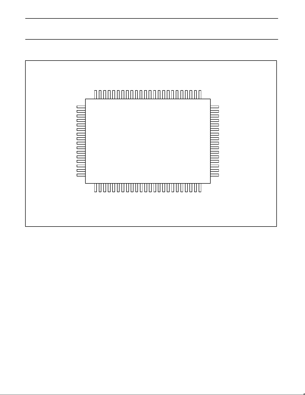
5.0 PIN CONFIGURATION
PDI1394L11
AV LINK LAYER CONTROLLER
RESERVED PHY D3
RESERVED
AV D7
RESERVED
VDD
CYCLEOUT
AV D4
PHY D7
AV D0
AV D1
AV D3
AV D2
VDD
GND
AV D5
AV D6
VDD_
GND
N/C
VDD
GND
PHY D4
PHY D5
GND
CYCLEIN
RESET_N
HIF INT _N
HIF RD_N
HIF WR_N
HIF CS_N
PHY D6
GND
AVSYNC
N/C
VDD
AVFSYNCOUT
AVFSYNCIN
AVVALID
AVCLK
SCLK
LREQ
AVENDPCK
AVERR0
N/C
GND
AVERR1
VDD
HIF D6
HIF D2
HIF D5
HIF D7
GND
VDD
HIF D4
HIF D3
HIF D0
RESERVED
HIF D1
GND
HIF A8
HIF A7
VDD
HIF A6
31
30
32
29
27
26
28
25
66
57
65
58
70
71
59
72
74
75
73
76
78
79
77
80
63
62
64
61
59
58
60
57
55
54
56
53
515052
49
2
3
1
4
6
7
5
8
10
11
9
12
141513
16
SV00270
VDD
GND
18
202119
222423
47
46
48
45
43
42
44
41
17
HIF A4
HIF A3
HIF A5
HIF A2
HIF A0
HIF A1
39
38
40
37
35
34
36
33
PHY CTL0
PHY CTL1
ISO_N
VDD
PHY D0
PHY D1
GND
PHY D2
Philips Semiconductors Preliminary specification
PDI1394L111394 AV link layer controller
1996 Nov 06
4
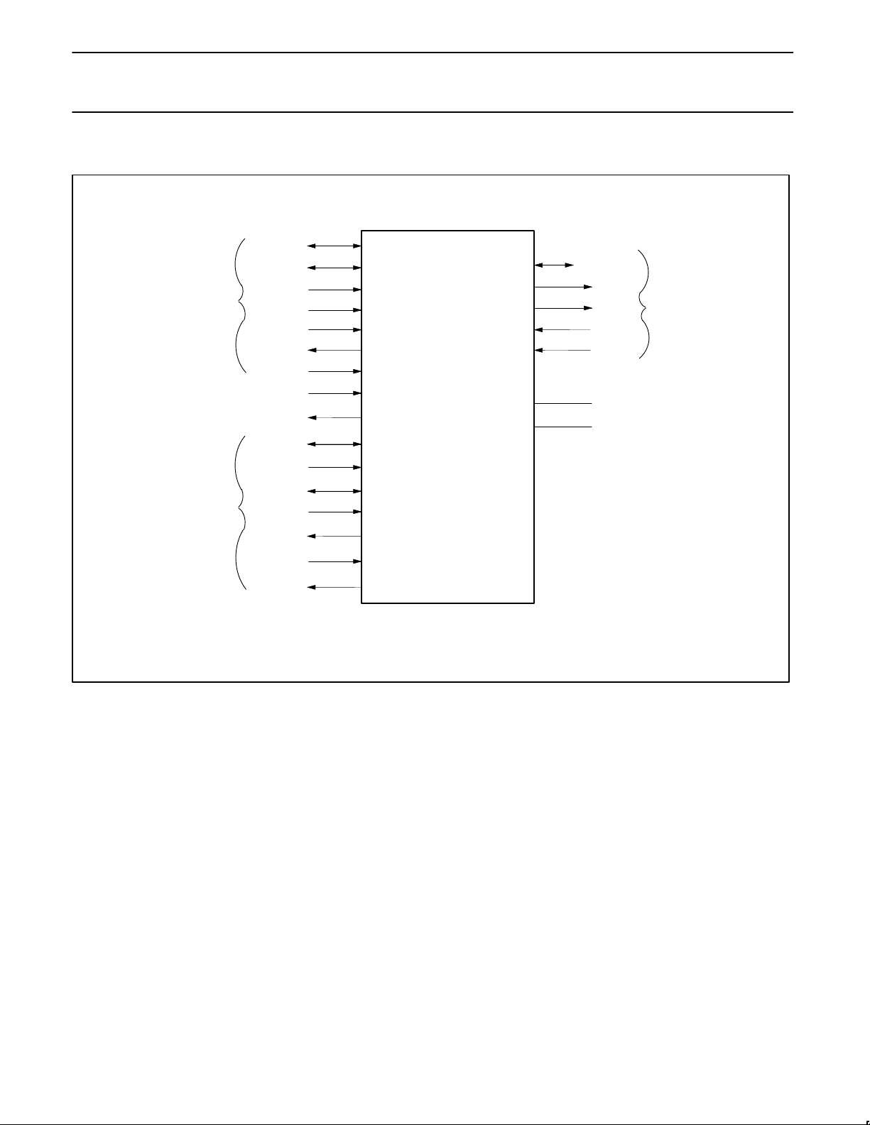
6.0 FUNCTIONAL DIAGRAM
AV LAYER
SV00267
HOST
PHY
HIF A[8:0]
HIF D[7:0]
HIF WR_N
HIF RD_N
HIF CS_N
HIF INT_N
RESET_N
CYCLEIN
CYCLEOUT
AV D[7:0]
AVCLK
AVSYNC
AFSYNCIN
AVFSYNCOUT
AVENDPCK
AVERR[1:0]
PHY D[0:7]
CTL0
LREQ
ISO_N
SCLK
VDD
GND
PDI1394L11
IEEE 1394
AV LINK LAYER CONTROLLER
Philips Semiconductors Preliminary specification
PDI1394L111394 AV link layer controller
1996 Nov 06
5
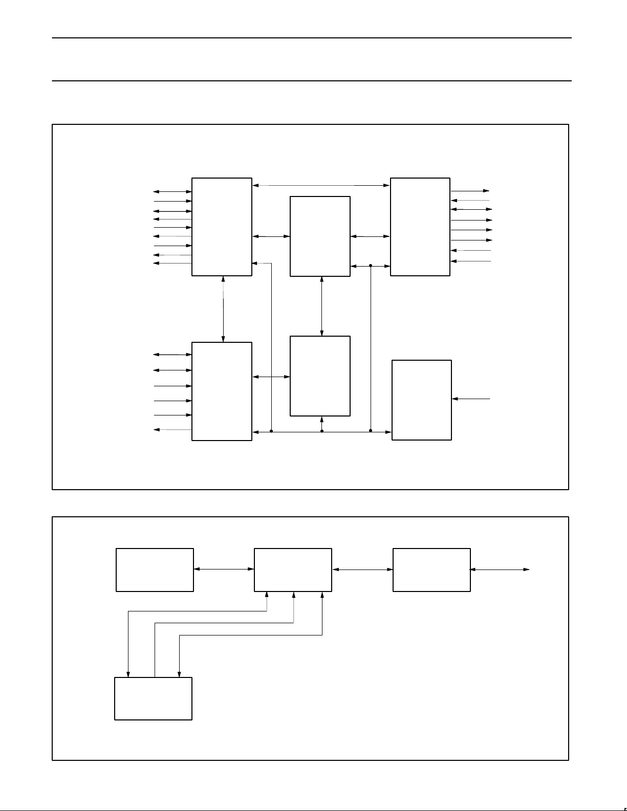
7.0 INTERNAL BLOCK DIAGRAM
HIF A[8:0]
HIF D[7:0]
HIF WR_N
HIF RD_N
HIF CS_N
HIF INT_N
RESET_N
CYCLEIN
CYCLEOUT
AV DATA[7:0]
AVCLK
AVSYNC
AFSYNCIN
AVFSYNCOUT
AVENDPCK
AVERR1
PHY D[0:7]
CTL0
LREQ
ISO_N
SCLK
SV00269
AVERR0
AVVALID
CTL1
AV LAYER
TRANSMITTER
AND
RECEIVER
5KB
BUFFER
MEMORY
(ISOC & ASYNC
PACKETS)
LINK CORE
8-BIT
INTERFACE
ASYNC
TRANSMITTER
AND
RECEIVER
CONTROL
AND
STATUS
REGISTERS
8.0 APPLICATION DIAGRAM
SAA7201
MPEG DECODER
PDI1394L11
AV LINK
AV
INTERFACE
PDI1394P11
PHY
PHY–LINK
INTERFACE
8051
HOST CONTROLLER
DATA 8/
ADDRESS 9/
INTERRUPT & CONTROL
1394 CABLE
INTERFACE
SV00268

Philips Semiconductors Preliminary specification
PDI1394L111394 AV link layer controller
1996 Nov 06
6
9.0 PIN DESCRIPTION
9.1 Host Interface
PIN No. PIN SYMBOL I/O NAME AND FUNCTION
14, 15, 16, 17,
18, 19, 20, 21, 22
HIF A[8:0] I
Host Interface Address 0 through 8. Provides the host with a byte wide interface to internal
registers. See description of Host Interface for addressing rules.
1, 2, 3, 4, 7, 8, 9,
10
HIF D[7:0] I/O Host Interface Data 7 (MSB) through 0. Byte wide data path to internal registers.
26 HIF WR_N I
Write enable. When asserted (LOW) in conjunction with HIF CS_N, a write to the PDI1394L1 1
internal registers is requested.
27 HIF RD_N I
Read enable. When asserted (LOW) in conjunction with HIF CS_N, a read of the PDI1394L11
internal registers is requested.
25 HIF CS_N I
Chip Select (active LOW). Host bus control signal to enable access to the FIFO and control
and status registers.
28 HIF INT_N O
Interrupt (active low). Indicates a interrupt internal to the PDI1394L11. Read the General
Interrupt Register for more information.
29 RESET_N I Reset (active low). The asynchronous master reset to the PDI1394L11.
30 CYCLEIN I
Provides the capability to supply an external cycle timer signal for the beginning of 1394 bus
cycles.
33 CYCLEOUT O Reproduces the 8kHz cycle clock of the cycle master.
6, 13, 24, 32, 39,
45, 49, 64, 72, 78
V
DD
3.0V " 0.3V power supply
5, 12, 23, 31, 38,
44, 50, 63, 73, 79
GND Ground reference
9.2 AV Interface
PIN No. PIN SYMBOL I/O NAME AND FUNCTION
77, 76, 75, 74,
71, 70, 69, 68
AVDATA[7:0] I/O Audio/Video Data 7 (MSB) through 0. Byte–wide interface to the AV layer.
58 AVCLK I External application clock. Rising edge active.
57 AVSYNC I/O Start of packet indicator.
59 AVFSYNCIN I Frame sync input, rising edge active.
60 AVFSYNCOUT O Frame sync output
56 AVENDPCK I
End of application packet indication from data source. Indicates input packet is not multiple of
DBS.
61 AVVALID I/O Indicates data on AVDATA is valid
53 AVERR0 O CRC error, indicates bus packet containing AVDATA had a CRC error.
52 AVERR1 O
Sequence Error. Indicates at least one source packet was lost before the current source
packet.
9.3 Phy Interface
PIN No. PIN SYMBOL I/O NAME AND FUNCTION
34, 35, 36, 37,
40, 41, 42, 43
PHY D[7:0] I/O
Data 0 (MSB) through 7 (NOTE: To preserve compatibility to the specified Link–Phy interface
of the IEEE 1394–1995 specification, bit 0 is the most significant bit). Data is expected on
D[0:1] for 100Mb/s, D[0:3] for 200Mb/s, and D[0:7] for 400Mb/s. See 1394 Specification for
more information.
46, 47 PHY CTL[1:0] I/O Control Lines between Link and Phy. See 1394 Specification for more information.
48 ISO_N I
Isolation barrier. This terminal is asserted (low) when an isolation barrier is present. See 1394
Specification for more information.
54 LREQ O Link Request. Bus request to access the PHY. See 1394 Specification for more information.
55 SCLK I System clock. 49.152MHz input from the PHY. Used to generate a 24.576MHz clock.
9.4 Other Pins
PIN No. PIN SYMBOL I/O NAME AND FUNCTION
65, 66, 67 RESERVED NA
These pins are reserved for factory testing. For normal operation they should be connected to
ground.
11, 51, 62, 80 N/C NA These pins are should be not be connected or terminated.

Philips Semiconductors Preliminary specification
PDI1394L111394 AV link layer controller
1996 Nov 06
7
10.0 RECOMMENDED OPERATING CONDITIONS
LIMITS
SYMBOL
PARAMETER
CONDITIONS
UNIT
MIN.
MAX.
V
CC
DC supply voltage 3.0 3.6 V
V
I
Input voltage 0 5 V
V
IH
High-level input voltage 2.0 V
V
IL
Low-level input voltage 0.8 V
I
OH
High-level output current 8 mA
I
OL
Low-level output current –8 mA
dT/dV Input transition rise or fall time 0 20 ns/V
T
amb
Operating ambient temperature range 0 +70 °C
SCLK System clock 49.1519 49.1521 MHz
AVCLK AV interface clock
11.0 ABSOLUTE MAXIMUM RATINGS
1, 2
In accordance with the Absolute Maximum Rating System (IEC 134). Voltages are referenced to GND (ground = 0V)
LIMITS
SYMBOL
PARAMETER
CONDITIONS
MIN MAX
UNIT
V
DD
DC supply voltage –0.5 +4.6 V
I
IK
DC input diode current – –50 mA
V
I
DC input voltage –0.5 +5.5 V
I
OK
DC output diode current – " 50 mA
V
O
DC output voltage –0.5 VDD +0.5 V
I
O
DC output source or sink current – " 50 mA
I
GND
, ICCDC VCC or GND current – " 150 mA
T
stg
Storage temperature range –60 150 °C
T
amb
Operating ambient temperature 0 70 °C
P
tot
Power dissipation per package TBD W
NOTES:
1. Stresses beyond those listed may cause permanent damage to the device. These are stress ratings only and functional operation of the
device at these or any other conditions beyond those indicated under “recommended operating conditions” is not implied. Exposure to
absolute-maximum-rated conditions for extended periods may affect device reliability.
2. The performance capability of a high-performance integrated circuit in conjunction with its thermal environment can create junction
temperatures which are detrimental to reliability. The maximum junction temperature of this integrated circuit should not exceed 150°C.
11.1 Buffer Memory Sizes
BUFFER MEMORY
SIZE
(Quadlets)
Asynchronous Receive Transaction Response FIFO 64
Asynchronous Receive Transaction Request FIFO 64
Asynchronous Transmit Transaction Response FIFO 64
Asynchronous Transmit Transaction Request FIFO 64
AV Transmit/Receive Buffer 1024

Philips Semiconductors Preliminary specification
PDI1394L111394 AV link layer controller
1996 Nov 06
8
12.0 FUNCTIONAL DESCRIPTION
12.1 Overview
The PDI1394L11 is an IEEE 1394–1995 compliant link layer controller. It provides a direct interface between a 1394 bus and various MPEG–2
and DVC codecs. Via this interface, the AV Link maps and un–maps these AV datastreams from the these codecs onto 1394 isochronous bus
packets. The AV Link also provides an 8051 / MC68XX compatible interface for an attached host controller. Through the host interface port, the
host controller can configure the AV layer for transmission or reception of AV datastreams. The host interface port also allows the host
controller to transmit and receive 1394 asynchronous data packets.
12.2 AV interface and AV layer
The AV interface and AV layer allow AV packets to be transmitted from one node to another. The AV transmitter and receiver with in the AV
layer perform all the functions required to pack and unpack AV packet data for transfer over a 1394 network. Once the AV layer is properly
configured for operation, no host controller service should be required. The host controller will have to intervene only in the case of an AV
transmit/receive buffer overrun, or other error event in the AV layer. The operation of the AV layer is half–duplex, i.e., an AV layer can either
receive or transmit AV packets at a particular time.
12.2.1 The AV Interface
The AV Link provides an 8 bit data path to the AV layer. The 8 bit data path is designed with associated clock and control signals to be
compatible with various MPEG–2 and DVC codecs.
When properly configured, the AV interface port will time stamp and buffer the incoming AV packets. The AV packet data is stored in the
embedded memory buffer, along with its time stamp information. During the next available isochronous bus cycle, the AV layer creates an
isochronous bus packet with the appropriate CIP header and AV data. The size and configuration of isochronous data packet payload
transmitted is determined by the AV layer’s configuration registers accessible through the host interface.
Once configured, the AV interface port waits for the assertion of AVVALID and AVSYNC as well as a valid AVCLK. AVSYNC is a pulse that is
aligned with the leading edge of AVCLK and the first byte of data on AVDATA[7:0]. Its duration is one AVCLK cycle. AVSYNC signals the AV
layer that the transfer of an AV packet has begun. At the time that AVSYNC is asserted, the AV layer stores the current time stamp in the buffer
memory. This time stamp is transmitted, as part of the standard packet header, to signal the receiver at what time to provide the AV packet for
output. As long as AVVALID is asserted, the data byte data present on AV DATA[7:0] at the active edge of AVCLK will be clocked into the AV
layer for processing.
At the end of the AV data packet, assertion of AVENDPCK, for one clock, will signal the AV layer that the packet is complete. This signal is
usually used when the AV packet does not fulfill the AV packet size used in the AV layer configuration.
12.2.2 IEC1883
The PDI1394L11 is specifically designed to support the proposed IEC1883 Specifications of Digital Interface for Consumer Electronic
Audio/Video Equipment. The IEC specification defines a scheme for mapping various types of AV datastreams onto 1394 isochronous data
packets. The specification also defines a software protocol for managing isochronous channels in a 1394 network called Function Control
Protocol (FCP) and Connection Management Procedures (CMP).
The mapping of AV datastreams onto 1394 isochronous packets is handled automatically by the AV Link. A special ‘AV layer’ is included in the
AV Link to manage the packing and unpacking of AV datastreams onto isochronous packets. Some features of the AV layer are automatic
time–stamping of incoming packets, buffer memory management and automatic construction of 1394 isochronous packets. Each 1394
isochronous packet generated by the AV layer contains a special header holding information specific to the packing parameters used to make
the packet. These special headers are called Common Isochronous Packet (CIP) headers.
12.2.3 CIP Headers
A feature of the IEC1883 specification is the definition of Common Isochronous Packet (CIP) headers. These CIP headers contain information
about the source and type of datastream mapped onto the isochronous packets.
The AV Layer supports the use of CIP headers. CIP headers are added to transmitted isochronous data packets at the AV data source. When
receiving isochronous data packets, the AV layer automatically analyzes their CIP headers. The analysis of the CIP headers determines the
method the AV layer uses to unpack the AV data from the isochronous data packets.
The information contained in the CIP headers is accessible via registers in the host interface.
(See proposed IEC1883 ”Specifications of Digital Interface for Consumer Electronic Audio/Video Equipment” December 1995, Section 6 for
more details on CIP headers).

Philips Semiconductors Preliminary specification
PDI1394L111394 AV link layer controller
1996 Nov 06
9
12.3 Host interface Port
The PDI1394L11 Host interface provides an 8 bit (bytewide) data path, 9 address lines, and associated control lines to access the AV Link
Controller’s 32–bit internal registers. The interfacing scheme allows the bytewide data path to access the internal registers in 4 accesses.
12.3.1 Using the Host Interface
The PDI1394L11 Host interface provides an 8 bit (bytewide) data path, 9 address lines, and assorted control lines to access the AV Link
Controller’s 32–bit internal registers. The interfacing scheme allows the bytewide data path to access the internal registers in 4 accesses.
12.3.2 Addressing Scheme
The PDI1394L11 contains twenty–nine (29) 32–bit internal registers. These registers are accessible through the 8–bit host interface data path
using a quadlet–to–byte multiplexing scheme. The multiplexing scheme involves reading or writing the contents of an internal register to a
shadow register. The shadow register provides the host interface with access to the internal register’s contents, one byte at a Tinsmith. The
host interface contains a 32–bit shadow register that is used to temporarily store internal register data during reads or writes. Host interface
Address bit 8 (HIF ADDR8) is used to signal internal logic to either transfer the contents of an internal 32–bit register to the host interface
shadow register, in the case of a read, or transfer the contents of the host interface shadow register to an internal 32–bit register, in the case of
a write. Reading the shadow register with HIF A8=1 is called a read with update, writing to the shadow register with HIF A8=1 is called a write
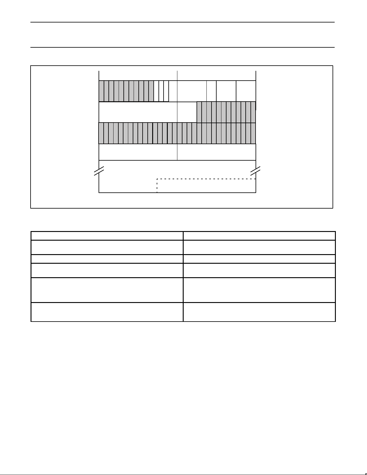
with update. Successive reads to the other 3 bytes of the 32–bit register should not have HIF A8 set. An example of accessing the General
Control Register is shown in Figure 1.
The host interface uses 9 address bits to form the bytewide addresses. Each internal 32–bit register has a base address that points to the
lowest order byte in the register. The next three addresses (base address+1, +2, and +3) are the next higher order bytes of the 32–bit internal
register. Note that base address+0 retrieves or writes the most significant byte, bits 31–24, of a 32–bit register; base address+1 retrieves or
writes the next most significant byte, bits 23–16 of a 32–bit register; and so on.
**********************
This code segment shows how to read the General Control Register, located at address 0x004 and move its contents to an array
located at TEMP.
**********************
MOVE 0x104, TEMP Gets contents of GENCTL bits 31–24, low byte, and moves it to TEMP
MOVE 0x005, TEMP+1 Gets the next byte of GENCTL bits 23–16 and moves it to TEMP+1
MOVE 0x006, TEMP+2 Gets the 3rd byte of GENCTL bits 15–8 and moves it to TEMP+2
MOVE 0x007, TEMP+3 Gets the last byte of GENCTL bits 7–0 and moves it to TEMP+3
**********************
This code segment shows how to write the General Control Register, located at address 0x004 with the contents of an array
located at TEMP.
**********************
MOVE TEMP, 0x004 Moves TEMP to the first byte of GENCTL, bits 31–24
MOVE TEMP+1,0x005 Moves TEMP+1 to the second byte of GENCTL, bits 23–16
MOVE TEMP+2, 0x006 Moves TEMP+2 to the 3rd byte of GENCTL, bits 15–8
MOVE TEMP+3, 0x107 Moves TEMP+3 to the last byte of GENCTL, bits 7–0, and performs the write with update
SV00266
Figure 1. General Control Register Read/Write Code Segments
Philips Semiconductors Preliminary specification
PDI1394L111394 AV link layer controller
1996 Nov 06
10
12.4 The Asynchronous Packet Interface
The PDI1394L11 provides an interface to asynchronous data packets through the registers in the host interface. The format of the
asynchronous packets is specified in the following sections.
12.4.1 Reading an Asynchronous Packet
Upon reception of a packet, the packet data is stored in the appropriate receive FIFO, either the Request or Response FIFO. The location of
the packet is indicated by either the RXRQA or RXRPA status bit being set in the Asynchronous RX/TX Control 2 (ASY_CR2) register. The
packet is transferred out of the FIFO by successive reads of the Asynchronous Receive Request (RX_RQ) or Asynchronous Receive Response
(RX_RP) register. The end of the packet (the last quadlet) is indicated by either the RXRPL or RXRQL bit set in ASY_CR2. Continuing to try to
read the FIFO after the last quadlet has been read will result in a queue read error indicated by the either RXRQE bit or RXRPE bit being set in
Asynchronous RX/TX Control 2 (ASY_CR2) register.
12.4.2 Writing an Asynchronous Packet
An asynchronous packet intended for transmission is first stored in the appropriate Transmitter FIFO. Once writing to the FIFO is complete, the
link layer controller arbitrates for the bus to transmit the packet.
To generate an asynchronous packet, the first and next to last quadlets of the packet must be written to the Asynchronous Transmit Request
Nextone (TX_RQ_NEXT) register, for request type packets, or the Asynchronous Transmit Response Next (TX_RP_NEXT) register, for
response type packets. The last quadlet of the packet is written to the Asynchronous Transmit Request Last (TX_RQ_LAST) register, for
request type packets, or the Asynchronous Transmit Response Last (TX_RP_LAST) register, for response type packets. After writing the last
quadlet, the packet is automatically queued by the AVlink layer controller for transmission over the bus.
12.5 Link Packet Data Formats
The data formats for transmission and reception of data are shown below. The transmit format describes the expected organization for data
presented to the link at the asynchronous transmit, physical response, or isochronous transmit FIFO interfaces. The receive format of data link
presents at the receive FIFO interface.
12.5.1 Asynchronous Transmit
There are four basic formats for asynchronous data to be transmitted:
1. no–data packets (used for quadlet read requests and all write responses)
2. quadlet packets (used for quadlet write requests, quadlet read responses, and block read requests)
3. block packets (used for lock requests and responses, block write requests, and block read responses)
4. unformatted data.
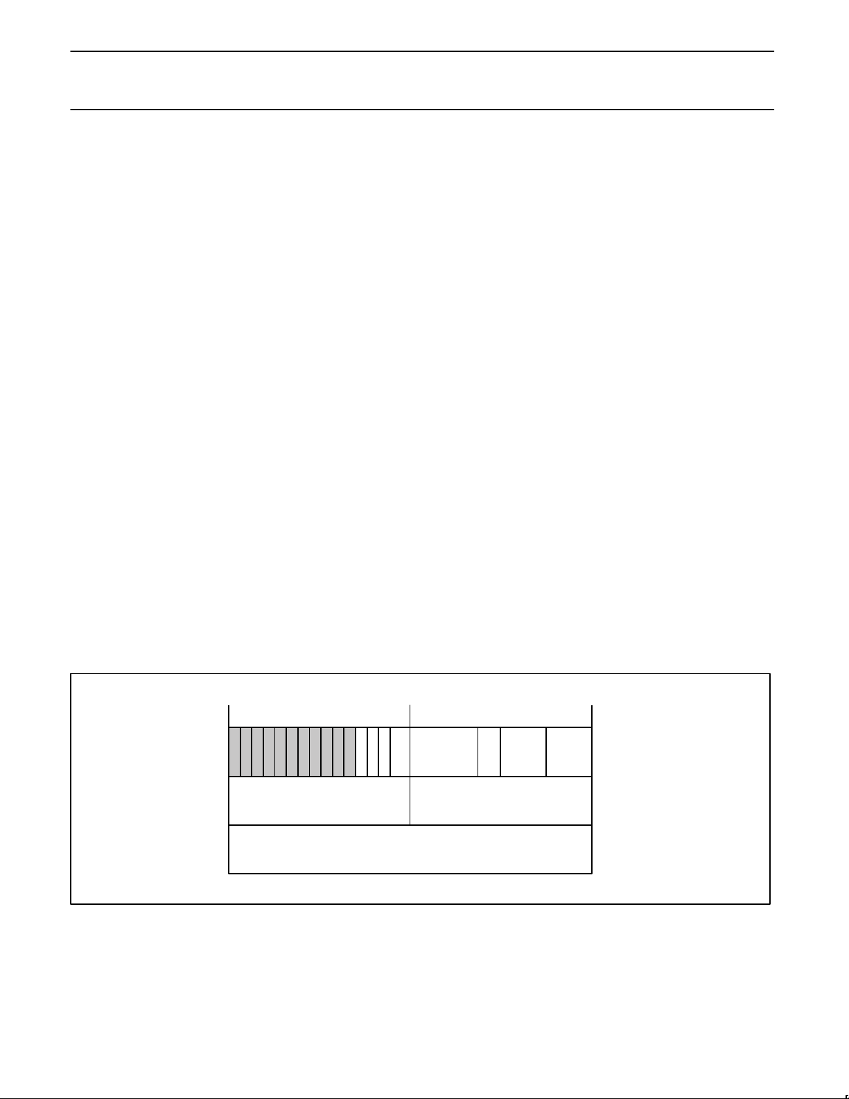
12.5.1.1 No–data Transmit
The no–data transmit format is shown in Table 1. The first quadlet contains packet control information. The second and third quadlets contain
16–bit destination ID and either the 48–bit, quadlet aligned destination offset(for requests) or the response code (for responses).
destinationID
spd tLabel rt
tCode priority
imm
enable AT
31
30
29 28 27 2625
24 23 22 212019 18 1716
15 141312
1110 987 6 5 4 3 2 1 0
destinationOffsetHigh
SV00250
destinationOffsetLow
Figure 2. Quadlet Read Request Tansmit Format
Philips Semiconductors Preliminary specification
PDI1394L111394 AV link layer controller
1996 Nov 06
11
destinationID
spd tLabel rt
tCode priority
imm
enable AT
SV00249
31
30
29 28 27 2625
24 23 22 212019 18 1716
15 141312
1110 987 6 5 4 3 2 1 0
rCode
Figure 3. Write Response Transmit Format
Table 1. No-Data Transmit Format
Field Name Description
enableAT Re–enable asynchronous transmit operation. After a bus reset, all asynchronous transmit packets are flushed until
a packet header with this bit is set is presented. Important: this bit should only be set for a single packet after a bus
reset is detected. Normally this bit should be cleared, allowing the link core to flush queued packets that may no
longer be correctly addressed after a bus reset.
imm Always set to $0’.
spd This field indicates the speed at which this packet is to be sent. 00=100 Mbs, 01=200 Mbs, and 10=400 Mbs.
11 = undefined
tLABEL This field is the transaction label, which is used to pair up a response packet with its corresponding request
packet.
rt The retry code for this packet. 00=retry 1, 01=retryX, 10=retryA, 11=retryB
tCode The transaction code for this packet.
Priority The priority level for this packet. Any non–zero value directs the transmitter to use priority arbitration for this
packet.
DestinationID This is the concatenation of the 10–bit bus address and the 6–bit node number for the destination of this packet.
DestinationOffsetHigh
DestinationOffsetLow
The concatenation of these two field addresses a quadlet in the destination node’s address space. This address
must be quadlet–aligned (modulo 4).
RCode Response code for write response packet.
Philips Semiconductors Preliminary specification
PDI1394L111394 AV link layer controller
1996 Nov 06
12
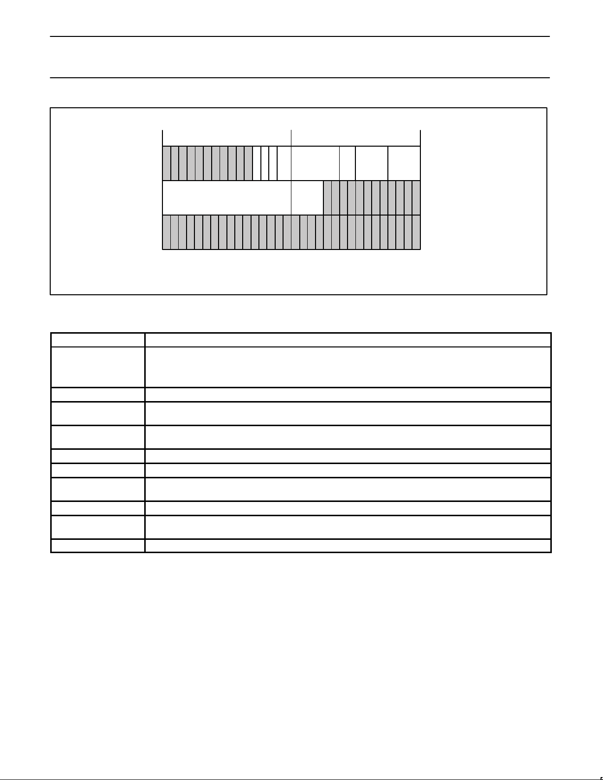
12.5.1.2 Quadlet Transmit
Three quadlet transmit formats are shown below. In these figures: The first quadlet contains packet control information. The second and third
quadlets contain 16–bit destination ID and either the 48–bit quadlet–aligned destination offset (for requests) or the response code (for
responses).
The fourth quadlet contains the quadlet data for read response and write quadlet request formats, or the upper 16 bits contain the data length
for the block read request format.
destinationID
spd tLabel rt
tCode priority
imm
enable AT
31
30
29 28 27 2625
24 23 22 212019 18 1716
15 141312
1110 987 6 5 4 3 2 1 0
destinationOffsetHigh
destinationOffsetLow
quadlet data
SV00251
Figure 4. Quadlet Write Request Transmit Format
destinationID
spd tLabel rt
tCode priority
imm
enable AT
31
30
29 28 27 2625
24 23 22 212019 18 1716
15 141312
1110 987 6 5 4 3 2 1 0
rCode
quadlet data
SV00252
Figure 5. Quadlet Read Request Transmit Format
Philips Semiconductors Preliminary specification
PDI1394L111394 AV link layer controller
1996 Nov 06
13
destinationID
spd tLabel rt
tCode priority
imm
enable AT
31
30
29 28 27 2625
24 23 22 212019 18 1716
15 141312
1110 987 6 5 4 3 2 1 0
destinationOffsetHigh
destinationOffsetLow
data length
SV00253
Figure 6. Block Read Request Transmit Format
Table 2. Quadlet Transmit Fields
Field Name Description
enableAT, imm, spd, tLabel, rt, tCode, priority, destinationID,
destinationOffsetHigh, destinationOffsetLow, rCode
See Table 1
Quadlet data For quadlets write requests and quadlet read responses, this field
holds the data to be transferred
Data length The number of bytes requested in a block read request
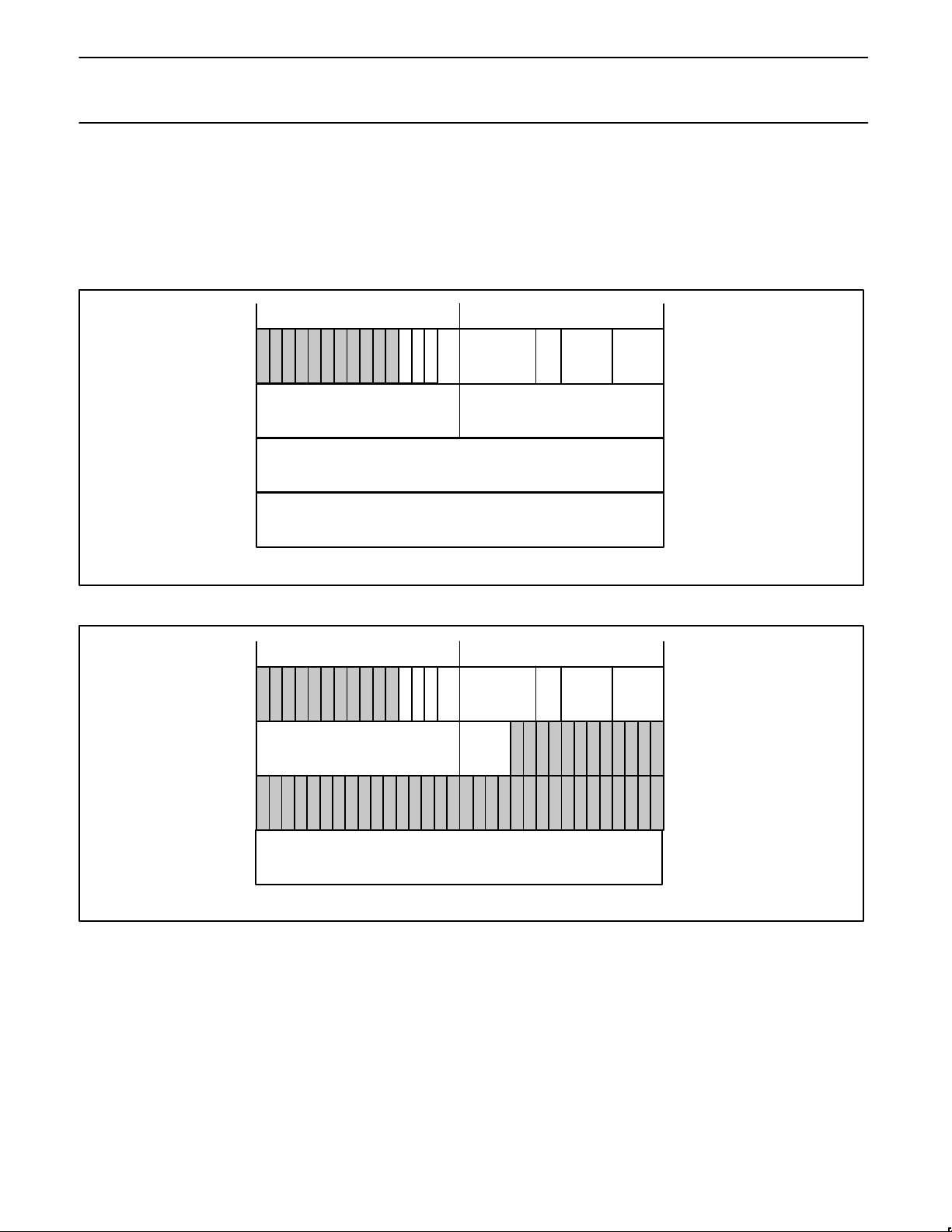
12.5.1.3 Block Transmit
The block transmit format is shown below, this is the generic format for reads and writes. The first quadlet contains packet control information.
The second and third quadlets contain the 16–bit destination node ID and either the 48–bit destination offset (for requests) or the response code
and reserved data (for responses). The fourth quadlet contains the length of the data field and the extended transaction code (all zeros except
for lock transaction). The block data, if any, follows the extended code.
destinationID
spd tLabel rt
tCode priority
imm
enable AT
31
30
29 28 27 2625
24 23 22 212019 18 1716
15 141312
1110 987 6 5 4 3 2 1 0
destinationOffsetHigh
destinationOffsetLow
dataLength extendedTcode
Block Length
padding (if needed)
SV00254
Figure 7. Block Transmit Format
Philips Semiconductors Preliminary specification
PDI1394L111394 AV link layer controller
1996 Nov 06
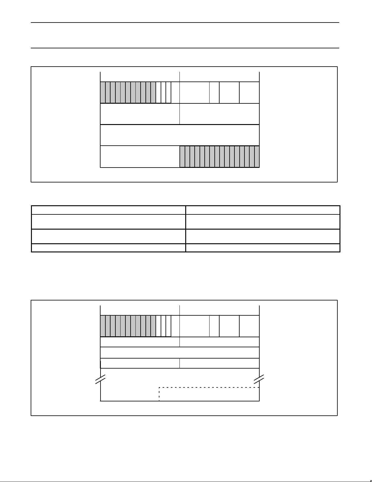
14
spd tLabel rt
tCode priority
imm
enable AT
31
30
29 28 27 2625
24 23 22 212019 18 1716
15 141312
1110 987 6 5 4 3 2 1 0
dataLength extendedTcode
Block Length
padding (if needed)
SV00255
destinationID
rCode
Figure 8. Block Read or Lock Response Transmit Format
Table 3. Block Transmit Field
Field Name Description
enableAT, imm, spd, tLabel, rt, tCode, priority, destinationID,
destinationOffsetHigh, destinationOffsetLow, rCode
See Table 2.
dataLength The number of bytes of data to be transmitted in this packet
extendedTcode The tCode indicates a lock transaction, this specifies the actual lock
action to be performed with the data in this packet.
block data The data to be sent. If dataLength=0, no data should be written into
the FIFO for this field. Regardless of the destination or source
alignment of the data, the first byte of the block must appear in the
high order byte of the first quadlet.
padding If the dataLength mod 4 is not zero, then zero–value bytes are added
onto the end of the packet to guarantee that a whole number of
quadlets is sent.
 Loading...