

Philips PDI1284P11DGG, PDI1284P11DL Datasheet

INTEGRATED CIRCUITS
PDI1284P11
3.3V Parallel interface transceiver/buffer
Product specification
Supersedes data of 1997 Sep 15
1999 Sep 17
Philips Semiconductors Product specification
PDI1284P1 13.3V Parallel interface transceiver/buffer
FEA TURES
•Asynchronous operation
•8-Bit transceivers
•6 additional buffer/driver lines peripheral to cable
•5 additional control lines from cable
•5V tolerant
•ESD protection exceeds 2000V per MIL STD 883 Method 3015
and 200V per Machine Model
•Latch up protection exceeds 500 mA per JEDEC Std 19
•Input Hysteresis
•Low Noise Operation
DESCRIPTION
The PDI1284P1 1 parallel interface chip is designed to provide an
asynchronous, 8-bit, bi-directional, parallel interface for personal
computers. The part includes all 19 signal lines defined by the
IEEE1284 interface specification for Byte, Nibble, EPP, and ECP
modes. The part is designed for hosts or peripherals operating at
3.3V to interface 3.3V or 5.0V devices.
The 8 transceiver pairs (A/B 1-8) allow data transmission from the A
bus to the B bus, or from the B bus to the A bus, depending on the
state of the direction pin DIR.
The B bus and the Y9-Y13 lines have either totem pole or resistor
pull up outputs, depending on the state of the high drive enable pin
HD. The A bus has only totem pole style outputs. All inputs are TTL
compatible with at least 400mV of input hysteresis at V
•IEEE 1284 Compliant Level 1 & 2
•Overvoltage Protection on B/Y side for OFF-state
•A side 3-State option
•B side active or resistive pull up option
•Cable side V
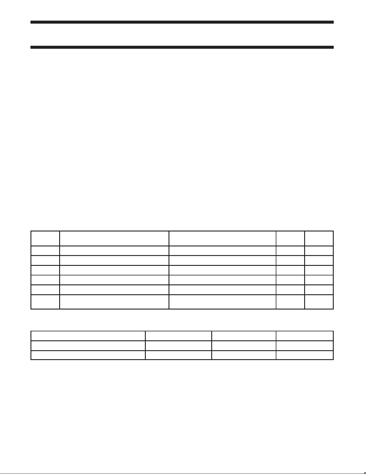
QUICK REFERENCE DATA
SYMBOL PARAMETER
R
D
R
PU
SR B/Y Side slew rate RL = 62Ω; CL = 50pF (See Waveform 4) 0.2 V/ns
I
CC
V
HYS
t
PLH/tPHL
A –B/Y
for 5V or 3V operation
CC
CONDITIONS
T
= 25°C; GND = 0V
amb
B/Y Side output resistance VCC = 3.3V; VO = 1.65V ±0.2V (See Figure 2) 45 Ω
B/Y side pull up resistance VCC = 3.3V; Outputs, resistive pull up 1.4K Ω
Total static current VI = VCC/GND; IO = 0 5 µA
Input hysteresis VCC= 3.3V 0.47 V
Propagation delay
to the B/Y side outputs
VCC = 3.3V 12.5/13.9 ns
TYPICAL UNIT
= 3.3V.
CC
ORDERING INFORMATION
PACKAGES TEMPERATURE RANGE ORDER CODE DRAWING NUMBER
48-pin plastic SSOP Type II 0°C to +70°C PDI1284P1 1 DL SOT370-1
48-pin plastic TSSOP Type II 0°C to +70°C PDI1284P11 DGG SOT362-1
1999 Sep 17 853–2036 22356
2
Philips Semiconductors Product specification
PDI1284P113.3V Parallel interface transceiver/buffer
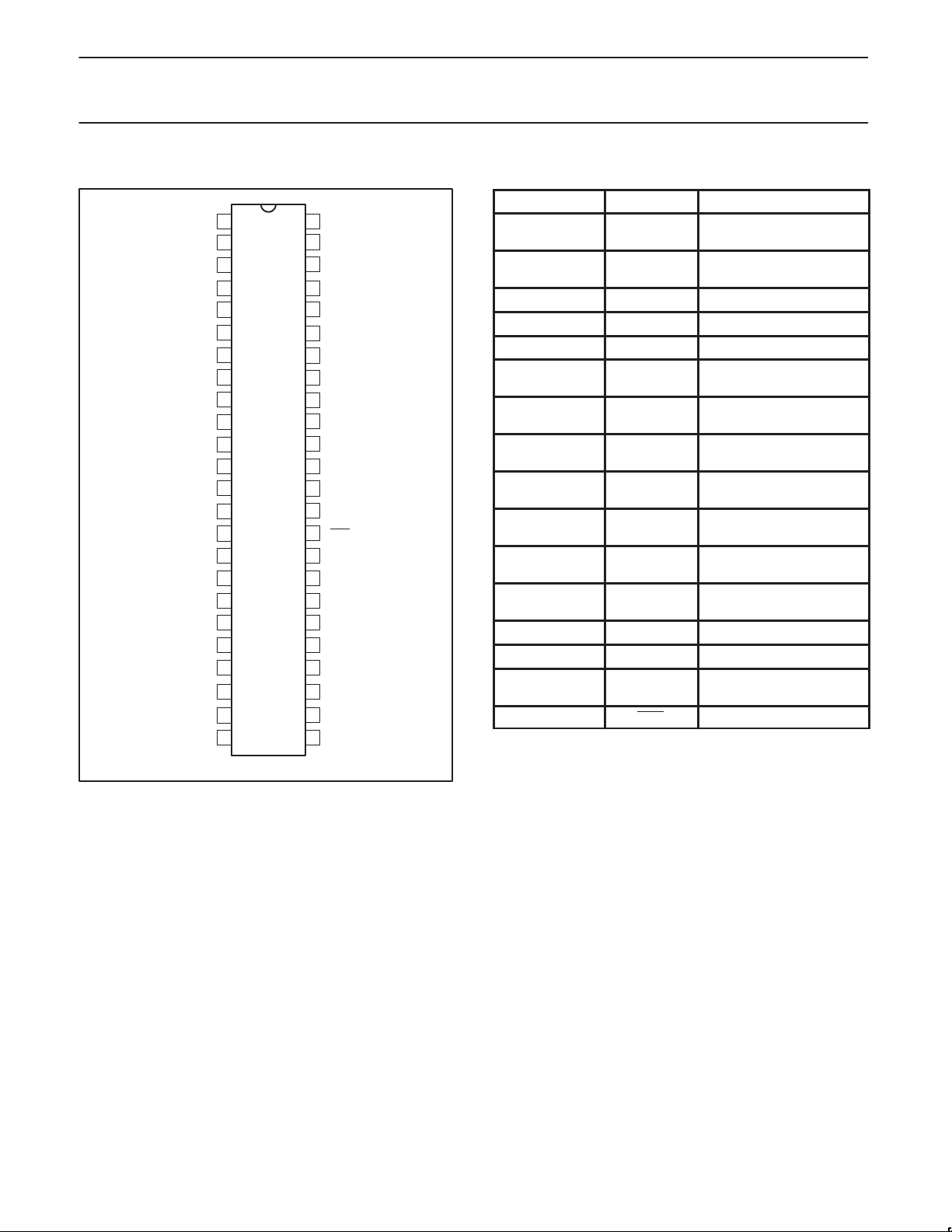
PIN CONFIGURATION
1
HD
2
A9
3
A10
4
A11
5
A12
6
A13
7
V
CC
8
A1
9
A2
10
GND
11
A3
12
A4
13
A5
14
A6
15
GND
16
A7
A8
17
18
V
CC
19
PLHI
20
A14
21
A15
22
A16
23
A17
24
HLHO
PIN DESCRIPTION
PIN NUMBER SYMBOL FUNCTION
DIR
48
47
Y9
46
Y10
Y11
45
44
Y12
Y13
43
V
42
CCB
B1
41
B2
40
39
GND
38
B3
37
B4
36
B5
35
B6
34
OEA
33
B7
32
B8
31
V
CCB
30
PLHO
C14
29
C15
28
C16
27
26
C17
25
HLHI
8, 9, 11, 12, 13,
14, 16, 17
41, 40, 38, 37,
36, 35, 33, 32
A1 - A8 Data inputs/outputs
B1 - B8
IEEE 1284 Std.
outputs/inputs
2, 3, 4, 5, 6 A9 - A13 Data inputs
47, 46, 45, 44, 43 Y9 - Y3 IEEE 1284 Std. outputs
29, 28, 27, 26 C14 - C17 Control inputs (cable)
20, 21, 22, 23 A19 - A17
1 HD
48 DIR
19 PLHI
30 PLHO
25 HLHI
24 HLHO
Control outputs
(peripheral)
B/Y–side high drive
enable/disable
Direction selection
A to B / B to A
Peripheral logic high input
(peripheral)
Peripheral logic high
output (cable)
Host logic high input
(cable)
Host logic high output
(cable)
10, 15, 39 GND Ground (0V)
7, 18 V
31, 42 V
CC
CCB
Positive supply voltage
Cable side power supply
voltage 3V/5V
34 OEA A side output enable
1999 Sep 17
SV00496
3

Philips Semiconductors Product specification
PDI1284P113.3V Parallel interface transceiver/buffer
LOGIC SYMBOL
HD
A9
A10
A11
A12
A13
A1
A2
A3
A4
A5
A6
A7
A8
PLHI
CNTL
CNTL
CNTL
CNTL
CNTL
CNTL
CNTL
CNTL
HD
HD
HD
HD
HD
HD
HD
HD
HD
HD
HD
HD
HD
HD
HD
CNTL
DIR
OEA
Y9
Y10
Y11
Y12
Y13
B1
B2
B3
B4
B5
B6
B7
B8
PLHO
FUNCTION TABLE
DIR OEA HD INPUTS OUTPUTS
X X X C14-17 A14-17 t
X X X HLHI HLHO t
X X L A9-13 Y9-13 r
X X H A9-13 Y9-13 t
X X L PLHI PLHO O.C.
X X H PLHI PLHO t
H X L A1-8 B1-8 r
H X H A1-8 B1-8 t
L L X B1-8 A1-8 t
L H X A1-8 Z*
L H X B1-8 r
A = Side driving internal IC
B = Side driving external cable (bidirectional)
C = Side receiving control signals from internal cable
Y = Side driving external cable (unidirectional)
X = Don’t care – control signals in
Z = High Z or 3-State
O.C.= Open collector
= Totem pole output
t
P
r
= Resistive pull up: 1.4kΩ (nominal) on B/Y/C cable side and
P
* When DIR = L and OEA
. However, while a B/Y side output is Low as driven by a
V
CC
Low signal on the A side, that particular B/Y side resistor is
switched out to stop current drain from V
= H, the output signal is isolated
through it.
CC
from the input signal. B1 – 8 signals maintain an r
on the input for this mode.
OUTPUT
TYPES
P
P
P
P
P
P
P
P
P*
= 1.4kΩ
P
A14
A15
A16
A17
HLHO
PERIPHERAL
SIDE
C14
C15
C16
C17
HLHI
CABLE
SIDE
SV00136
PINS WITH PUL L UP RESISTORS TO LOAD CABLE
PINS SYMBOL FUNCTION
47, 46, 45, 44, 43 Y9 – Y13 Output cable drivers
41, 40, 38, 37, 36,
35, 33, 32
29, 28, 27, 26 C14 – C17
B1 – B8 Output cable drivers
External cables control signal
input
1999 Sep 17
4
 Loading...