

Philips PCK2509S Datasheet

INTEGRATED CIRCUITS
PCK2509S
50–150 MHz 1:9 SDRAM clock driver
Product specification 1999 Oct 19
Philips Semiconductors Product specification
PCK2509S50–150 MHz 1:9 SDRAM clock driver
FEA TURES
•Phase-Locked Loop Clock distribution for PC100/PC133 SDRAM
applications
•Spread Spectrum clock compatible
•Operating frequency 50 to 150 MHz
•(t
phase error
– jitter) at 100 to133 MHz = ±50 ps
•Jitter (peak-peak) at 100 to 133 MHz = ± 80 ps
•Jitter (cycle-cycle) at 100 to 133 MHz = 65 ps
•Pin-to-pin skew < 200 ps
•Available in plastic 24-Pin TSSOP
•Distributes one clock input to one bank of ten outputs
•External Feedback (FBIN) terminal Is used to synchronize the
outputs to the clock input
•On-Chip series damping resistors
•No external RC network required
•Operates at 3.3 V
•Inputs compatible with 2.5 V and 3.3 V ranges
DESCRIPTION
The PCK2509S is a high-performance, low-skew, low-jitter,
phase-locked loop (PLL) clock driver. It uses a PLLto precisely align,
in both frequency and phase, the feedback (FBOUT) output to the
clock (CLK) input signal. It is specifically designed for use with
synchronous DRAMs. The PCK2509S operates at 3.3 V V
input compatible with both 2.5 V and 3.3 V input voltage ranges. It
also provides integrated series-damping resistors that make it ideal
for driving point-to-point loads.
One bank of five outputs and one bank of four outputs provide nine
low-skew, low-jitter copies of CLK. Output signal duty cycles are
CC
and is
adjusted to 50 percent, independent of the duty cycle at CLK. Each
bank of outputs can be enabled or disabled separately via the
control (1G and 2G) inputs. When the G inputs are high, the outputs
switch in phase and frequency with CLK; when the G inputs are low,
the outputs are disabled to the logic–low state.
Unlike many products containing PLLs, the PCK2509S does not
require external RC networks. The loop filter for the PLL is included
on-chip, minimizing component count, board space, and cost.
Because it is based on PLL circuitry, the PCK2509S requires a
stabilization time to achieve phase lock of the feedback signal to the
reference signal. This stabilization time is required, following power up
and application of a fixed-frequency, fixed-phase signal at CLK, and
following any changes to the PLL reference or feedback signals. The
PLL can be bypassed for test purposes by strapping AV
to ground.
CC
The PCK2509S is characterized for operation from 0°C to +70°C.
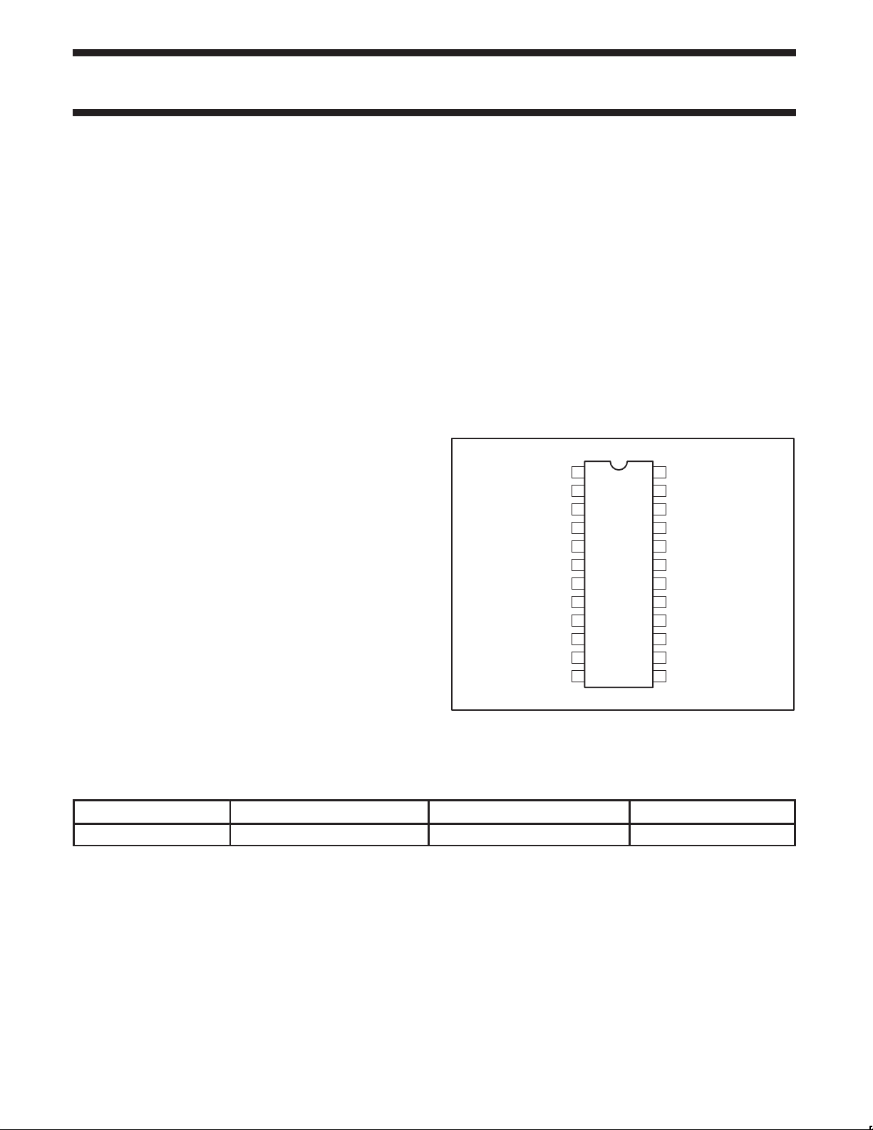
PIN CONFIGURATION
1
AGND
2
V
CC
3
1Y0
4
1Y1
5
1Y2
6
GND
7
GND
8
1Y3
9
1Y4
10
V
CC
11
1G
12 13
FBOUT
CLK
24
23
AV
22
V
CC
21
2Y0
20
2Y1
19
GND
18
GND
17
2Y2
16
2Y3
V
15
CC
14
2G
FBIN
SW00389
CC
ORDERING INFORMA TION
PACKAGES TEMPERATURE RANGE ORDER CODE DRAWING NUMBER
24-Pin Plastic TSSOP 0°C to +70°C PCK2509S PW SOT355-1
1999 Oct 19 853–2180 22544
2
Philips Semiconductors Product specification
PCK2509S50–150 MHz 1:9 SDRAM clock driver
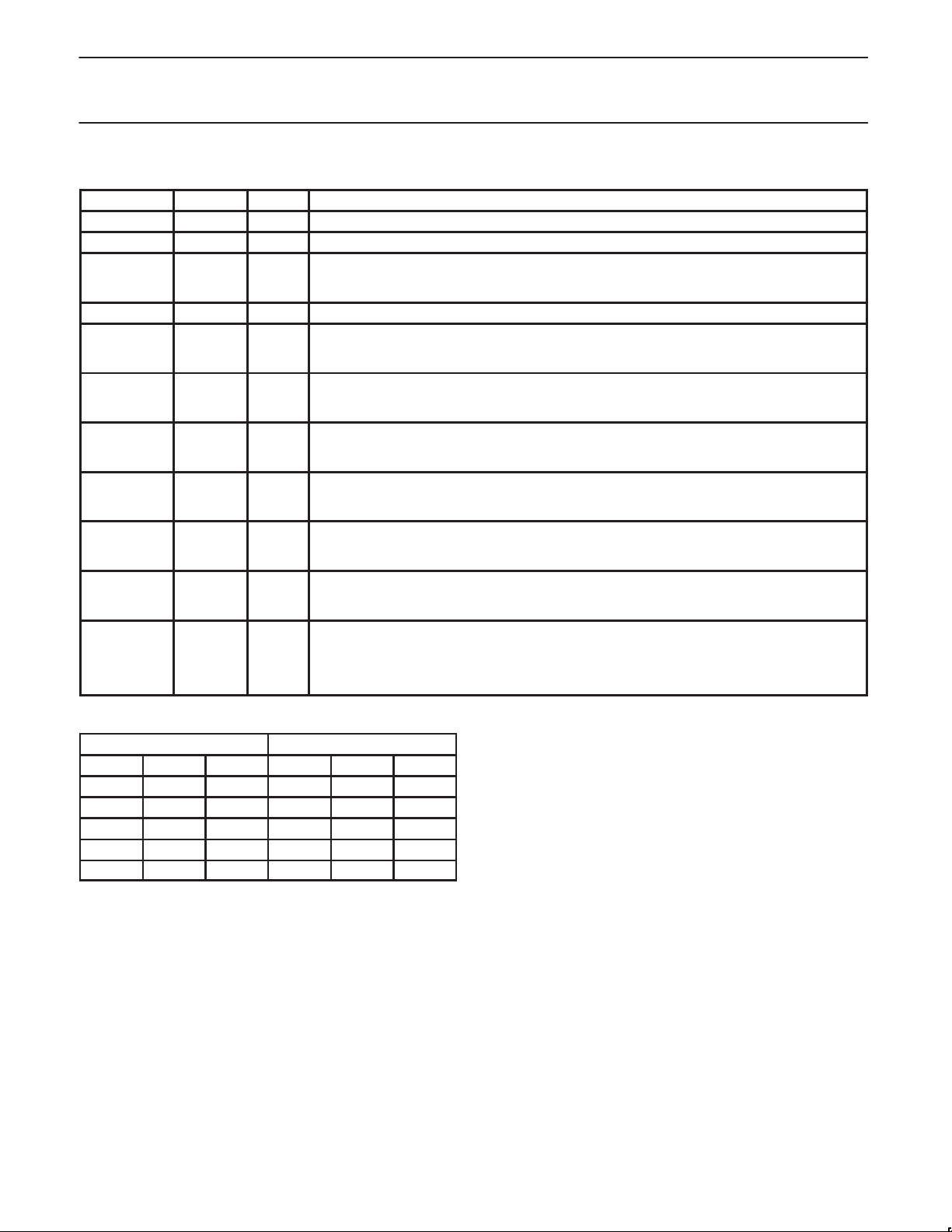
PIN DESCRIPTIONS
PIN NUMBER SYMBOL TYPE NAME, FUNCTION, and DIRECTION
1 AGND GND Analog ground. AGND provides the ground reference for the analog circuitry.
2, 10, 15, 22 V
3, 4, 5, 8, 9 1Y (0–4) OUT
6, 7, 18, 19 GND GND Ground
11 1G IN
12 FBOUT OUT
13 FBIN IN
14 2G IN
16, 17, 20, 21 2Y (0–3) OUT
23 AV
24 CLK IN
CC
CC
PWR Power supply
Clock outputs. These outputs provide low-skew copies of CLK. Output bank 1Y(0–4) is enabled
via the1G input. These outputs can be disabled to a logic LOW state by de-asserting the 1G control
input. Each output has an integrated 25 Ω series-damping resistor.
Output bank enable. 1G is the output enable for outputs 1Y(0–4). When 1G is LOW, outputs
1Y(0–4) are disabled to a logic LOW state. When 1G is HIGH, all outputs 1Y(0–4) are enabled and
switch at the same frequency as CLK.
Feedback output. FBOUT is dedicated for external feedback. It switches at the same frequency as
CLK. When externally wired to FBIN, FBOUT completes the feedback loop of the PLL. FBOUT has
an integrated 25 Ω series-damping resistor.
Feedback input. FBIN provides the feedback signal to the internal PLL. FBIN must be hard-wired
to FBOUT to complete the PLL. The integrated PLL synchronizes CLK and FBIN so that there is
nominally zero phase error between CLK and FBIN.
Output bank enable. 2G is the output enable for outputs 2Y(0–3). When 2G is LOW, outputs
2Y(0–3) are disabled to a logic LOW state. When 2G is HIGH, all outputs 2Y(0–3) are enabled and
switch at the same frequency as CLK.
Clock outputs. These outputs provide low-skew copies of CLK. Output bank 2Y(0–3) is enabled
via the 2G input. These outputs can be disabled to a logic LOW state by de-asserting the 2G
control input. Each output has an integrated 25 Ω series-damping resistor.
Analog power supply. AVCC provides the power reference for the analog circuitry. In addition,
PWR
AVCC can be used to bypass the PLL for test purposes. When AVCC is strapped to ground, PLL is
bypassed and CLK is buffered directly to the device outputs.
Clock input. CLK provides the clock signal to be distributed by the PCK2509S clock driver. CLK is
used to provide the reference signal to the integrated PLL that generates the clock output signals.
CLK must have a fixed frequency and fixed phase for the PLL to obtain phase lock. Once the circuit
is powered up and a valid CLK signal is applied, a stabilization time is required for the PLL to phase
lock the feedback signal to its reference signal.
FUNCTION TABLE
INPUTS OUTPUTS
1G 2G CLK 1Y (0–4) 2Y (0–3) FBOUT
X X L L L L
L L H L L H
L H H L H H
H L H H L H
H H H H H H
1999 Oct 19
3
 Loading...