

Philips PCK2010RDL Datasheet

INTEGRATED CIRCUITS
PCK2010R
CK98R (100/133MHz) RCC spread
spectrum system clock generator
Product specification
Supersedes data of 1999 Oct 19
2000 May 17
Philips Semiconductors Product specification
CK98R (100/133MHz) RCC spread spectrum
system clock generator
FEA TURES
•Mixed 2.5 V and 3.3 V operation
•Four CPU clocks at 2.5 V
•Eight PCI clocks at 3.3 V, one free-running
(synchronous with CPU clocks)
•Four 3.3 V fixed clocks @ 66 MHz
•Two 2.5 V CPUDIV2 clocks @ ½ CPU clock frequency
•Three 2.5 V IOAPIC clocks @ 16.67 MHz
•One 3.3 V 48 MHz USB clock
•Two 3.3 V reference clocks @ 14.318 MHz
•Reference 14.31818 MHz Xtal oscillator input
•133 MHz or 100 MHz operation
•Power management control input pins
•CPU clock jitter ≤ 250 ps cycle-cycle
•CPU clock skew ≤ 175 ps pin-pin
•0.0ns – 1.5 ns CPU - 3V66 delay
•1.5ns – 3.5 ns 3V66 - PCI delay
•1.5ns – 4.0 ns CPU - IOAPIC delay
•1.5ns – 4.0 ns CPU - PCI delay
•Available in 56-pin SSOP package
•±0.5% center spread spectrum capability via select pins
•–0.5% down spread spectrum capability via select pins
DESCRIPTION
The PCK2010R is a clock generator (frequency synthesizer) chip for
a Pentium II and other similar processors.
The PCK2010R has four CPU clock outputs at 2.5 V, two CPUDIV2
clock outputs running at ½ CPU clock frequency (66 MHz or 50 MHz
depending on the state of SEL133/100) and four 3V66 clocks
running at 66MHz. There are eight PCI clock outputs running at
33 MHz. One of the PCI clock outputs is free-running. Additionally,
the part has three 2.5 V IOAPIC clock outputs at 16.67 MHz and two
3.3 V reference clock outputs at 14.318 MHz. All clock outputs meet
Intel’s drive strength, rise/fall time, jitter , accuracy, and skew
requirements.
The part possesses dedicated power-down, CPUSTOP
PCISTOP
input pins for power management control. These inputs
are synchronized on-chip and ensure glitch-free output transitions.
When the CPUSTOP input is asserted, the CPU clock outputs and
3V66 clock outputs are driven LOW. When the PCISTOP
asserted, the PCI clock outputs are driven LOW.
, and
input is
Finally, when the PWRDWN input pin is asserted, the internal
reference oscillator and PLLs are shut down, and all outputs are
driven LOW.
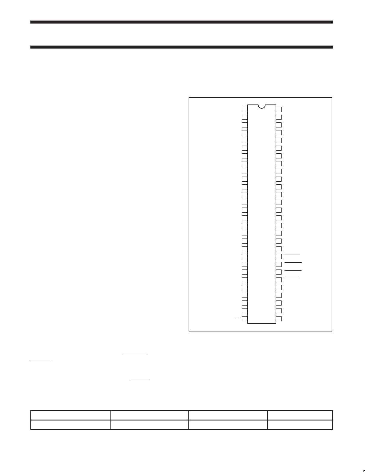
PIN CONFIGURATION
REF0
REF1
V
DD
XTAL_IN
XTAL_OUT
V
PCICLK_F
PCICLK1
V
DD
PCICLK2
PCICLK3
PCICLK4
PCICLK5
VDD3V
PCICLK6
PCICLK7
V
3V66_0
3V66_1
VDD3V
V
3V66_0
3V66_1
VDD3V
1
SS
2
3
4
3V
5
6
7
SS
8
9
10
3V
11
12 45
13
SS
14
15
16
17
18 39
19 38V
SS
20
SS
21
22
23
24
SS
25 32
26 31
27 30
28 29SEl133/100
PCK2010R
56V
V
25V
DD
55
APIC2
54
APIC1
APIC0
53
52
V
SS
51
25V
V
DD
50
CPUDIV2_1
CPUDIV2_0
49
48
V
SS
VDD25V
47
CPUCLK3
46
CPUCLK2
V
44V
SS
VDD25V
43
CPUCLK1
42
CPUCLK0
41
V
40
SS
3V
V
DD
V
SS
PCISTOP
37
CPUSTOP
36
35
PWRDWN
SPREAD
34
SEL1
33
SEL0
VDD3V
48MHz_USB
V
SS
SW00504
ORDERING INFORMA TION
PACKAGES TEMPERATURE RANGE ORDER CODE DRAWING NUMBER
56-Pin plastic SSOP 0°C to +70°C PCK2010R DL SOT371-1
Intel and Pentium are registered trademarks of Intel Corporation.
2000 May 17 853–2179 23685
2
Philips Semiconductors Product specification
CK98R (100/133MHz) RCC spread spectrum
PCK2010R
system clock generator
PIN DESCRIPTION
PIN NUMBER SYMBOL FUNCTION
2,3 REF [0–1] 3.3 V 14.318 MHz clock output
5 XTAL_IN 14.318 MHz crystal input
6 XTAL_OUT 14.318 MHz crystal output
8 PCICLK_F 3.3 V free running PCI clock
9, 11, 12, 14, 15, 17, 18 PCICLK [1–7] 3.3 V PCI clock outputs
21, 22, 25, 26 3V66 [0–3] 3.3 V fixed 66 MHz clock outputs
28 SEL133/100
30 48 MHz USB 3.3 V fixed 48 MHZ clock output
32, 33 SEL [0–1] Logic select pins. TTL levels.
34 SPREAD 3.3 V LVTTL input. Enables spread spectrum mode when held LOW.
35 PWRDWN 3.3 V LVTTL input. Device enters powerdown mode when held LOW.
36 CPUST OP
37 PCISTOP 3.3 V LVTTL input. Stops all PCI clocks except PCICLK_F when held LOW.
41, 42, 45, 46 CPUCLK [0–3] 2.5 V CPU output. 133 MHz or 100MHz depending on state of input pin SEL133/100.
49, 50 CPUDIV_2 [0–1]
53, 54, 55 IOAPIC [0–2]
4, 10, 16, 23, 27, 31, 39 V
1, 7, 13, 19, 20, 24, 29,
38, 40, 44, 48, 52
43, 47, 51, 56 V
NOTE:
1. V
, V
DD3V
on the performance of the device. In reality, the platform will be configured with the V
tied to a common 3.3 V supply and all V
and VSS in the above tables reflects a likely internal POWER and GROUND partition to reduce the effects of internal noise
DD25V
DD3V
V
SS
DD25V
pins being common.
SS
Select input pin for enabling 133 MHz or 100 MHz CPU outputs.
H = 133 MHz, L = 100 MHz
3.3 V LVTTL input. Stops all CPU clocks and 3V66 clocks when held LOW. CPUDIV_2
output remains on all the time.
2.5 V output running at 1/2 CPU clock frequency. 66 MHz or 50 MHz depending on
state of input pin SEL133/100.
2.5 V clock outputs running divide synchronous with the CPU clock frequency. Fixed
16.67 MHz limit.
3.3 V power supply.
Ground
2.5 V power supply
pins tied to a 2.5 V supply, all remaining V
DD25V
DD
pins
2000 May 17
3
Philips Semiconductors Product specification
CK98R (100/133MHz) RCC spread spectrum
system clock generator
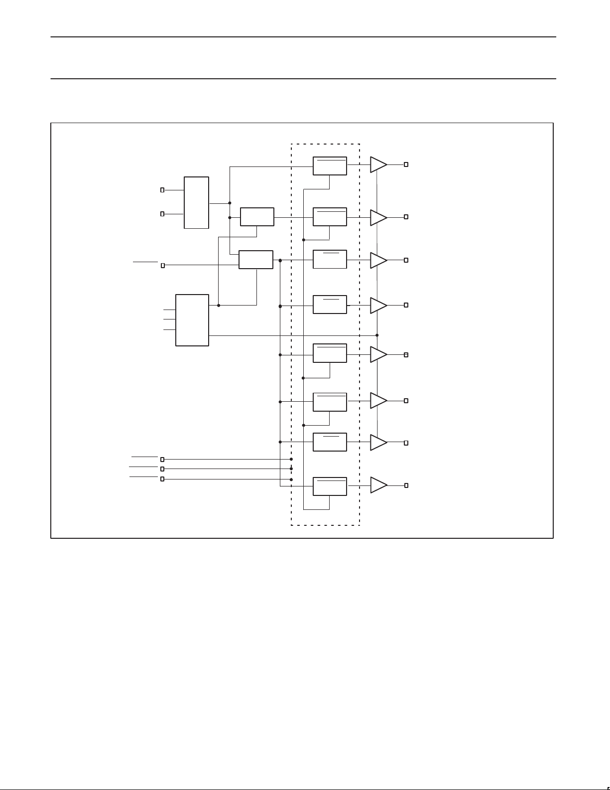
BLOCK DIAGRAM
XTAL_IN
X
14.318
MHZ
XTAL_OUT
SPREAD
SEL133/100
SEL0
SEL1
OSC
X
X
DECODE
LOGIC
USBPLL
SYSPLL
LOGIC
PWRDWN
LOGIC
PWRDWN
LOGIC
STOP
LOGIC
STOP
LOGIC
REF [0–1](14.318 MHz)
X
X
48 MHz USB
CPUCLK [0–3]
X
3V66 [0–3] (66MHz)
X
PCK2010R
PCISTOP
CPUSTOP
PWRDWN
PWRDWN
LOGIC
PWRDWN
LOGIC
STOP
LOGIC
X
X
X
PWRDWN
LOGIC
CPUDIV2 [0–1]
X
PCICLK_F (33MHz)
X
PCICLK [1–7] (33 MHz)
X
APIC [0–2] (16.67 MHz)
X
SW00505
2000 May 17
4
Philips Semiconductors Product specification
SIGNAL
SIGNAL STATE
CK98R (100/133MHz) RCC spread spectrum
PCK2010R
system clock generator
FUNCTION TABLE
SEL
133/100
NOTES:
1. Required for board level “bed-of-nails” testing.
2. Used to support Intel confidential application.
3. 48 MHz PLL disabled to reduce component jitter. 48 MHz outputs to be held Hi-Z instead of driven to LOW state.
4. “Normal” mode of operation.
5. TCLK is a test clock over driven on the XTALIN input during test mode. TCLK mode is based on 133 MHz CPU select logic.
6. Required for DC output impedance verification.
7. Frequency accuracy of 48 MHz must be +167 PPM to match USB default.
8. Range of reference frequency allowed is MIN = 14.316 MHz, NOMINAL = 14.31818 MHz, MAX = 14.32 MHz
SEL1 SEL0 CPU CPUDIV2 3V66 PCI 48 MHz REF IOAPIC NOTES
0 0 0 HI-Z HI-Z HI-Z HI-Z HI-Z HI-Z HI-Z 1
0 0 1 N/A N/A N/A N/A N/A N/A N/A 2
0 1 0 100 MHz 50 MHz 66 MHz 33 MHz HI-Z 14.318 MHz 16.67 MHz 3
0 1 1 100 MHz 50 MHz 66 MHz 33 MHz 48 MHz 14.318 MHz 16.67 MHz 4, 7, 8
1 0 0 TCLK/2 TCLK/4 TCLK/4 TCLK/8 TCLK/2 TCLK TCLK/16 5, 6
1 0 1 N/A N/A N/A N/A N/A N/A N/A 2
1 1 0 133 MHz 66 MHz 66 MHz 33 MHz HI-Z 14.318 MHz 16.67 MHz 3
1 1 1 133 MHz 66 MHz 66 MHz 33 MHz 48 MHz 14.318 MHz 16.67 MHz 4, 7, 8
CLOCK OUTPUT
USBCLK
7
TARGET FREQUENCY (MHz) ACTUAL FREQUENCY (MHz) PPM
48.0 48.008 167
CLOCK ENABLE CONFIGURATION
CPUSTOP PWRDWN PCISTOP CPUCLK CPUDIV2 APIC 3V66 PCI PCI_F REF / 48 MHz OSC VCOs
X 0 X LOW LOW LOW LOW LOW LOW LOW OFF OFF
0 1 0 LOW ON ON LOW LOW ON ON ON ON
0 1 1 LOW ON ON LOW ON ON ON ON ON
1 1 0 ON ON ON ON LOW ON ON ON ON
1 1 1 ON ON ON ON ON ON ON ON ON
NOTES:
1. LOW means outputs held static LOW as per latency requirement below
2. ON means active.
3. PWRDWN
4. All 3V66 clocks as well as CPU clocks should stop cleanly when CPUSTOP is pulled LOW.
5. CPUDIV2, IOAPIC, REF, 48 MHz signals are not controlled by the CPUSTOP functionality and are enabled all in all conditions except when
PWRDWN
pulled LOW, impacts all outputs including REF and 48 MHz outputs.
is LOW.
POWER MANAGEMENT REQUIREMENTS
LATENCY
NO. OF RISING EDGES OF FREE RUNNING PCICLK
CPUSTOP
PCISTOP
PWRDWN
NOTES:
1. Clock ON/OFF latency is defined as the number of rising edges of free running PCICLKs between the clock disable goes HIGH/LOW to the
first valid clock that comes out of the device.
2. Power up latency is when PWRDWN
goes inactive (HIGH) to when the first valid clocks are driven from the device.
0 (DISABLED) 1
1 (ENABLED) 1
0 (DISABLED) 1
1 (ENABLED) 1
1 (NORMAL OPERATION) 3 ms
0 (POWER DOWN) 2 MAX
2000 May 17
5
 Loading...