

Philips PCK2010DL Datasheet

INTEGRATED CIRCUITS
PCK2010
CK98 (100/133MHz) Spread Spectrum
System Clock Generator
Preliminary specification 1999 Mar 01
Philips Semiconductors Preliminary specification
CK98 (100/133MHz) Spread Spectrum System Clock
Generator
FEATURES
•Mixed 2.5V and 3.3V operation
•Four CPU clocks at 2.5V
•Eight PCI clocks at 3.3V, one free-running
(synchronous with CPU clocks)
•Four 3.3V fixed clocks @ 66MHz
•Two 2.5V CPUDIV2 clocks @ CPU clock frequency
•Three 2.5V IOAPIC clocks @ 16.67 MHz
•One 3.3V 48MHz USB clock
•Two 3.3V reference clocks @ 14.318 MHz
•Reference 14.31818 MHz Xtal oscillator input
•133 MHz or 100 MHz operation
•Power management control input pins
•LOW CPU clock jitter ≤ 250 ps cycle-cycle
•LOW skew outputs
•0.0ns – 1.5ns CPU - 3V66 delay
•1.5ns – 4.0ns 3V66 - PCI delay
•1.5ns – 4.0 ns CPU - IOAPIC delay
•Available in 56-pin SSOP package
•±0.5% center spread spectrum capability via select pins; –0.5%
down spread spectrum capability via select pins
DESCRIPTION
The PCK2010 is a clock synthesizer/driver chip for a PentiumII and
other similar processors.
The PCK2010 has four CPU clock outputs at 2.5V, two CPUDIV2
clock outputs running at CPU clock frequency (66MHz or 50MHz
depending on the state of SEL133/100) and four 3V66 clocks
running at 66MHz. There are eight PCI clock outputs running at
33MHz. One of the PCI clock outputs is free-running. Additionally,
the part has three 2.5V IOAPIC clock outputs at 16.67MHz and two
3.3V reference clock outputs at 14.318MHz. All clock outputs meet
Intel’s drive strength, rise/fall time, jitter , accuracy, and skew
requirements.
The part possesses dedicated power-down, CPUSTOP, and
PCISTOP input pins for power management control. These inputs
are synchronized on-chip and ensure glitch-free output transitions.
When the CPUSTOP input is asserted, the CPU clock outputs and
3V66 clock outputs are driven LOW. When the PCISTOP input is
asserted, the PCI clock outputs are driven LOW.
Finally, when the PWRDWN input pin is asserted, the internal
reference oscillator and PLLs are shut down, and all outputs are
driven LOW.
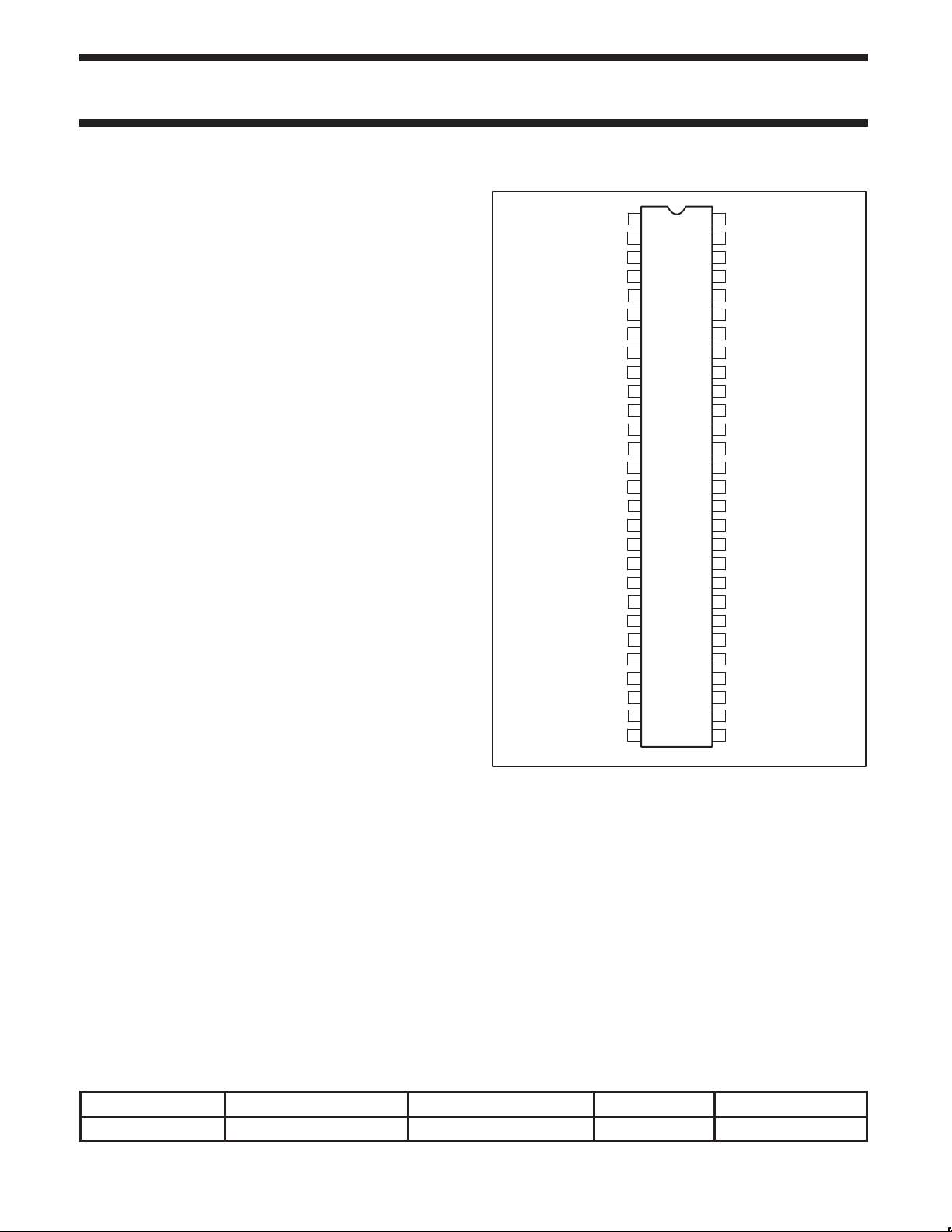
PIN CONFIGURATION
XTAL_IN
XTAL_OUT
PCICLK_F
PCICLK1
PCICLK2
PCICLK3
PCICLK4
PCICLK5
PCICLK6
PCICLK7
SEL133/100
V
REF0
REF1
VDD3V
V
VDD3V
V
VDD3V
V
V
3V66_0
3V66_1
VDD3V
V
3V66_2
3V66_3
VDD3V
PCK2010
1
SS
2
3
4
5
6
7
SS
8
9
10
11
12
13
SS
14
15
16
17
18
19
SS
20
SS
21
22
23
24
SS
25
26
27
28
56
55
54
53
52
51
50
49
48
47
46
45
44
43
42
41
40
39
38
37
36
35
34
33
32
31
30
29
VDD25V
APIC2
APIC1
APIC0
V
SS
VDD25V
CPUDIV2_1
CPUDIV2_0
V
SS
VDD25V
CPUCLK3
CPUCLK2
V
SS
VDD25V
CPUCLK1
CPUCLK0
V
SS
VDD3V
V
SS
PCISTOP
CPUSTOP
PWRDWN
SPREAD
SEL1
SEL0
VDD3V
48MHz
V
SS
SW00352
ORDERING INFORMA TION
PACKAGES TEMPERATURE RANGE OUTSIDE NORTH AMERICA NORTH AMERICA DRAWING NUMBER
56-Pin Plastic SSOP 0°C to +70°C PCK2010 DL PCK2010 DL SOT371-1
Intel and Pentium are registered trademarks of Intel Corporation.
1999 Mar 01
2

Philips Semiconductors Preliminary specification
CK98 (100/133MHz) Spread Spectrum System Clock
Generator
PIN DESCRIPTION
PIN NUMBER SYMBOL FUNCTION
2,3 REF [0–1] 3.3V 14.318 MHz clock output
5 XTAL_IN 14.318 MHz crystal input
6 XTAL_OUT 14.318 MHz crystal output
8 PCICLK_F 3.3V free running PCI clock
9, 11, 12, 14, 15, 17, 18 PCICLK [1–7] 3.3V PCI clock outputs
21, 22, 25, 26 3V66 [0–3] 3.3V fixed 66MHz clock outputs
28 SEL133/100
30 48MHz 3.3V fixed 48MHZ clock output
32, 33 SEL [0–1] Logic select pins. TTL levels.
34 SPREAD
35 PWRDWN
36 CPUSTOP
37 PCISTOP
41, 42, 45, 46 CPUCLK [0–3]
49, 50 CPUDIV_2 [0–1]
53, 54, 55 IOAPIC [0–2]
4, 10, 16, 23, 27, 31, 39 V
1, 7, 13, 19, 20, 24, 29, 38, 40, 44,
NOTES:
1. V
DD3V
on the performance of the device. In reality, the platform will be configured with the V
tied to a common 3.3V supply and all V
48, 52
43, 47, 51, 56 V
, V
and VSS in the above tables reflects a likely internal POWER and GROUND partition to reduce the effects of internal noise
DD25V
pins being common.
SS
DD3V
V
SS
DD25V
Select input pin for enabling 133MHz or 100MHz CPU outputs.
H = 133MHz, L = 100MHz
3.3V LVTTL input. Enables spread spectrum mode when held
LOW.
3.3V LVTTL input. Device enters powerdown mode when held
LOW.
3.3V LVTTL input. Stops all CPU clocks and 3V66 clocks when
held LOW. CPUDIV_2 output remains on all the time.
3.3V LVTTL input. Stops all PCI clocks except PCICLK_F when
held LOW.
2.5V CPU output. 133MHz or 100MHz depending on state of input
pin SEL133/100.
2.5V output running at 1/2 CPU clock frequency. 66MHz or 50MHz
depending on state of input pin SEL133/100.
2.5V clock outputs running divide synchronous with the CPU clock
frequency. Fixed 16.67 MHz limit.
3.3V power supply.
Ground
2.5V power supply
DD25V
PCK2010
pins tied to a 2.5V supply, all remaining V
DD
pins
1999 Mar 01
3

Philips Semiconductors Preliminary specification
CK98 (100/133MHz) Spread Spectrum System Clock
Generator
BLOCK DIAGRAM
LOGIC
PWRDWN
LOGIC
XTAL_IN
X
14.318
MHZ
XTAL_OUT
OSC
X
LOGIC
USBPLL
SYSPLL
PWRDWN
LOGIC
STOP
STOP
REF [0–1](14.318 MHz)
X
X
48MHz
CPUCLK [0–3]
X
3V66 [0–3] (66MHz)
X
PCK2010
SEL1
SPREAD
SEL133/100
PCISTOP
CPUSTOP
PWRDWN
PWRDWN
LOGIC
XSEL0
X
X
X
X
X
X
X
PWRDWN
LOGIC
STOP
PWRDWN
LOGIC
CPUDIV2 [0–1]
X
PCICLK_F (33MHz)
X
PCICLK [1–7] (33MHz)
X
APIC [0–2] ( PCI)
X
SW00353
1999 Mar 01
4
Philips Semiconductors Preliminary specification
CK98 (100/133MHz) Spread Spectrum System Clock
Generator
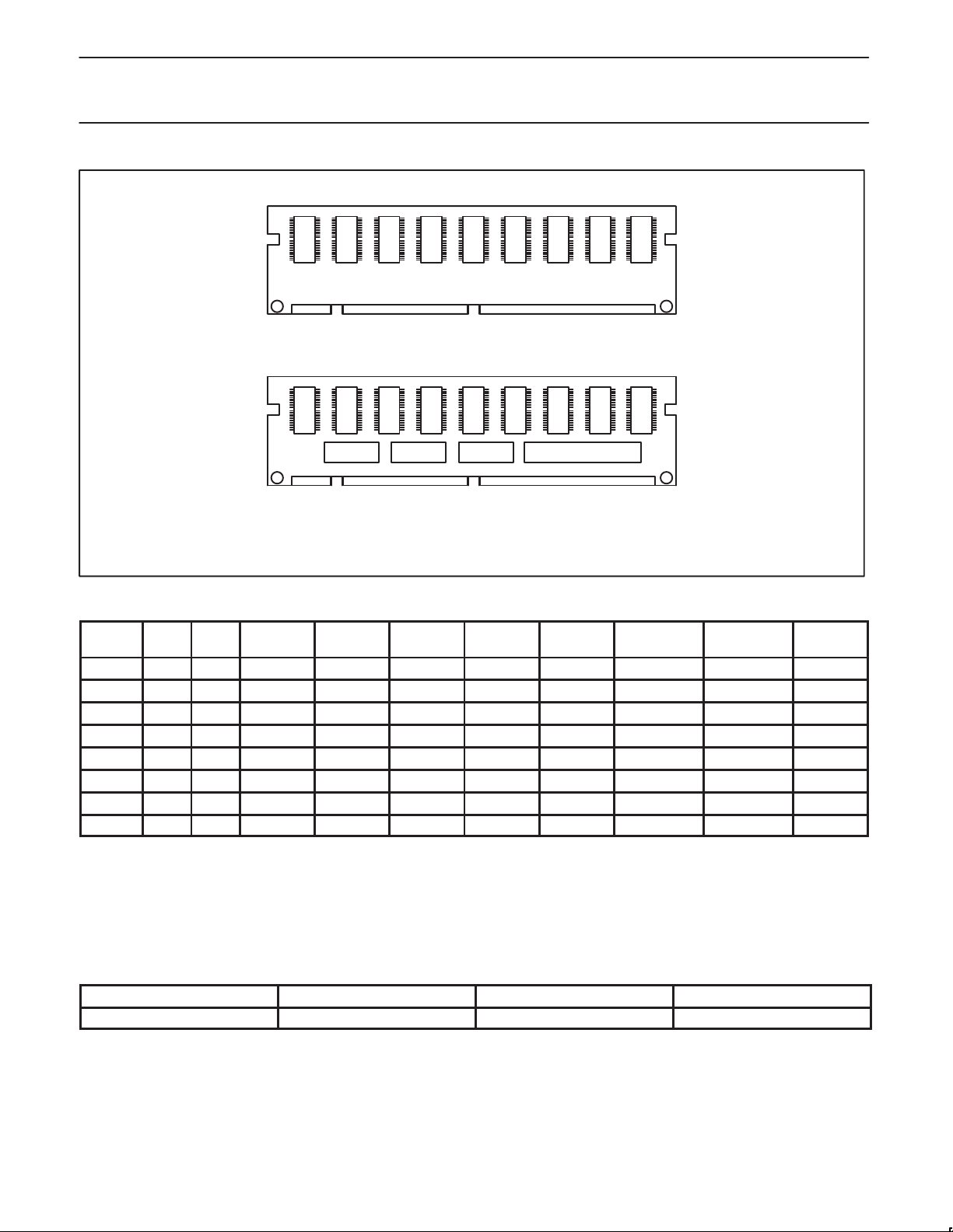
168-pin SDR SDRAM DIMM
SDRAM
SDRAM
SDRAM
SDRAM
SDRAM
SDRAM
SDRAM
SDRAM
SDRAM
BACK SIDE
FRONT SIDE
SDRAM
SDRAM
AVC
SDRAM
SDRAM
SDRAM
AVC PCK2509S or PCK2510SAVC
The PLL clock distribution device and SSTL registered drivers reduce
signal loads on the memory controller and prevent timing delays and
waveform distortions that would cause unreliable operation
SDRAM
SDRAM
PCK2010
SDRAM
SDRAM
SW00403
FUNCTION TABLE
SEL
133/100
NOTES:
1. Required for board level ‘‘bed-of-nails” testing.
2. Used to support Intel confidential application.
3. 48MHz PLL disabled to reduce component jitter. 48MHz outputs to be held Hi-Z instead of driven to LOW state.
4. ‘‘Normal” mode of operation.
5. TCLK is a test clock over driven on the XTALIN input during test mode. TCLK mode is based on 133MHz CPU select logic.
6. Required for DC output impedance verification.
7. Frequency accuracy of 48MHz must be +167 PPM to match USB default.
8. Range of reference frequency allowed is MIN = 14.316MHz, NOMINAL = 14.31818MHz, MAX = 14.32MHz
SEL1 SEL0 CPU CPUDIV2 3V66 PCI 48MHz REF IOAPIC NOTES
0 0 0 HI-Z HI-Z HI-Z HI-Z HI-Z HI-Z HI-Z 1
0 0 1 N/A N/A N/A N/A N/A N/A N/A 2
0 1 0 100MHz 50MHz 66MHz 33MHz HI-Z 14.318MHz 16.67MHz 3
0 1 1 100MHz 50MHz 66MHz 33MHz 48MHz 14.318MHz 16.67MHz 4, 7, 8
1 0 0 TCLK/2 TCLK/4 TCLK/4 TCLK/8 TCLK/2 TCLK TCLK/16 5, 6
1 0 1 N/A N/A N/A N/A N/A N/A N/A 2
1 1 0 133MHz 66MHz 66MHz 33MHz HI-Z 14.318MHz 16.67MHz 3
1 1 1 133MHz 66MHz 66MHz 33MHz 48MHz 14.318MHz 16.67MHz 4, 7, 8
CLOCK OUTPUT
USBCLK
7
TARGET FREQUENCY (MHz) ACTUAL FREQUENCY (MHz) PPM
48.0 48.008 167
1999 Mar 01
5
 Loading...