

Philips PCK2002PD, PCK2002PDP Datasheet
INTEGRATED CIRCUITS
PCK2002P
140 MHz PCI-X clock buffer
Product data
File under Integrated Circuits ICL03
2001 May 09
Philips Semiconductors Product data
PCK2002P140 MHz PCI-X clock buffer
FEA TURES
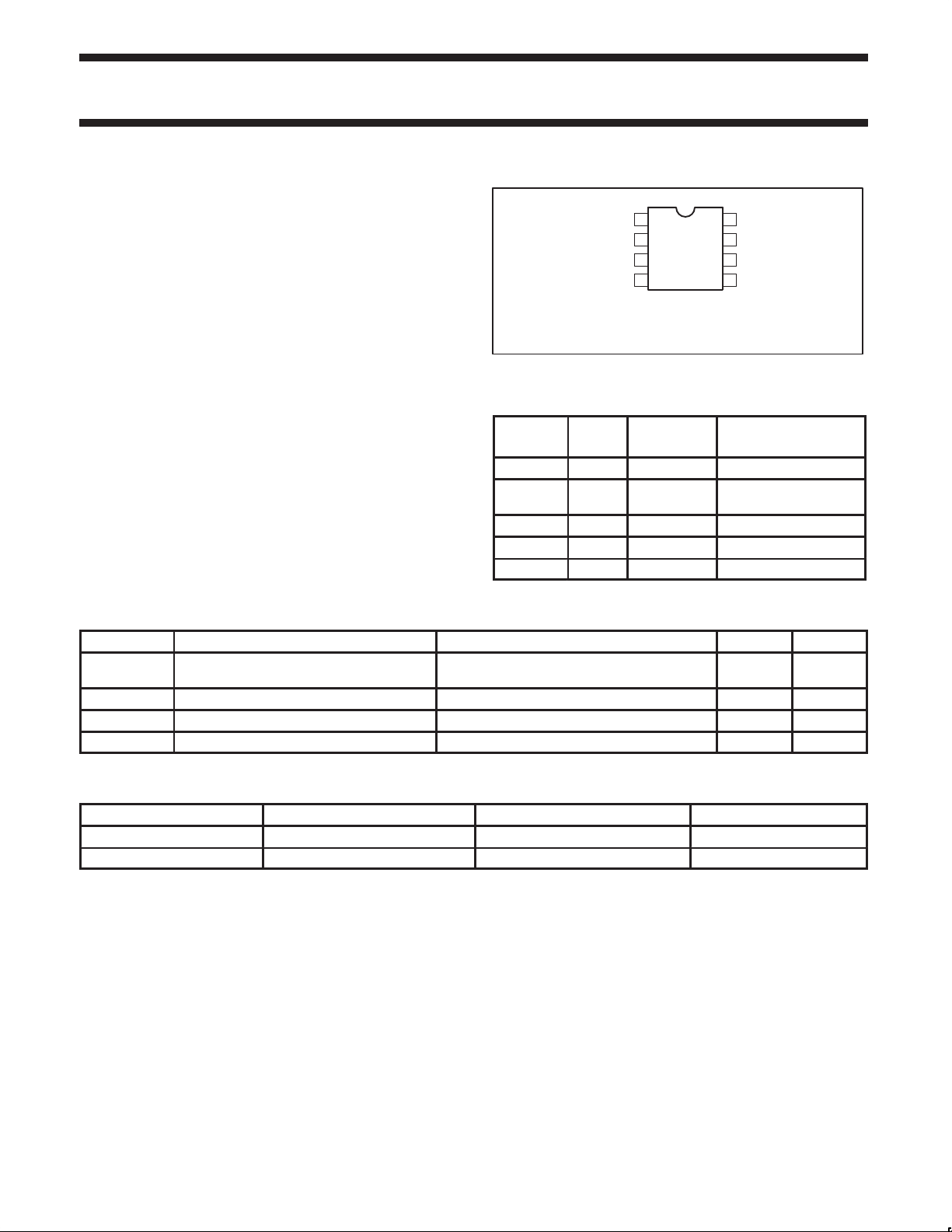
PIN CONFIGURATION
•General purpose and PCI-X 1:4 clock buffer
BUF_OUT3
•8-pin TSSOP package
•See PCK2001 for 48-pin 1:18 buffer part
•See PCK2001M for 28-pin 1:10 buffer part
BUF_IN
OE
BUF_OUT0
V
1
27
3
45
SS
8
6
PCK2002P
BUF_OUT2
V
DD
BUF_OUT1
•See PCK2001R for 16-pin 1:6 buffer part
•Operating frequency: 0 – 140 MHz
•Part-to-part skew < 500 ps
TOP VIEW
SA00552
•Low output skew: <200 ps
•3.3 V operation
•ESD classification testing is done to JEDEC Standard JESD22.
Protection exceeds 2000 V to HBM per method A114.
DESCRIPTION
The PCK2002PL is a 1–4 fanout buffer used as a high-performance,
low skew, general purpose and PCI-X clock buffer . It distributes one
input clock (BUF_IN) signal to four output clocks (BUF_OUT
QUICK REFERENCE DATA
SYMBOL PARAMETER CONDITIONS TYPICAL UNIT
t
t
I
PLH
PHL
t
t
CC
r
f
Propagation delay
BUF_IN to BUF_OUT
Rise time VCC = 3.3 V, CL = 25 pF, 0.2VDD to 0.6V
Fall time VCC = 3.3 V, CL = 25 pF, 0.6VDD to 0.2V
Total supply current VCC = 3.6 V 50 µA
n
).
n
VCC = 3.3 V, CL = 25 pF
PIN DESCRIPTION
PIN
NUMBER
1 Input BUF_IN Buffered clock input
3, 5, 7, 8 Output
6 Input V
2 Input OE Output Enable
4 Input V
I/O
TYPE
SYMBOL FUNCTION
BUF_OUT
(0–3)
DD
SS
DD
DD
Buffered clock outputs
3.3 V supply
Ground
2.9
2.8
800 ps
600 ps
ns
ORDERING INFORMATION
PACKAGES TEMPERATURE RANGE ORDER CODE DRAWING NUMBER
8-Pin Plastic TSSOP –40 to +85 °C PCK2002PDP SOT505-1
8-Pin Plastic SO –40 to +85 °C PCK2002PD SOT96-1
2001 May 09 853-2254 26252
2
Philips Semiconductors Product data
SYMBOL
PARAMETER
CONDITION
UNIT
SYMBOL
PARAMETER
CONDITIONS
UNIT
140 MHz PCI-X clock buffer
PCK2002P
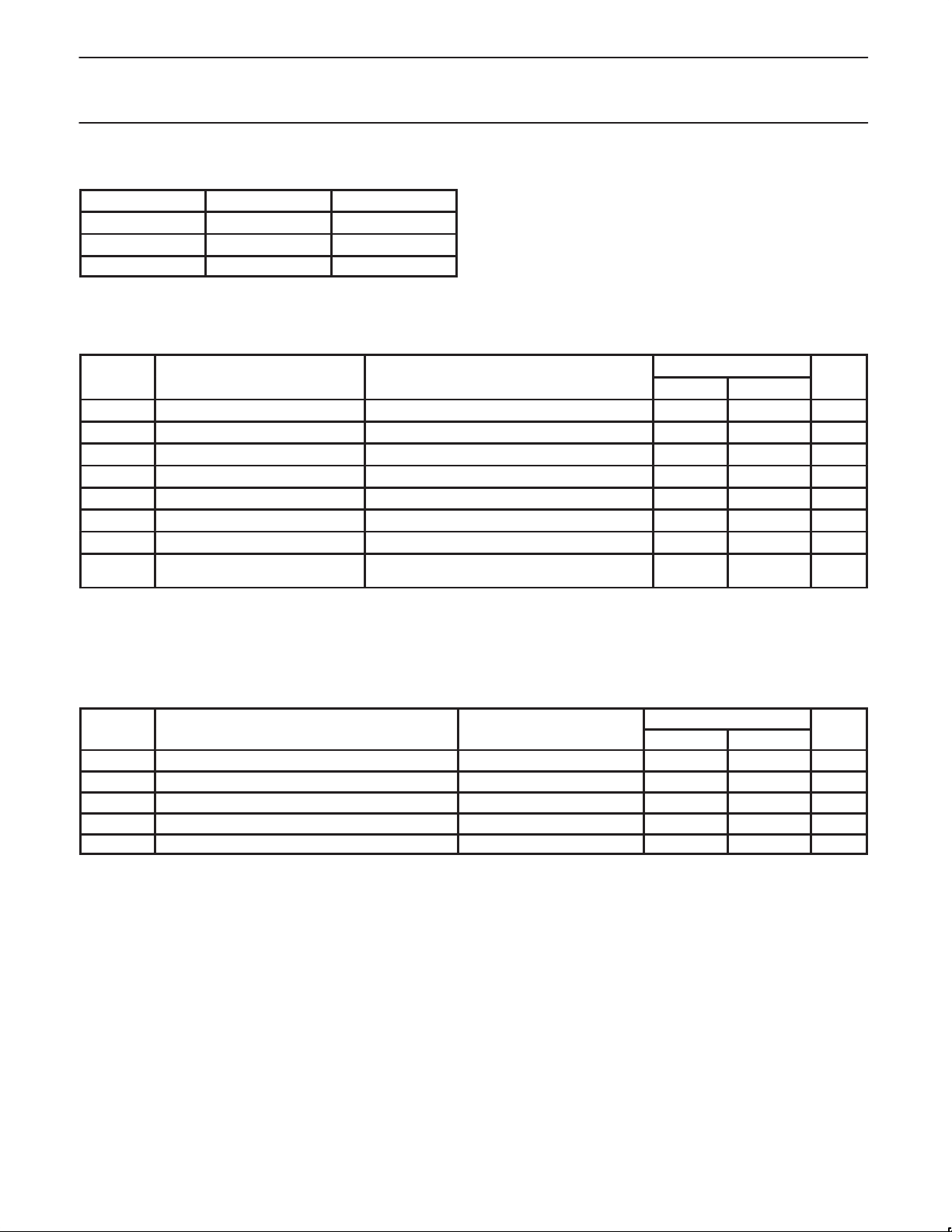
FUNCTION TABLE
OE BUF_IN BUF_OUTn
L X L
H L L
H H H
ABSOLUTE MAXIMUM RA TINGS
In accordance with the Absolute Maximum Rating System (IEC 134).
Voltages are referenced to V
V
DD
I
IK
V
I
OK
V
O
I
O
T
stg
P
tot
DC 3.3 V supply voltage –0.5 +4.3 V
DC input diode current VI < 0 — –50 mA
DC input voltage Note 2 –0.5 VDD + 0.5 V
I
DC output diode current VO > VDD or VO < 0 — ±50 mA
DC output voltage Note 2 –0.5 VDD + 0.5 V
DC output source or sink current VO ≥ 0 to V
Storage temperature range –65 +150 °C
Power dissipation per package
plastic medium-shrink SO (SSOP)
NOTES:
1. Stresses beyond those listed may cause permanent damage to the device. These are stress ratings only and functional operation of the
device at these or any other conditions beyond those indicated under “recommended operating conditions” is not implied. Exposure to
absolute-maximum-rated conditions for extended periods may affect device reliability .
2. The input and output voltage ratings may be exceeded if the input and output current ratings are observed.
(VSS = 0 V).
SS
1, 2
DD
For temperature range: 0 to +70 °C
above +55 °C derate linearly with 11.3 mW/K
LIMITS
MIN MAX
— ±50 mA
— 850 mW
RECOMMENDED OPERATING CONDITIONS
V
T
C
V
V
amb
DD
L
O
DC 3.3V supply voltage 3.0 3.6 V
Capacitive load 20 30 pF
DC input voltage range 0 V
I
DC output voltage range 0 V
Operating ambient temperature range in free air –40 +85 °C
LIMITS
MIN MAX
DD
DD
V
V
2001 May 09
3
 Loading...