

Philips PCK2002MDB, PCK2002MPW Datasheet

INTEGRATED CIRCUITS
PCK2002M
2
0–300 MHz I
Product data
File under Integrated Circuits ICL03
C 1:10 clock buffer
2001 Jul 19
Philips Semiconductors Product data
PCK2002M0–300 MHz I2C 1:10 clock buffer
FEA TURES
•HIGH speed, LOW noise non-inverting 1:10 buffer
•Mobile (reduced pincount) version of PCK2002
•Typically used to support two SDRAM DIMMs
•28-pin SSOP and TSSOP packages
•See PCK2002 for 48-pin 1-18 buffer part supporting up to
4 SDRAM DIMMs
•Optimized for 66 MHz, 100 MHz and 133 MHz operation
•Multiple V
and VSS pins for noise reduction
DD
DESCRIPTION
The PCK2002M is a 1–10 fanout buffer used for 133/100 MHz CPU,
66/33 MHz PCI, 14.318 MHz REF, or 133/100/66 MHz SDRAM
clock distribution. 10 outputs are typically used to support up to
2 SDRAM DIMMs commonly found in laptop or mobile applications.
The PCK2002M has the same features and operating characteristics
of the PCK2002 and is available in the SSOP 28 pin package.
All clock outputs meet Intel’s drive, rise/fall time, accuracy , and skew
requirements. An I
enabled/disabled individually. An output disabled via the I
interface will be held in the LOW state. In addition, there is an OE
input which 3-states all outputs.
2
C interface is included to allow each output to be
•Spread spectrum compliant
•175 ps skew outputs
•Individual clock output enable/disable via I
QUICK REFERENCE DATA
SYMBOL PARAMETER CONDITIONS TYPICAL UNIT
t
PLH
t
PHL
t
r
t
f
I
CC
ORDERING INFORMATION
28-Pin Plastic SSOP 0 to +70 °C PCK2002MDB SOT341–1
28-Pin Plastic TSSOP 0 to +70 °C PCK2002MPW SOT361–1
Propagation delay
BUF_IN to BUF_OUT
Rise time VCC = 3.3 V, CL = 30 pF 1.1 ns
Fall time VCC = 3.3 V, CL = 30 pF 1.0 ns
Total supply current VCC = 3.465 V 35 µA
PACKAGES TEMPERATURE RANGE ORDER CODE DRAWING NUMBER
2
C
n
VCC = 3.3 V, CL = 30 pF
2.7
2.9
2
C
ns
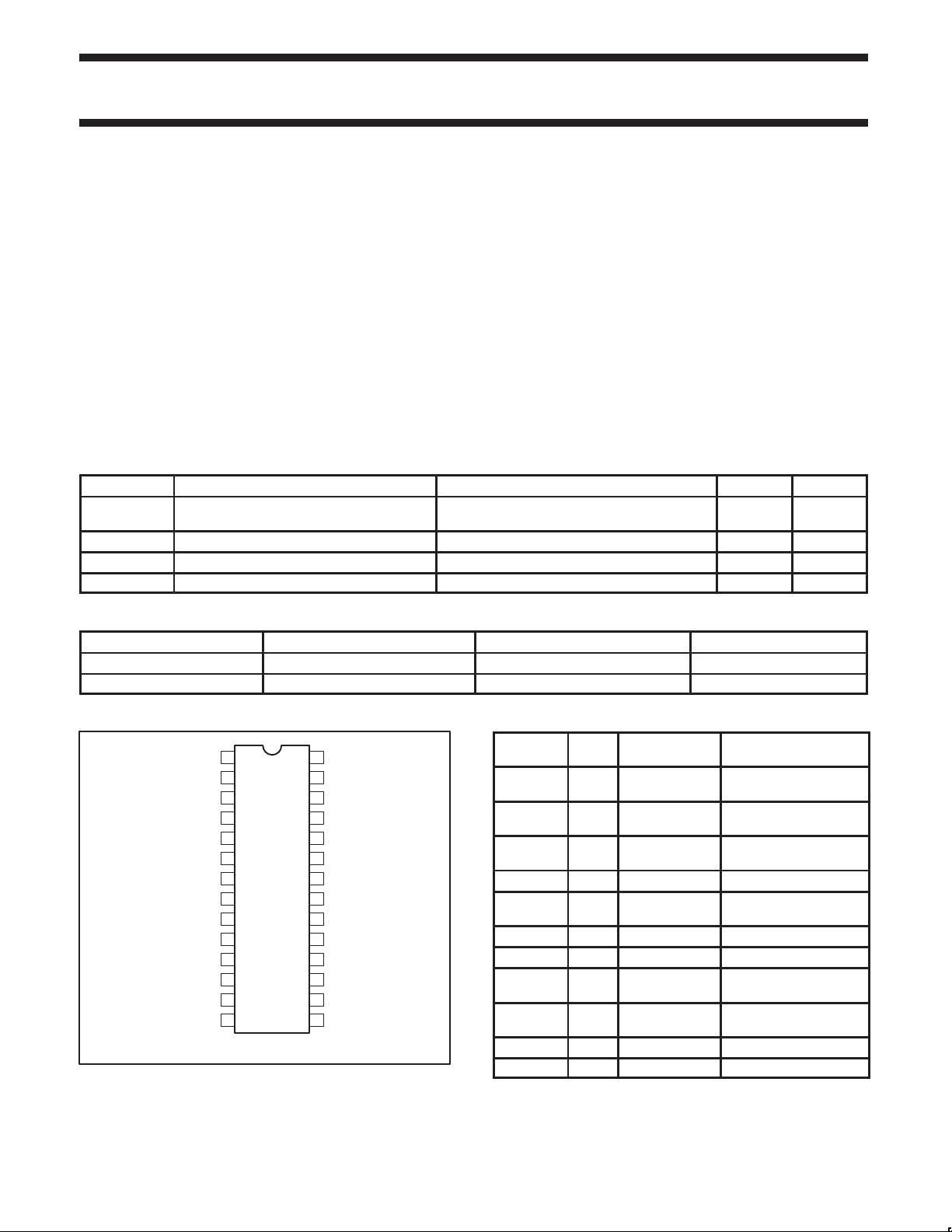
PIN CONFIGURATION
V
1
V
DD0
BUF_OUT0 BUF_OUT15
BUF_OUT1
BUF_OUT2
BUF_OUT3
BUF_OUT16 BUF_OUT17
Intel and Pentium are registered trademarks of Intel Corporation.
2
I
C is a trademark of Philips Semiconductors Corporation.
227
3
4
V
SS0
5
V
DD1
6
7
8
V
SS1
9
BUF_IN
10
V
DD4
11
12 17
V
SS4
13 16V
DDI2C
14 15SDA
TOP VIEW
28
DD9
BUF_OUT14
26
V
25
SS9
24
V
DD8
23
BUF_OUT13
22
BUF_OUT12
21
V
SS8
20
19
18
OE
V
DD5
V
SS5
V
SSI2C
SCL
SA00550
PCK2002M
PIN DESCRIPTION
PIN
NUMBER
2, 3, 6, 7 Output
22, 23, 26,
27
11, 18 Output
9 Input BUF_IN Buffered clock input
20 Input OE
14 I/O SDA I2C serial data
15 Input SCL I2C serial clock
1, 5, 10,
19, 24, 28
4, 8, 12,
17, 21, 25
13 Input V
16 Input V
I/O
TYPE
Output
Input V
Input V
SYMBOL FUNCTION
BUF_OUT
(0–3)
BUF_OUT
(12–15)
BUF_OUT
(16–17)
Buffered clock outputs
Buffered clock outputs
Buffered clock outputs
Active high output
enable
DD (0,1,4,5,8,9)
SS (0,1,4,5,8,9)
DDI2C
DDI2C
3.3 V power supply
Ground
3.3 V I2C power supply
I2C ground
2001 Jul 19 853-2268 26745
2
Philips Semiconductors Product data
SYMBOL
PARAMETER
CONDITION
UNIT
SYMBOL
PARAMETER
CONDITIONS
UNIT
2
0–300 MHz I
C 1:10 clock buffer
PCK2002M
FUNCTION TABLE
OE BUF_IN I2CEN BUF_OUTn
L X X Z
H L X L
H H H H
H H L L
ABSOLUTE MAXIMUM RA TINGS
In accordance with the Absolute Maximum Rating System (IEC 134)
Voltages are referenced to V
V
DD
I
IK
V
I
I
OK
V
O
I
O
T
stg
P
TOT
NOTES:
1. Stresses beyond those listed may cause permanent damage to the device. These are stress ratings only and functional operation of the
device at these or any other conditions beyond those indicated under “recommended operating conditions” is not implied. Exposure to
absolute-maximum-rated conditions for extended periods may affect device reliability .
2. The input and output voltage ratings may be exceeded if the input and output current ratings are observed.
DC 3.3 V supply voltage –0.5 +4.6 V
DC input diode current VI < 0 — –50 mA
DC output diode current VO > VDD or VO < 0 — ±50 mA
DC output source or sink current VO ≥ 0 to V
Storage temperature range –65 +150 °C
Power dissipation per package
plastic medium-shrink SO (SSOP)
(VSS = 0 V)
SS
DC input voltage Note 2 –0.5 4.6 V
DC output voltage Note 2 –0.5 VCC + 0.5 V
1, 2
DD
For temperature range: 0 to +70 °C
above +55 °C derate linearly with 11.3 mW/K
LIMITS
MIN MAX
— ±50 mA
— 850 mW
RECOMMENDED OPERATING CONDITIONS
LIMITS
MIN MAX
V
T
C
V
V
amb
DD
L
I
O
Operating ambient temperature range in free air 0 +70 °C
DC 3.3 V supply voltage 3.135 3.465 V
Capacitive load 20 30 pF
DC input voltage range 0 V
DC output voltage range 0 V
DD
DD
V
V
2001 Jul 19
3
Philips Semiconductors Product data
TEST CONDITIONS
VOH3.3 V output HIGH voltage
V
VOL3.3 V output LOW voltage
V
IOHOutput HIGH current
mA
IOLOutput LOW current
mA
2
0–300 MHz I
C 1:10 clock buffer
PCK2002M
DC CHARACTERISTICS
LIMITS
T
SYMBOL PARAMETER
V
IH
V
IL
HIGH level input voltage 3.135 to 3.465 2.0 VDD + 0.3 V
LOW level input voltage 3.135 to 3.465 VSS – 0.3 0.8 V
p
p
p
p
±I
I
±I
OZ
I
CC
∆I
CC
Input leakage current 3.465 — ±5 µA
3-State output OFF-State
current
Quiescent supply current 3.465 VI = VDD or GND IO = 0 — 100 µA
Additional quiescent supply
current given per control pin
VDD(V) OTHER MIN MAX
3.135 to 3.465 IOH = –1 mA VCC – 0.1 —
3.135 IOH = –36 mA 2.4 —
3.135 to 3.465 IOL= 1 mA — 0.1
3.135 IOL= 24 mA — 0.4
3.135 to 3.465 V
3.135 to 3.465 V
3.135 to 3.465 V
3.135 to 3.465 V
3.465 V
3.135 to 3.465 V
= 2.0 V –54 –126
OUT
= 3.135 V –21 –46
OUT
= 1.0 V 49 118
OUT
= 0.4 V 24 53
OUT
= VDD or GND IO = 0 — ±10 µA
OUT
= VDD– 0.6 V IO = 0 — 500 µA
I
= 0 to +70 °C UNIT
amb
2001 Jul 19
4
 Loading...