


查询PCF26100供应商查询PCF26100供应商
INTEGRATED CIRCUITS
DATA SH EET
PCF26100
Bluetooth Adapter IC
Preliminary specification
File under Integrated Circuits, IC17
2001 Jun 19

Philips Semiconductors Preliminary specification
Bluetooth Adapter IC PCF26100
CONTENTS
1 FEATURES
2 GENERAL DESCRIPTION
3 ORDERING INFORMATION
4 BLOCK DIAGRAM
5 PINNING INFORMATION
5.1 Pinning
5.2 Pin description
6 FUNCTIONAL DESCRIPTION
6.1 PCF26100 overview
6.2 BlueRF pin mapping
6.3 Timing
6.4 Serial interface
6.5 Registers
7 REFERENCE DOCUMENTS
8 LIMITING VALUES
9 DC CHARACTERISTICS
10 AC CHARACTERISTICS
11 APPLICATIONS
12 PACKAGE OUTLINE
13 SOLDERING
13.1 Introduction to soldering surface mount
packages
13.2 Reflow soldering
13.3 Wave soldering
13.4 Manual soldering
13.5 Suitability of surface mount IC packages for
wave and reflow soldering methods
14 DATA SHEET STATUS
15 DEFINITIONS
16 DISCLAIMERS
2001 Jun 19 2

Philips Semiconductors Preliminary specification
Bluetooth Adapter IC PCF26100
1 FEATURES
The PCF26100 performs the following functions:
• Power-on reset (reset)
• System clock generation for baseband controller
• Reference clock generation for the UAA3558
• Low-power clock generation for baseband controller
• Transmit clock generation for baseband controller
(1 MHz)
• Serial interface conversion between JTAG and 3-wire
S-bus
• Timing control generation for the UAA3558
• Transmit data conversion from digital-to-analog
gaussian shaped
• RSSI conversion from analog-to-digital and access
through serial JTAG interface
• Transmit PA control information from JTAG interface
digital-to-analog conversion
3 ORDERING INFORMATION
TYPE
NUMBER
PCF26100ET TFBGA48 plastic thin fine-pitch ball grid array package; 48 balls; 5 × 5 × 0.8 mm SOT641-1
NAME DESCRIPTION VERSION
• Provides radio ID through the serial JTAG interface
• System clock oscillator trimming.
2 GENERAL DESCRIPTION
The PCF26100is a mixed signal based adapter device for
wireless Bluetooth systems. The device adapts the
baseband interface of the Philips UAA3558 radio to the
Philips PCF26002 and PCF26003 baseband controller
devices and also to the BlueRF JTAG Unidirectional
RxMode 2.
The adapter is provided as a low risk solution to a working
Bluetooth system based on existing components. The
adapter ASIC implementation incorporates, as much as
possible, features to come to a complete Bluetooth
system, meeting the Bluetooth RF requirements.
From the Bluetooth system point of view the PCF26100 is
a transparent adaptation device between the baseband
controller and the UAA3558 radio.
PACKAGE
2001 Jun 19 3
Philips Semiconductors Preliminary specification
Bluetooth Adapter IC PCF26100
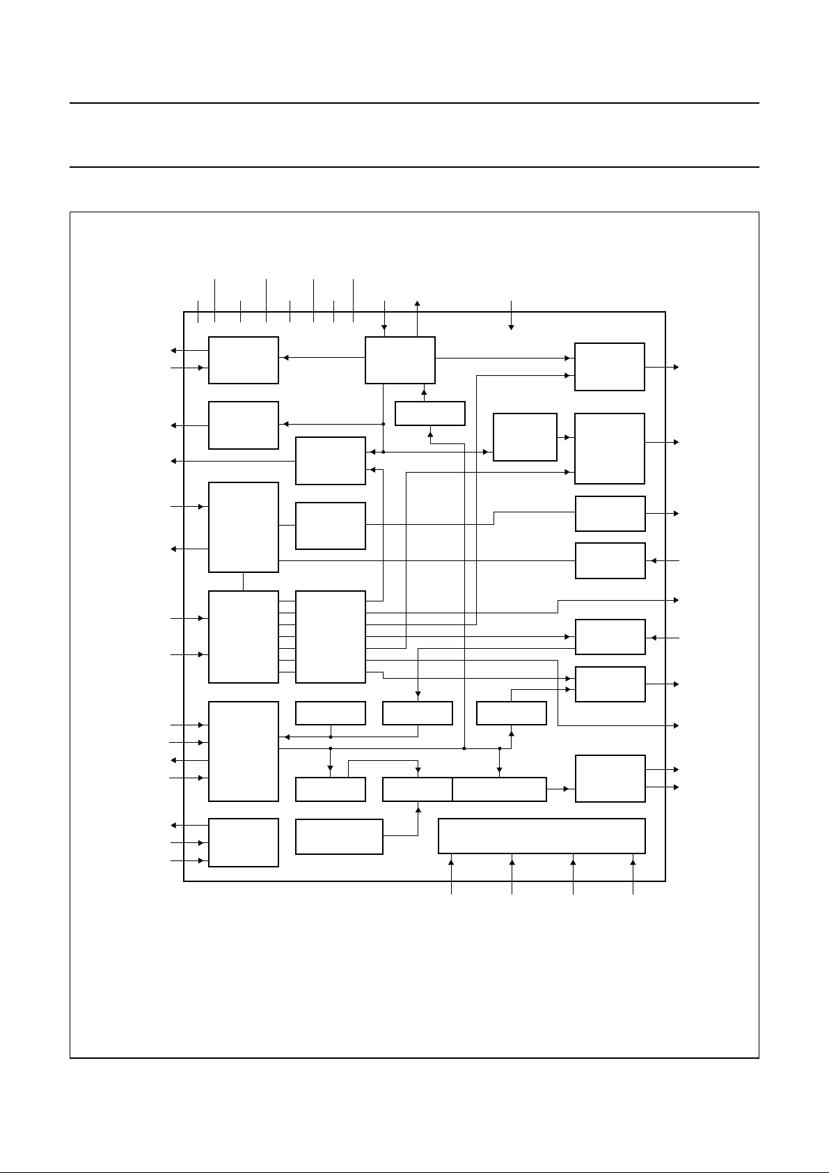
4 BLOCK DIAGRAM
handbook, full pagewidth
SYS_CLK
SYS_CLK_REQ
LPO_CLK
TX_CLK
TX_DATA
RX_DATA
SYNTH_ON
PX_ON
V
SS
V
DD
LOW POWER
V
SS(osc)
V
DD(osc)
SYSTEM
CLOCK
CLOCK
DIVIDER
RX/TX
MUX
TIMING
CONTROL
V
DD(I/O)
V
V
SS(I/O)
V
DDA
TRANSMIT
DATA CLOCK
DIVIDER
GFSK
FILTER
TIMING
SETTINGS
SSA
XIN
OSCILLATOR
MCLK
XOUT
XOTRIM
UBMODE
2.048 MHz
DIVIDER
PCF26100
REFERENCE
CLOCK
T_SW
MUX
DAC
RX SAMPLE
ADC
REF_CLK
T_SW
T_GFSK
R_DATA
SLCCTR
RSSI
SI_CMS
SI_CLK
SI_CDO
SI_CDI
POR
POR_EXT
VIO_POWER
SERIAL
INTERFACE
RESET
AND
POR
ID RSSI
CHANNEL
CHANNEL
CONVERSION
CHANNEL STATIC
Fig.1 Block diagram.
2001 Jun 19 4
DAC
PACNTL
3-WIRE
INTERFACE
TEST
SCANTEST TEST_EN ANATEST SHIFTCTRL
PACNTL
S_EN
S_DATA
S_CLK
MGT751
Philips Semiconductors Preliminary specification
Bluetooth Adapter IC PCF26100
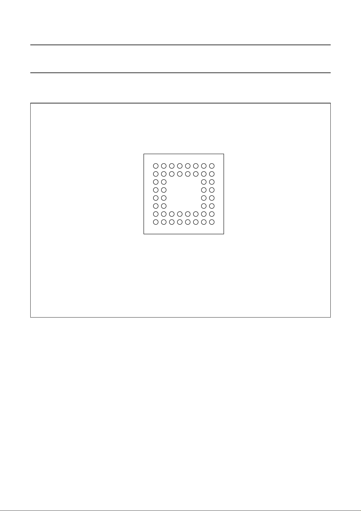
5 PINNING INFORMATION
5.1 Pinning
MBL245
H
G
F
E
D
C
B
A
PCF26100ET
246813
57
Fig.2 Pin configuration.
2001 Jun 19 5

Philips Semiconductors Preliminary specification
Bluetooth Adapter IC PCF26100
O3×CMOS output BB
controller
C1 core supply voltage P core power
E2 I/O ground supply P I/O ground
G2 core ground supply P core ground
H2 oscillator ground supply P oscillator ground
H5 oscillator supply voltage P oscillator power
G5 I/O supply voltage P I/O power
G7 I/O ground supply P I/O ground
E8, D8 analog ground supply P analog ground
This text is here in white to force landscape pages to be rotated correctly when browsing through the pdf in the Acrobat reader.This text is here in
_white to force landscape pages to be rotated correctly when browsing through the pdf in the Acrobat reader.This text is here inThis text is here in
white to force landscape pages to be rotated correctly when browsing through the pdf in the Acrobat reader. white to force landscape pages to be ...
5.2 Pin description
Table 1 Pin description for the TFABGA48 package
2001 Jun 19 6
SYMBOL BALL DESCRIPTION I/O SIGNAL TYPE SOURCE
POR A1 reset output to baseband controller O 1 × CMOS output BB
SHIFTCTRL C2 test mode I non-inverting CMOS input with pull-down test
DD
LPO_CLK D1 3.2 kHz low-power clock to baseband controller O 1 × CMOS output BB
VIO_POWER B1 power-on reset reference I Schmitt-trigger input
V
PX_ON E1 receive packet synchronization correlation achieved I non-inverting CMOS input BB
SS(I/O)
V
SYS_CLK_REQ F1 system clock control input from baseband controller I non-inverting CMOS input BB
SYS_CLK G1 controlled system clock output to baseband
TX_CLK F2 transmit data clock output to baseband controller O 1 × CMOS output BB
SS
RX_DATA H1 receive data output to baseband controller O 1 × CMOS output BB
V
ANATEST G3 test mode I non-inverting CMOS input with pull-down test
SS(osc)
XOUT H3 oscillator output O oscillator output misc
V
XIN H4 oscillator input I oscillator input misc
DD(osc)
V
V
DD(I/O)
POR_EXT H6 reset and POR on control input I non-inverting CMOS input host
TEST_EN H7 test mode I non-inverting CMOS input with pull-down test
SS(I/O)
SLCCTR G6 DC offset control to UAA3558 O 1 × CMOS output
V
S_EN H8 serial interface and timing control output to UAA3558 O 1 × CMOS output UAA
S_CLK F7 serial interface clock output to UAA3558 O 1 × CMOS output UAA
S_DATA G8 serial interface data output to UAA3558 O 1 × CMOS output UAA
SSA
REF_CLK F8 reference clock output to UAA3558 O 3 × CMOS output UAA
V
RSSI D7 RSSI analog input from UAA3558 I analog input UAA
T_GFSK C8 analog transmit data output to UAA3558 O analog output UAA

Philips Semiconductors Preliminary specification
Bluetooth Adapter IC PCF26100
I non-inverting CMOS input UAA
O3×CMOS output UAA
output = 0 to 2.2 V)
multiplexed with 2.048MHz clock output
C7 analog supply voltage P analog power
A6 I/O ground supply P I/O ground
B4 I/O supply voltage P I/O power
I non-inverting CMOS input BB
controller
SYMBOL BALL DESCRIPTION I/O SIGNAL TYPE SOURCE
This text is here in white to force landscape pages to be rotated correctly when browsing through the pdf in the Acrobat reader.This text is here in
_white to force landscape pages to be rotated correctly when browsing through the pdf in the Acrobat reader.This text is here inThis text is here in
white to force landscape pages to be rotated correctly when browsing through the pdf in the Acrobat reader. white to force landscape pages to be ...
PACNTL B8 analog PA control output to external PA O analog output misc
2001 Jun 19 7
DDA
V
R_DATA B7 receive data input from UAA3558 (UAA3558
T_SW A8 transmit switch timing control to UAA3558
SCANTEST B6 test mode I non-inverting CMOS input with pull-down test
TX_DATA A7 transmit data I non-inverting CMOS input BB
SS(I/O)
V
SYNTH_ON A5 timing control input from baseband controller I non-inverting CMOS input BB
UBMODE A4 unidirectional/bidirectional mode selection I non-inverting CMOS input misc
DD(I/O)
V
SI_CLK A3 serial interface clock input from baseband controller I non-inverting CMOS input BB
SI_CMS A2 serial interface mode select input from baseband
SI_CDI B3 serial interface data input from baseband controller I non-inverting CMOS input BB
SI_CDO B2 serial interface data output to baseband controller O 1 × CMOS output BB

Philips Semiconductors Preliminary specification
Bluetooth Adapter IC PCF26100
6 FUNCTIONAL DESCRIPTION
6.1 PCF26100 overview
The adapter features a Power-on reset which is used to
reset the adapter logic. There is also a POR_EXT signal
which is used for controlling the reset of the PCF26100
within the application.
The system clock for the application is generated by the
PCF26100. The system clock is then provided to the
baseband SYS_CLK and the radio REF_CLK. Both the
SYS_CLK and REF_CLK clocks are controlled within the
PCF26100.
From the system clock a low-power 3.2 kHz clock
LPO_CLK is generated.
From the PCF26100 a 1 MHz TX_CLK is generated to be
used in the baseband controller to clock out the transmit
data on TX_DATA.
The serial interface to the baseband controller is a JTAG
interface. This interface is used toinitialize and control the
PCF26100 and subsequently the radio. The channel
information received from theJTAG interface is converted
and forwarded to the radio 3-wire S-bus interface.
The timing control signals to the UAA3558 radio are
generated in the PCF26100. For this a minimum number
of reference timing signals from the baseband controller
are used. The exact timing of the control signals is
programmable in the PCF26100.
The PCF26100 converts the digital transmit data from the
baseband controller to analog gaussian shaped transmit
data to the radio.
The analog RSSI from the radio is converted to digital and
made available to the baseband controller via the JTAG
interface.
The digital power amplifier control information
communicated from the baseband controller to the
PCF26100isconvertedto an analog control voltageforthe
radio.
The PCF26100 provides an identification number, which
can be read by the baseband controller through the JTAG
interface.
For frequency compensation and tuning, the PCF26100
provides a tuning capability on the system oscillator.
6.2 BlueRF pin mapping
Table 2 Adapter and BlueRF unidirectional pin mapping.
ADAPTER TO
BASEBAND PIN NAME
POR_EXT BnPWR
POR not applicable
LPO_CLK not applicable
SYS_CLK not applicable
SYS_CLK_REQ BXTLEN
TX_CLK BRCLK
TX_DATA BTXD/BDATA1
RX_DATA BRXD
SYNTH_ON BSEN
PX_ON BPKTCTL/BDATA2
SI_CMS BnDEN
SI_CLK BDCLK
SI_CDI BMOSI/BDDATA
SI_CDO BMISO
VIO_POWER not applicable
BLUERF PIN NAME JTAG
UNIDIRECTIONAL
RXMODE 2
2001 Jun 19 8
Philips Semiconductors Preliminary specification
Bluetooth Adapter IC PCF26100
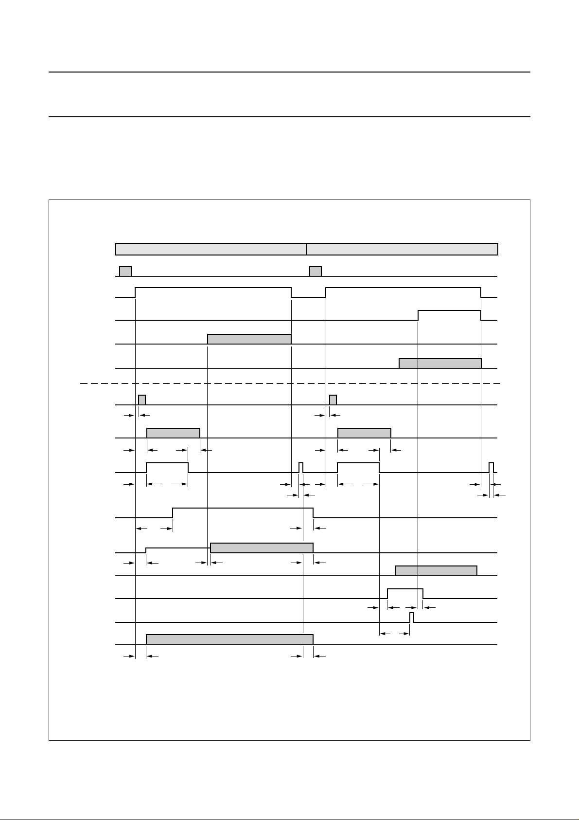
6.3 Timing
The timing for the radio is generated in the PCF26100 using a minimal number of baseband signals. The channel
programming is received from the JTAG serial interface. The SYNTH_ON signal is used to determine the start and end
of the packet. The radio SLCCTR signals is also controlled with PX_ON.
handbook, full pagewidth
JTAG
SYNTH_ON
PX_ON
TX_DATA
RX_DATA
S_xxx
REF_CLK
S_EN
T_SW
RX packetTX packet
t
1
t
2
t
5
t
17
t
3
t
6
t
7
t
9
t
1
t
2
t
5
t
18
t
3
t
6
t
8
t
9
T_GFSK
R_DATA
SLCCTR
RSSI
TX_CLK
t
10
t
10
t
11
Fig.3 Detailed timing diagram.
2001 Jun 19 9
t
12
t
13
t
4
t
12
t
14
MGT756

Philips Semiconductors Preliminary specification
Bluetooth Adapter IC PCF26100
Table 3 Adapter timing parameters
PARAMETER DESCRIPTION VALUE UNIT
t
1
t
2
t
3
t
4
t
5
t
6
t
7
t
8
t
9
t
10
t
11
t
12
t
13
t
14
t
17
t
18
SYNTH_ON rising edge to 3-wire serial data 0.35 µs
SYNTH_ON rising edge to REFCLK start S_EN start µs
S_EN falling edge to REFCLK stop delay 2 µs
S_EN falling edge to RSSI measurement RSSI_start µs
SYNTH_ON rising edge to S_EN rising edge S_EN start µs
S_EN width S_EN width µs
SYNTH_ON falling edge to S_EN pulse rising edge S_EN pulse start µs
SYNTH_ON falling edge to S_EN pulse rising edge S_EN pulse start µs
S_EN pulse width 2 µs
SYNTH_ON rising edge to T_GFSK DC bias and TXCLK
GFSK_DC_bias start µs
enable
TX_DATA digital in to T_GFSK analog out delay 14 13 MHz cycles
S_EN pulse falling edge to T_GFSK LOW and TXCLK
0 µs
disable
S_EN falling edge to SLCCTR rising edge SLCCTR start µs
PX_ON rising edge to SLCCTR falling edge 0 µs
SYNTH_ON rising edge to T_SW rising edge T_SW start µs
S_EN pulse falling edge to T_SW falling edge 0 µs
6.3.1 T_GFSK
The T_GFSK data output has 3 phases:
1. Idle phase
2. DCbias phase
3. Txdata phase.
The Idle phase is used outside transmit packets. In this
phase the T_GFSK output state is defined by the
‘gfsk float’ bit in the Enable Register.If the ‘gfsk float’ bit is
set to a logic 0, the T_GFSK output is pulled to ground; if
set to a logic 1 the T_GFSK output is floating.
The DCbias phase is used during the transmit slot as
start-up phase before the transmit data. The DCbias
phase is activeGFSK_DC_BIAS_Start delayfollowing the
S_EN rising edge until the first transmit data bit on
TX_DATA.
During this phase a DC bias is generated by the GFSK
filter, which is achieved by selecting the GFSK table
mid-value as the output of the GFSK filter.
The Txdata phase is used when TXDATA is present.
In this phase the TX_DATA is fed into the GFSK filter. The
presence of TXDATA is determined by detecting the first
TXDATA edge. The end of the TXDATA is detected by the
end of packet from the baseband controller. To not lose
TXDATA information in the T_GFSK output, due to the
data detection, the data from the GFSK input is delayed
with 1-bit.
The T_GFSK output requires an external low-pass filter.
Thereference voltage for theT_GFSKcomes directly from
the V
relation to a variation in the T_GFSK levels. The V
power supply. Any variation on V
DDA
has a direct
DDA
DDA
power supply shouldbe provided froma voltage reference.
The TX_CLK output is activated during the DC_BIAS
phase and the Txdata phase.
2001 Jun 19 10

Philips Semiconductors Preliminary specification
Bluetooth Adapter IC PCF26100
6.3.2 RESET
The PCF26100 is reset with a Power-on reset using the
VIO_POWER signal. This will reset all registers and put
the device into a known state. The POR_EXT reset signal
will also resetthe device andput it inthe same state as the
Power-on reset. However, POR_EXT is intended to be
used for a reset from a host.
Following the Power-on reset or areset by POR_EXT, the
system oscillator is started and the SYS_CLK output is
activated (enabled). The SYS_CLK output can be
controlledbythe SYS_CLK_REQ signal butonlyifthe ‘rdy’
bit in the Control Register has been set to logic 1.
handbook, full pagewidth
VIO_POWER
OSC
SYS_CLK_REQ
The function of SYS_CLK_REQ has 2 phases:
1. After reset, SYS_CLK_REQ is not taken into account
forthegenerationof SYS_CLK. After reset the13 MHz
system clock is enabled on SYS_CLK.
2. Once the ‘rdy’ bit is set to logic 1, the 13 MHz clock on
the SYS_CLK is controlled with SYS_CLK_REQ.
The SYS_CLK_REQ signal will not control or disable the
oscillator.
The LPO_CLK output is only controlled by the POR_EXT
signal which also controls the POR output. The POR is
activated 4 SYS_CLK cycles after POR_EXT.
SYS_CLK
POR_EXT
POR
LPO_CLK
phase 1 Rdy = 0 phase 2 Rdy = 1
MGT755
Fig.4 Reset timing.
2001 Jun 19 11

Philips Semiconductors Preliminary specification
Bluetooth Adapter IC PCF26100
6.4 Serial interface
6.4.1 3-WIRE S-BUS
The 3-wire S-bus at the radio side is a 32-bit serial interface which is used for control, TX/RX and channel information.
The 32-bit definition is given in Tables 4 and 5.
Bits 31 to 9 arestatic values and will not change dynamically,the value for these bitscome fromthe static registers. Only
thetrx and main dividerfields will control theUAA3558on a slot-by-slotbasis.The trx andmaindivider information comes
fromthe baseband controllerserial interface channelword;see Section 6.5.1. However,the baseband controllerchannel
information needs a conversion to get the correct main divider information for the UAA3558.
Table 4 UAA3558 3-wire programming word
31 30 29 28 27 26 25 24 23 22 21 20 19 18 17 16
test dpo BW adjust strc sdsn sdco ssqs ssth dmo tin
Table 5 UAA3558 3-wire programming word (continued)
1514131211109876543210
tsw tamp ref1 ref0 txp1 txp0 pll trx main divider (n)
6.4.2 JTAG
The JTAG serial interface is usedto control the PCF26100 and subsequently the radio. ThePCF26100 must be the only
slave on the JTAG bus as the PCF26100 does not allow for multi-slave operation. The JTAG interface protocol used is
fully compliant with the standard set out in
• 5-bit register address
• 8-bit data
• Set instruction register
• Read/write data register (note: some addresses have a separate read and write data register).
TheJTAG interface allowsfor 2 ways ofaccessing a register.One is thecommunicate address anddata, and thesecond
one is for successive accesses to the same registers where only the data is communicated. This can, for example, be
used for updating the channel information before every packet.
“IEEE Std 1149.1-1990”
. The following features are supported:
2001 Jun 19 12

Philips Semiconductors Preliminary specification
Bluetooth Adapter IC PCF26100
6.5 Registers
The registers that are controlled via the serial interface are shown in Table 6.
Table 6 Register map
REGISTER TYPE
S_EN_start R/W 8 0C S_EN start delay
S_EN_width R/W 9 C8 S_EN width
T_SW_start R/W 10 64 T_SW start delay
SLCCTR_start R/W 11 0A SLCCTR start delay
S_EN_PULSE_start R/W 12 02 S_EN pulse start delay
RSSI_start R/W 13 64 RSSI measurement position
STATIC_B15_9 R/W 14 24 UAA3558 serial word static values
STATIC_B23_16 R/W 15 12 UAA3558 serial word static values
STATIC_B31_24 R/W 16 00 UAA3558 serial word static values
CHANNEL W 18 00 frequency channel number and TX/RX information
RSSI R 18 00 RSSI
XO-trim W 19 80 trim value for the system clock oscillator
ID R 19 A1 device identification
CONTROL R/W 22 00 system clock control
PACONTROL R/W 24 00 for external PA power control
ENABLE R/W 25 00 adapter control
GFSK_DC_BIAS_start R/W 26 64 GFSK DC bias start delay
GFSK_TABLE R/W 28 00 GFSK look-up table values
RXFREQ W 30 61 RX channel conversion number
TXFREQ W 31 60 TX channel conversion number
ADDRESS
(DECIMAL)
RESET
(HEX)
DESCRIPTION
6.5.1 CHANNEL PROGRAMMING
The serial interface channel programming word is forwarded to the UAA3558 3-wire interface. The channel information
cannot normally be used directly and needs a conversion to get the right number for the UAA3558.
Table 7 Channel programming word
ADDRESS 76543210
18 (decimal) trx channel number (m)
Table 8 Description of Channel programming word bits
BIT DESCRIPTION
7 If trx = 0, then device in Transmit mode. If trx = 1, then device in Receive mode.
6 to 0 These 7 bits determine the channel number (m).
2001 Jun 19 13

Philips Semiconductors Preliminary specification
Bluetooth Adapter IC PCF26100
6.5.2 FREQUENCY CHANNEL CONVERSION
The conversion number is programmable for TX and RX. The function implemented is:
TX frequency = 2304+m+TXFREQ; where m is the BT channel number and TXFREQ is programmable between
0 and 255
RX frequency = 2304+m+RXFREQ; where m is the BT channel number and RXFREQ is programmable between
0 and 255.
Table 9 Frequency conversion word RXFREQ
ADDRESS 76543210
30 (decimal) RXFREQ
Table 10 Frequency conversion word TXFREQ
ADDRESS 76543210
31 (decimal) TXFREQ
6.5.3 STATIC VALUES
The UAA3558 bits 31 to 9 are static values and will not change dynamically. These values are programmed into the
adapter via the serial interface. The static words are: STATIC_B15_9, STATIC_B23_16 and STATIC_B31_24.
Table 11 Static word STATIC_B15_9
ADDRESS 76543210
14 (decimal) static value bits 15 to 9 not used
Table 12 Static word STATIC_B23_16
ADDRESS 76543210
15 (decimal) static value bits 23 to 16
Table 13 Static word STATIC_B31_24
ADDRESS 76543210
16 (decimal) static value bits 31 to 24
2001 Jun 19 14

Philips Semiconductors Preliminary specification
Bluetooth Adapter IC PCF26100
6.5.4 TIMING VALUES
The UAA3558 needs some timing signals which do not have a corresponding signal at the BlueRF interface. These
signals are generated internally in the adapter. The timing values for these will not change dynamically. These values
are programmed into the adapter via the serial interface. The timing words are: S_EN_start, S_EN_width, T_SW_start,
SLCCTR_start, S_EN_PULSE_start, RSSI_start, and GFSK_DC_bias.
Table 14 Timing control word S_EN_start
ADDRESS 76543210
8 (decimal) programmed timing value (resolution of 1-bit = 1 µs)
Table 15 Timing control word S_EN_width
ADDRESS 76543210
9 (decimal) programmed timing value (resolution of 1-bit = 1 µs)
Table 16 Timing control word T_SW_start
ADDRESS 76543210
10 (decimal) programmed timing value (resolution of 1-bit = 1 µs)
Table 17 Timing control word SLCCTR_start
ADDRESS 76543210
11 (decimal) programmed timing value (resolution of 1-bit = 1 µs)
Table 18 Timing control word S_EN_PULSE_start
ADDRESS 76543210
12 (decimal) programmed timing value (resolution of 1-bit = 1 µs)
Table 19 Timing control word RSSI_start
ADDRESS 76543210
13 (decimal) programmed timing value (resolution of 1-bit = 1 µs)
Table 20 Timing control word GFSK_DC_bias
ADDRESS 76543210
26 (decimal) programmed timing value (resolution of 1-bit = 1 µs)
2001 Jun 19 15

Philips Semiconductors Preliminary specification
Bluetooth Adapter IC PCF26100
Table 21 Register values range and actual timings
REGISTER RANGE TIMING ACTUAL VALUE UNIT
S_EN_START 0 < x < 256 t2and t5S_EN_START + (0 to 1) µs
S_EN_WIDTH 0 < x < 256 t
T_SW_START S_EN_START < x < 256 t
SLCCTR_START 0 < x < 256 t
S_EN_PULSE_DEL 0 < x < 256 t
RSSI_START 0< x < 256 t
GFSK_DC_BIAS 0 < x < 256 t
6
17
13
and t8S_EN_PULSE_DEL + (0 to 1) µs
7
4
10
6.5.5 RSSI
The RSSI is read via the serialinterface. TheUAA3558 providesan analog RSSI output. The interface logic converts the
analog RSSI value and stores the result in a serial interface register. The timing for converting the RSSI is programmed
using the RSSI_start register. The RSSI can only be measured starting 10 µs after the S_EN falling edge. The RSSI
value can only be read from the serial interface register after the measurement has been completed, this is at the end of
the packet. RSSI measurements are only done in receive packets.
S_EN_WIDTH µs
T_SW_START + (0 to 1) µs
SLCCTR_START + 1 µs
RSSI_START µs
GFSK_DC_BIAS + (0 to 1) µs
Table 22 RSSI control word
ADDRESS 76543210
18 (decimal) RSSI
6.5.6 T
RANSMIT POWER CONTROL
The transmit power can be controlled from a serial interface register. The 8-bit transmit power control word is used to
control the PA DAC. Writing to the PA DAC register will directly change the PA DAC output. The PA control register
should be written when the transmitter is not active.
Table 23 Unidirectional JTAG PA control word
ADDRESS 76543210
24 (decimal) PA power control
6.5.7 GFSK
TABLE
The values for the GFSK filter are stored in a 13-byte GFSK table. The GFSK table is accessed through a single control
word which is used to store the data in the GFSK table on subsequent writes. To align the writing to the GFSK table a
table address reset bit is available in the Enable register. When the resetbit ‘grst’ in the Enable register is set toa logic 1
the GFSK table address will be reset and the next GFSK control word is written at location 0 in the GFSK table. Every
subsequent write to the GFSK control word will be stored at the next address in the GFSK table. If the last address is
reached, subsequent writes will continue to effect the last address.
The values for the GFSK table depend on the reference voltage on V
. The T_GFSK signal should have a DC_Bias
DDA
of 1.2 V with a peak-to-peak swing of 1 V (amplitude = 0.5 V). For this the values for the GFSK table are calculated as
shown in Table 26.
Table 24 Unidirectional JTAG GFSK control word
GFSK_TABLE 76543210
28 (decimal) GFSK table value
2001 Jun 19 16

Philips Semiconductors Preliminary specification
Bluetooth Adapter IC PCF26100
Table 25 GFSK table reset values
TABLE ADDRESS
(DECIMAL)
12 91
11 90
10 8E
989
881
774
664
554
447
33E
23A
138
037
Table 26 GFSK value calculation
TABLEADDRESS
(DECIMAL)
0 59 3B
1 60 3C
2 62 3E
3 66 42
4 74 4A
5 87 57
6 102 66
7 117 75
8 130 82
9 138 8A
10 142 8E
11 144 90
12 145 91
DCBias A 96–×()+[]B×
DCBias A 94–×()+[]B×
DCBias A 90–×()+[]B×
DCBias A 80–×()+[]B×
DCBias A 62–×()+[]B×
DCBias A 34–×()+[]B×
DCBias A 0×()+[]B×
DCBias A 34×()+[]B×
DCBias A 62×()+[]B×
DCBias A 80×()+[]B×
DCBias A 90×()+[]B×
DCBias A 94×()+[]B×
DCBias A 96×()+[]B×
CALCULATION
(1)
RESET VALUE
(HEX)
VALUE AT 3 V
DECIMAL HEX
Note
1. Where and
Amp
A
= B
----------- 96
=
255
-------------V
DDA
2001 Jun 19 17

Philips Semiconductors Preliminary specification
Bluetooth Adapter IC PCF26100
6.5.8 CONTROL REGISTER (CONTROL)
The Control Register is used to control SYS_CLK in the adapter.
Table 27 Control Register
ADDRESS 76543210
22 (decimal) −−−−−rdy −−
Table 28 Description of CONTROL bits
BIT SYMBOL DESCRIPTION
7to3 − These 5 bits are reserved and are not to be used.
2 rdy Baseband ready. This bit is used to control the function of SYS_CLK_REQ.
1 − These 2 bits are reserved and are not to be used.
0 −
6.5.9 E
The Enable Register is used to control functions in the adapter.
Table 29 Enable Register
Table 30 Description of ENABLE bits
NABLE REGISTER (ENABLE)
ADDRESS 76543210
25 (decimal) gfsk float grst pa float clk en test.2 test.1 test.0 −
BIT SYMBOL DESCRIPTION
7 gfsk float Controls the T_GFSK output outside TX packet. If gfsk = 0, then output tied to ground. If
gfsk = 1, then output floats.
6 grst GFSK table address reset. Writing a logic 1 will reset the GFSK table addressing.
5 pa float Controls the PA output outside TX packet. If pa float = 0, then output tied to ground. If
pa float = 1, then output floats.
4 clk en Enables the 2.048 MHz clock on T_SW. If clk en = 0, then pin T_SW = T_SW. If
clk en = 1, then pin T_SW = 2.048 MHz.
3 test.2 These 3 bits are used for test purposes.
2 test.1
1 test.0
0 − This bit is reserved and should not be used.
2001 Jun 19 18

Philips Semiconductors Preliminary specification
Bluetooth Adapter IC PCF26100
6.5.10 OSCILLATOR TRIM REGISTER (XO_TRIM)
The Oscillator Trim Register is used to control the frequency of the 13 MHz oscillator. This is achieved by controlling the
capacitive load on the XIN and XOUT pins.
Table 31 Oscillator Trim Register
ADDRESS 76543210
19 (decimal) − XO_trim.6XO_trim.5XO_trim.4XO_trim.3XO_trim.2XO_trim.1XO_trim.
0
Table 32 Description of XO_trim bits
BIT SYMBOL DESCRIPTION
7 − This bit is reserved and should not be used.
6 XO_trim.6 add 6 pF to XIN and XOUT
5 XO_trim.5 add 3 pF to XIN and XOUT
4 XO_trim.4 add 1.5 pF to XIN and XOUT
3 XO_trim.3 add 0.75 pF to XIN and XOUT
2 XO_trim.2 add 0.375 pF to XIN and XOUT
1 XO_trim.1 add 0.1875 pF to XIN and XOUT
0 XO_trim.0 add 0.09375 pF to XIN and XOUT
6.5.11 I
The Identification Register is used to identify the radio chip set from the baseband controller. This is a read only register.
Table 33 Identification Register
Table 34 Description of ID bits
7 REFERENCE DOCUMENTS
1. UAA3558 Bluetooth RF Transceiver (Philips data sheet).
2. PCF26002 Bluetooth baseband controller (Philips data sheet).
3. BlueRF specification (ARM Ltd).
DENTIFICATION REGISTER (ID)
ADDRESS 76543210
19 (decimal) ID.7 ID.6 ID.5 ID.4 ID.3 ID.2 ID.1 ID.0
BIT SYMBOL DESCRIPTION
7 to 0 ID.[7:0] These 8 bits determine the radio chip set identification (value = A1H).
2001 Jun 19 19

Philips Semiconductors Preliminary specification
Bluetooth Adapter IC PCF26100
8 LIMITING VALUES
In accordance with the Absolute Maximum Rating System (IEC 60134).
SYMBOL DESCRIPTION MIN. MAX. UNIT
V
DD
V
DDA
V
DD(I/O)
V
DD(osc)
V
in
T
stg
T
oper
9 DC CHARACTERISTICS
SYMBOL DESCRIPTION MIN. TYP. MAX. UNIT
V
DD
V
DDA
V
DD(I/O)
V
DD(osc)
P
tx
P
rx
P
stb
V
IL
V
IH
V
OL
V
OH
I
LI
core supply voltage VSS− 0.5 VSS+ 3.6 V
analog supply voltage VSS− 0.5 VSS+ 3.6 V
I/O supply voltage VSS− 0.5 VSS+ 3.6 V
oscillator supply voltage VSS− 0.5 VSS+ 3.6 V
input voltage VSS− 0.5 VDD+ 0.3 V
storage temperature −50 +150 °C
operating temperature 0 +70 °C
core supply voltage 2.7 3.0 to 3.3 3.6 V
analog supply voltage for ADC and DAC; note 1 2.7 3.0 to 3.3 3.6 V
I/O supply voltage 2.7 3.0 to 3.3 3.6 V
oscillator supply voltage 2.7 3.0 to 3.3 3.6 V
transmit power consumption − 22 − mW
receive power consumption − 14 − mW
standby power consumption; note 2 − 3 − mW
LOW-level input voltage −0.5 − +0.3V
HIGH-level input voltage 0.7V
DD(I/O)
− VDD+ 0.3 V
DD(I/O)
V
LOW-level output voltage −−0.5 V
HIGH-level output voltage 2.4 −− V
input leakage current −10 − +10 µA
Notes
1. V
should be supplied from a stable source.
DDA
2. Standby power consumption is measured when SYS_CLK_REQ = 0.
2001 Jun 19 20

Philips Semiconductors Preliminary specification
Bluetooth Adapter IC PCF26100
10 AC CHARACTERISTICS
SYMBOL DESCRIPTION MIN. TYP. MAX. UNIT
Frequency
f
sys
f
clk(LP)
f
s-bus
f
JTAG
f
clock
D
clock
RSSI ADC
RES
(ADC)
LE
(ADC)
E
offset(ADC)
E
FS(ADC)
V
i(ADC)
Z
i(ADC)
GFSK DAC
RES
(DAC)
LE
DAC(i)
LE
DAC(diff)
E
offset(DAC)
E
FS(DAC)
V
o(DAC)
R
L(DAC)
C
L(DAC)
system clock frequency − 13 − MHz
low power clock frequency − 3.2 − MHz
3-wire S-bus frequency − 6.5 − MHz
JTAG clock frequency 1 − 5 MHz
2.048 MHz clock output − 2.048 − MHz
duty cycle 2.048 MHz clock output − 40/60 − %
RSSI ADC resolution − 8 − bit
RSSI ADC linearity error −0.5 0 +0.5 LSB
RSSI ADC offset error −50 0 +50 mV
RSSI ADC full-scale error −50 0 +50 mV
RSSI ADC signal input voltage range 0 − V
DDA
V
RSSI ADC input impedance − 10 − MΩ
DAC resolution − 8 − bit
DAC integral linearity error −1.0 − +1.0 LSB
DAC differential linearity error −0.5 − +0.5 LSB
DAC offset error −50 − +50 mV
DAC full-scale error −50 − +50 mV
DAC signal output voltage range 0 − V
DDA
V
DAC load resistance 600 −−LSB
DAC load capacitance −−20 pF
2001 Jun 19 21

Philips Semiconductors Preliminary specification
Bluetooth Adapter IC PCF26100
11 APPLICATIONS
BPF
MGT753
CC
V
V
R_ON
V
CC
CC(RX)
RXA
RXB
RXGND
VCOA
VREGO
VCOB
VREGI
CC
V
CC(BUF)
V
CC
V
CC(TX)
V
TXB
TXA
T_ON
TXGND
ook, full pagewidth
CC(REG)
V
CC
V
CC
V
DD(osc)
V
XOUT
CC(SYN)
V
DDA
V
DD(I/O)
V
XIN
REGGND
SYNGND
DD
V
BUFGND
VCOGND
SSA
V
SS(osc)
V
LPO_CLK
SYS_CLK
GND
CP_TUNE
SS
V
SS(I/O)
V
SYS_CLK_REQ
TX_DATA
TX_CLK
UAA3558
T_GFSK
T_SW
T_GFSK
PCF26100
RX_DATA
R_DATA
R_DATA
PX_ON
SYNTH_ON
SLCCTR
RSSI
RSSI
SLCCTR
SI_CMS
SI_CLK
S_EN
REFCLK
S_EN
REF_CLK
SI_CDI
SI_CDO
S_DATA
S_CLK
S_CLK
S_DATA
POR
POR_EXT
PACNTL
UBMODE
VIO_POWER
Fig.5 Application diagram BlueRF JTAG Unidirectional RxMode 2.
This text is here in white to force landscape pages to be rotated correctly when browsing through the pdf in the Acrobat reader.This text is here in
_white to force landscape pages to be rotated correctly when browsing through the pdf in the Acrobat reader.This text is here inThis text is here in
white to force landscape pages to be rotated correctly when browsing through the pdf in the Acrobat reader. white to force landscape pages to be ...
2001 Jun 19 22
13 MHz
BRCLK
BXTLEN
BTXD
BRXD
BSEN
BPKTCTL
BnDEN
BDCLK
BMOSI
BMISO
CC
V
BnPWR

Philips Semiconductors Preliminary specification
Bluetooth Adapter IC PCF26100
BPF
MGT754
CC
V
V
R_ON
V
CC
CC(RX)
RXA
RXB
RXGND
VCOA
VREGO
VCOB
V
VREGI
V
CC
CC(BUF)
CC
V
CC(TX)
V
TXB
TXA
T_ON
TXGND
full pagewidth
CC(REG)
V
CC
V
CC
V
DD(osc)
V
XOUT
CC(SYN)
REGGND
V
DDA
V
DD(I/O)
V
XIN
SYNGND
BUFGND
DD
V
SS(osc)
V
LPO_CLK
VCOGND
GND
SSA
V
V
SS(I/O)
V
SYS_CLK_REQ
SYS_CLK
CP_TUNE
SS
TX_DATA
TX_CLK
UAA3558
T_GFSK
T_SW
T_GFSK
PCF26100
RX_DATA
R_DATA
R_DATA
PX_ON
SYNTH_ON
SLCCTR
RSSI
RSSI
SLCCTR
SI_CMS
SI_CLK
REFCLK
S_EN
S_EN
REF_CLK
SI_CDI
SI_CDO
S_DATA
S_CLK
S_CLK
S_DATA
POR
POR_EXT
PACNTL
UBMODE
VIO_POWER
Fig.6 Application diagram VWS2600x.
This text is here in white to force landscape pages to be rotated correctly when browsing through the pdf in the Acrobat reader.This text is here in
_white to force landscape pages to be rotated correctly when browsing through the pdf in the Acrobat reader.This text is here inThis text is here in
white to force landscape pages to be rotated correctly when browsing through the pdf in the Acrobat reader. white to force landscape pages to be ...
2001 Jun 19 23
13 MHz
LPO_CLK
SYS_CLK
TX_CLK
TX_DATA
SYS_CLK_REQ
RX_DATA
VWS2600x
PX_ON
SYNTH_ON
CMS
CLK
CDI
CDO
POR
CC
V

Philips Semiconductors Preliminary specification
Bluetooth Adapter IC PCF26100
12 PACKAGE OUTLINE
TFBGA48: plastic thin fine-pitch ball grid array package; 48 balls; body 5 x 5 x 0.8 mm
A
B
E
M
vB
e
e
1
M
vA
A
2
A
A
1
detail X
y
C
1
ball A1
index area
D
e
1
b
∅ w
e
H
G
F
E
D
C
B
A
M
SOT641-1
C
y
24681357
0 2.5 5 mm
scale
DIMENSIONS (mm are the original dimensions)
A
UNIT
mm
OUTLINE
VERSION
SOT641-1 MO-211
max.
1.12
A
1bA2
0.28
0.16
D
E
0.84
0.76
IEC JEDEC EIAJ
0.37
0.27
5.1
4.9
5.1
4.9
e
0.5
3.5
REFERENCES
v
1
0.15 0.1
2001 Jun 19 24
0.1
X
ye
0.12
y
1
EUROPEAN
PROJECTION
ISSUE DATE
00-10-10
w

Philips Semiconductors Preliminary specification
Bluetooth Adapter IC PCF26100
13 SOLDERING
13.1 Introduction to soldering surface mount
packages
Thistext gives a verybriefinsightto a complextechnology.
A more in-depth account of soldering ICs can be found in
our
“Data Handbook IC26; Integrated Circuit Packages”
(document order number 9398 652 90011).
There is no soldering method that is ideal for all surface
mount IC packages. Wave soldering can still be used for
certainsurfacemount ICs, but itisnotsuitable for fine pitch
SMDs. In these situations reflow soldering is
recommended.
13.2 Reflow soldering
Reflow soldering requires solder paste (a suspension of
fine solder particles, flux and binding agent) to be applied
tothe printed-circuit boardbyscreen printing, stencillingor
pressure-syringe dispensing before package placement.
Several methods exist for reflowing; for example,
convection or convection/infrared heating in a conveyor
type oven. Throughput times (preheating, soldering and
cooling) vary between 100 and 200 seconds depending
on heating method.
Typical reflow peak temperatures range from
215 to 250 °C. The top-surface temperature of the
packages should preferable be kept below 220 °C for
thick/large packages, and below 235 °C for small/thin
packages.
13.3 Wave soldering
Conventional single wave soldering is not recommended
forsurfacemount devices (SMDs) orprinted-circuitboards
with a high component density, as solder bridging and
non-wetting can present major problems.
To overcome these problems the double-wave soldering
method was specifically developed.
If wave soldering is used the following conditions must be
observed for optimal results:
• Use a double-wave soldering method comprising a
turbulent wave with high upward pressure followed by a
smooth laminar wave.
• For packages with leads on two sides and a pitch (e):
– larger than or equal to 1.27 mm, the footprint
longitudinal axis is preferred to be parallel to the
transport direction of the printed-circuit board;
– smaller than 1.27 mm, the footprint longitudinal axis
must be parallel to the transport direction of the
printed-circuit board.
The footprint must incorporate solder thieves at the
downstream end.
• Forpackageswith leads on foursides,thefootprint must
be placed at a 45° angle to the transport direction of the
printed-circuit board. The footprint must incorporate
solder thieves downstream and at the side corners.
During placement andbefore soldering,the package must
be fixed with a droplet of adhesive. The adhesive can be
applied by screen printing, pin transfer or syringe
dispensing. The package can be soldered after the
adhesive is cured.
Typical dwell time is 4 seconds at 250 °C.
A mildly-activated flux will eliminate the need for removal
of corrosive residues in most applications.
13.4 Manual soldering
Fix the component by first soldering two
diagonally-opposite end leads. Use a low voltage (24 V or
less) soldering iron applied to the flat part of the lead.
Contact time must be limited to 10 seconds at up to
300 °C.
When using a dedicated tool, all other leads can be
soldered in one operation within 2 to 5 seconds between
270 and 320 °C.
2001 Jun 19 25

Philips Semiconductors Preliminary specification
Bluetooth Adapter IC PCF26100
13.5 Suitability of surface mount IC packages for wave and reflow soldering methods
PACKAGE
WAVE REFLOW
(1)
BGA, LFBGA, SQFP, TFBGA not suitable suitable
SOLDERING METHOD
HBCC, HLQFP, HSQFP, HSOP, HTQFP, HTSSOP, SMS not suitable
(3)
PLCC
, SO, SOJ suitable suitable
LQFP, QFP, TQFP not recommended
SSOP, TSSOP, VSO not recommended
(2)
(3)(4)
(5)
suitable
suitable
suitable
Notes
1. All surface mount (SMD) packages are moisture sensitive. Depending upon the moisture content, the maximum
temperature (with respect to time) and body size of the package, there is a risk that internal or external package
cracks may occur due to vaporization of the moisture in them (the so called popcorn effect). For details, refer to the
Drypack information in the
“Data Handbook IC26; Integrated Circuit Packages; Section: Packing Methods”
.
2. These packages are not suitable for wave soldering as a solder joint between the printed-circuit board and heatsink
(at bottom version) can not be achieved, and as solder may stick to the heatsink (on top version).
3. If wave soldering is considered, then the package must be placed at a 45° angle to the solder wave direction.
The package footprint must incorporate solder thieves downstream and at the side corners.
4. Wave soldering is only suitable for LQFP, TQFP and QFP packages with a pitch (e) equal to or larger than 0.8 mm;
it is definitely not suitable for packages with a pitch (e) equal to or smaller than 0.65 mm.
5. Wave soldering is only suitable for SSOP andTSSOP packages with a pitch (e) equal to or larger than 0.65 mm; it is
definitely not suitable for packages with a pitch (e) equal to or smaller than 0.5 mm.
2001 Jun 19 26

Philips Semiconductors Preliminary specification
Bluetooth Adapter IC PCF26100
14 DATA SHEET STATUS
PRODUCT
DATA SHEET STATUS
Objective data Development This data sheet contains data from the objective specification for product
Preliminary data Qualification This data sheet contains data from the preliminary specification.
Product data Production This data sheet contains data from the product specification. Philips
(1)
STATUS
(2)
DEFINITIONS
development. Philips Semiconductors reserves the right to change the
specification in any manner without notice.
Supplementary data will be published at a later date. Philips
Semiconductors reserves the right to change the specification without
notice, in order to improve the design and supply the best possible
product.
Semiconductors reserves the right to make changes at any time in order
to improve the design, manufacturing and supply. Changes will be
communicated according to the Customer Product/Process Change
Notification (CPCN) procedure SNW-SQ-650A.
Notes
1. Please consult the most recently issued data sheet before initiating or completing a design.
2. The product status of the device(s) described in this data sheet may have changed since this data sheet was
published. The latest information is available on the Internet at URL http://www.semiconductors.philips.com.
15 DEFINITIONS
Short-form specification The data in a short-form
specification is extracted from a full data sheet with the
same type number and title. For detailed information see
the relevant data sheet or data handbook.
Limiting values definition Limiting values given are in
accordance with the Absolute Maximum Rating System
(IEC 60134). Stress above one or more of the limiting
values may cause permanent damage to the device.
These are stress ratings only and operation of the device
atthese or at anyotherconditions above those giveninthe
Characteristics sections of the specification is not implied.
Exposure to limiting values for extended periods may
affect device reliability.
Application information Applications that are
described herein for any of these products are for
illustrative purposes only. Philips Semiconductors make
norepresentationor warranty that such applicationswillbe
suitable for the specified use without further testing or
modification.
16 DISCLAIMERS
Life support applications These products are not
designed for use in life support appliances, devices, or
systems where malfunction of these products can
reasonably be expectedto result inpersonal injury. Philips
Semiconductorscustomersusing or selling these products
for use in such applications do so at their own risk and
agree to fully indemnify Philips Semiconductors for any
damages resulting from such application.
Right to make changes Philips Semiconductors
reserves the right to make changes, without notice, in the
products, including circuits, standard cells, and/or
software, described or contained herein in order to
improve design and/or performance. Philips
Semiconductors assumes no responsibility or liability for
theuseof any of theseproducts,conveysno licence or title
under any patent, copyright, or mask work right to these
products,and makes no representationsor warranties that
these products are free from patent, copyright, or mask
work right infringement, unless otherwise specified.
2001 Jun 19 27

Philips Semiconductors – a w orldwide compan y
Argentina: see South America
Australia: 3 Figtree Drive, HOMEBUSH, NSW 2140,
Tel. +61 2 9704 8141, Fax. +61 2 9704 8139
Austria: Computerstr. 6, A-1101 WIEN, P.O. Box 213,
Tel. +43 1 60 101 1248, Fax. +43 1 60 101 1210
Belarus: Hotel Minsk Business Center, Bld. 3, r. 1211, Volodarski Str. 6,
220050 MINSK, Tel. +375 172 20 0733, Fax. +375 172 20 0773
Belgium: see The Netherlands
Brazil: see South America
Bulgaria: Philips Bulgaria Ltd., Energoproject, 15th floor,
51 James Bourchier Blvd., 1407 SOFIA,
Tel. +359 2 68 9211, Fax. +359 2 68 9102
Canada: PHILIPS SEMICONDUCTORS/COMPONENTS,
Tel. +1 800 234 7381, Fax. +1 800 943 0087
China/Hong Kong: 501 Hong Kong Industrial Technology Centre,
72 Tat Chee Avenue, Kowloon Tong, HONG KONG,
Tel. +852 2319 7888, Fax. +852 2319 7700
Colombia: see South America
Czech Republic: see Austria
Denmark: Sydhavnsgade 23, 1780 COPENHAGEN V,
Tel. +45 33 29 3333, Fax. +45 33 29 3905
Finland: Sinikalliontie 3, FIN-02630 ESPOO,
Tel. +358 9 615 800, Fax. +358 9 6158 0920
France: 7 - 9 Rue du Mont Valérien, BP317, 92156 SURESNES Cedex,
Tel. +33 1 4728 6600, Fax. +33 1 4728 6638
Germany: Hammerbrookstraße 69, D-20097 HAMBURG,
Tel. +49 40 2353 60, Fax. +49 40 2353 6300
Hungary: Philips Hungary Ltd., H-1119 Budapest, Fehervari ut 84/A,
Tel: +36 1 382 1700, Fax: +36 1 382 1800
India: Philips INDIA Ltd, Band Box Building, 2nd floor,
254-D, Dr. Annie Besant Road, Worli, MUMBAI 400 025,
Tel. +91 22 493 8541, Fax. +91 22 493 0966
Indonesia: PTPhilips Development Corporation,SemiconductorsDivision,
Gedung Philips, Jl. Buncit Raya Kav.99-100, JAKARTA 12510,
Tel. +62 21 794 0040 ext. 2501, Fax. +62 21 794 0080
Ireland: Newstead, Clonskeagh, DUBLIN 14,
Tel. +353 1 7640 000, Fax. +353 1 7640 200
Israel: RAPAC Electronics, 7 Kehilat Saloniki St, PO Box 18053,
TEL AVIV 61180, Tel. +972 3 645 0444, Fax. +972 3 649 1007
Italy: PHILIPS SEMICONDUCTORS, Via Casati, 23 - 20052 MONZA (MI),
Tel. +39 039 203 6838, Fax +39 039 203 6800
Japan: Philips Bldg 13-37, Kohnan 2-chome, Minato-ku,
TOKYO 108-8507, Tel. +81 3 3740 5130, Fax. +81 3 3740 5057
Korea: Philips House, 260-199 Itaewon-dong, Yongsan-ku, SEOUL,
Tel. +82 2 709 1412, Fax. +82 2 709 1415
Malaysia: No. 76 Jalan Universiti, 46200 PETALING JAYA, SELANGOR,
Tel. +60 3 750 5214, Fax. +60 3 757 4880
Mexico: 5900 Gateway East, Suite 200, EL PASO, TEXAS 79905,
Tel. +9-5 800 234 7381, Fax +9-5 800 943 0087
Middle East: see Italy
Netherlands: Postbus 90050, 5600 PB EINDHOVEN, Bldg. VB,
Tel. +31 40 27 82785, Fax. +31 40 27 88399
New Zealand: 2 Wagener Place, C.P.O. Box 1041, AUCKLAND,
Tel. +64 9 849 4160, Fax. +64 9 849 7811
Norway: Box 1, Manglerud 0612, OSLO,
Tel. +47 22 74 8000, Fax. +47 22 74 8341
Pakistan: see Singapore
Philippines: Philips Semiconductors Philippines Inc.,
106 Valero St. Salcedo Village, P.O. Box 2108 MCC, MAKATI,
Metro MANILA, Tel. +63 2 816 6380, Fax. +63 2 817 3474
Poland: Al.Jerozolimskie 195 B, 02-222 WARSAW,
Tel. +48 22 5710 000, Fax. +48 22 5710 001
Portugal: see Spain
Romania: see Italy
Russia: Philips Russia, Ul. Usatcheva 35A, 119048 MOSCOW,
Tel. +7 095 755 6918, Fax. +7 095 755 6919
Singapore: Lorong 1, Toa Payoh, SINGAPORE 319762,
Tel. +65 350 2538, Fax. +65 251 6500
Slovakia: see Austria
Slovenia: see Italy
South Africa: S.A. PHILIPS Pty Ltd., 195-215 Main Road Martindale,
2092 JOHANNESBURG, P.O. Box 58088 Newville 2114,
Tel. +27 11 471 5401, Fax. +27 11 471 5398
South America: Al. Vicente Pinzon, 173, 6th floor,
04547-130 SÃO PAULO, SP, Brazil,
Tel. +55 11 821 2333, Fax. +55 11 821 2382
Spain: Balmes 22, 08007 BARCELONA,
Tel. +34 93 301 6312, Fax. +34 93 301 4107
Sweden: Kottbygatan 7, Akalla, S-16485 STOCKHOLM,
Tel. +46 8 5985 2000, Fax. +46 8 5985 2745
Switzerland: Allmendstrasse 140, CH-8027 ZÜRICH,
Tel. +41 1 488 2741 Fax. +41 1 488 3263
Taiwan: Philips Semiconductors, 5F, No. 96, Chien Kuo N. Rd., Sec. 1,
TAIPEI, Taiwan Tel. +886 2 2134 2451, Fax. +886 2 2134 2874
Thailand: PHILIPS ELECTRONICS (THAILAND) Ltd.,
60/14 MOO 11, Bangna Trad Road KM. 3, Bagna, BANGKOK 10260,
Tel. +66 2 361 7910, Fax. +66 2 398 3447
Turkey: Yukari Dudullu, Org. San. Blg., 2.Cad. Nr. 28 81260 Umraniye,
ISTANBUL, Tel. +90 216 522 1500, Fax. +90 216 522 1813
Ukraine: PHILIPS UKRAINE, 4 Patrice Lumumba str., Building B, Floor 7,
252042 KIEV, Tel. +380 44 264 2776, Fax. +380 44 268 0461
United Kingdom: Philips Semiconductors Ltd., 276 Bath Road, Hayes,
MIDDLESEX UB3 5BX, Tel. +44 208 730 5000, Fax. +44 208 754 8421
United States: 811 East Arques Avenue, SUNNYVALE, CA 94088-3409,
Tel. +1 800 234 7381, Fax. +1 800 943 0087
Uruguay: see South America
Vietnam: see Singapore
Yugoslavia: PHILIPS, Trg N. Pasica 5/v, 11000 BEOGRAD,
Tel. +381 11 3341 299, Fax.+381 11 3342 553
For all other countries apply to: Philips Semiconductors,
Marketing Communications, Building BE-p, P.O. Box 218, 5600 MD EINDHOVEN,
The Netherlands, Fax. +31 40 27 24825
© Philips Electronics N.V. SCA
All rights are reserved. Reproduction in whole or in part is prohibited without the prior written consent of the copyright owner.
The information presented in this document does not form part of any quotation or contract, is believed to be accurate and reliable and may be changed
without notice. No liability will be accepted by the publisher for any consequence of its use. Publication thereof does not convey nor imply any license
under patent- or other industrial or intellectual property rights.
2001
Internet: http://www.semiconductors.philips.com
72
Printed in The Netherlands 403506/01/pp28 Date of release: 2001 Jun 19 Document order number: 9397 750 08036
 Loading...