

Philips PCF2119RU-2, PCF2119SU-2, PCF2119VU-2 Datasheet

INTEGRATED CIRCUITS
DATA SH EET
PCF2119x
LCD controllers/drivers
Product specification
Supersedes data of 1997 Nov 21
File under Integrated Circuits, IC12
1999 Mar 02

Philips Semiconductors Product specification
LCD controllers/drivers PCF2119x
CONTENTS
1 FEATURES
1.1 Note
2 APPLICATIONS
3 GENERAL DESCRIPTION
4 ORDERING INFORMATION
5 BLOCK DIAGRAM
6 PAD INFORMATION
6.1 Pad functions
7 FUNCTIONAL DESCRIPTION
7.1 LCD supply voltage generator
7.2 Programming ranges
7.3 LCD bias voltage generator
7.4 Oscillator
7.5 External clock
7.6 Power-on reset
7.7 Power-down mode
7.8 Registers
7.9 Busy flag
7.10 Address Counter (AC)
7.11 Display Data RAM (DDRAM)
7.12 Character Generator ROM (CGROM)
7.13 Character Generator RAM (CGRAM)
7.14 Cursor control circuit
7.15 Timing generator
7.16 LCD row and column drivers
7.17 Reset function
8 INSTRUCTIONS
8.1 Clear display
8.2 Return home
8.3 Entry mode set
8.4 Display control (and partial power-down mode)
8.5 Cursor or display shift
8.6 Function set
8.7 Set CGRAM address
8.8 Set DDRAM address
8.9 Read busy flag and read address
8.10 Write data to CGRAM or DDRAM
8.11 Read data from CGRAM or DDRAM
9 EXTENDED FUNCTION SET
INSTRUCTIONS AND FEATURES
9.1 New instructions
9.2 Icon control
9.3 IM
9.4 IB
9.5 Normal/icon mode operation
9.6 Screen configuration
9.7 Display configuration
9.8 TC1 and TC2
9.9 Set V
9.10 Reducing current consumption
10 INTERFACES TO MPU
10.1 Parallel interface
10.2 I2C-bus interface
11 LIMITING VALUES
12 HANDLING
13 DC CHARACTERISTICS
14 AC CHARACTERISTICS
15 TIMING CHARACTERISTICS
16 APPLICATION INFORMATION
16.1 8-bit operation, 1-line display using external
16.2 4-bit operation, 1-line display using external
16.3 8-bit operation, 2-line display
16.4 I2C-bus operation, 1-line display
17 BONDING PAD LOCATIONS
18 DEFINITIONS
19 LIFE SUPPORT APPLICATIONS
20 PURCHASE OF PHILIPS I2C COMPONENTS
LCD
reset
reset
1999 Mar 02 2

Philips Semiconductors Product specification
LCD controllers/drivers PCF2119x
1 FEATURES
• Single-chip LCD controller/driver
• 2-line display of up to 16 characters + 160 icons, or
1-line display of up to 32 characters + 160 icons
• 5 × 7 character format plus cursor; 5 × 8 for kana
(Japanese) and user defined symbols
• Icon mode: reduced current consumption while
displaying icons only
• Icon blink function
• On-chip:
– Generation of LCD supply voltage, independent of
, programmable by instruction (external supply
V
DD
also possible)
– Temperature compensation of on-chip generated
V
: −8to−12 mV/K at 5.0 V (programmable by
LCD
instruction)
– Generation of intermediate LCD bias voltages
– Oscillator requires no external components
(external clock also possible).
• Display Data RAM: 80 characters
• Character Generator ROM: 240, 5 × 8 characters
• Character Generator RAM: 16, 5 × 8 characters;
4 characters used to drive 160 icons, 8 characters used
if icon blink feature is used in application
• 4 or 8-bit parallel bus and 2-wire I2C-bus interface
• CMOS compatible
• 18 row and 80 column outputs
• Multiplex rates 1 : 18 (for normal operation), 1 : 9 (for
single line operation) and 1 : 2 (for icon only mode)
• Uses common 11 code instruction set (extended)
• Logic supply voltage range, VDD− VSS= 2.2 to 4.0 V
(up to 5.5 V if external V
is used); chip may be driven
LCD
with two battery cells
• Display supply voltage range, V
− VSS= 2.2 to 6.5 V
LCD
• Very low current consumption (20 to 200 µA):
– Icon mode: <25 µA
– Power-down mode: <2 µA.
1.1 Note
Icon mode is used to save current. When only icons are
displayed, a much lower operating voltage V
LCD
can be
used and the switching frequency of the LCD outputs is
reduced. In most applications it is possible to use VDD as
V
.
LCD
2 APPLICATIONS
• Telecom equipment
• Portable instruments
• Point-of-sale terminals.
3 GENERAL DESCRIPTION
The PCF2119x is a low power CMOS LCD controller and
driver, designed to drive a dot matrix LCD display of 2-line
by 16 or 1-line by 32 characters with 5 × 8 dot format.
All necessary functions for the display are provided in a
single chip, including on-chip generation of LCD bias
voltages, resulting in a minimum of external components
and lower system current consumption. The PCF2119x
interfaces to most microcontrollers via a 4 or 8-bit bus or
2
via the 2-wire I
C-bus. The chip contains a character
generator and displays alphanumeric and kana
(Japanese) characters. The letter ‘x’ in PCF2119x
characterizes the built-in character set. Various character
sets can be manufactured on request.
4 ORDERING INFORMATION
TYPE
NUMBER
NAME DESCRIPTION VERSION
PACKAGE
PC2119RU/2 − chip with bumps in tray −
PC2119SU/2 − chip with bumps in tray −
PC2119VU/2 − chip with bumps in tray −
1999 Mar 02 3

Philips Semiconductors Product specification
LCD controllers/drivers PCF2119x
5 BLOCK DIAGRAM
handbook, full pagewidth
DD1
DD2
SS1
SS2
12, 13
14, 15
1, 2
3, 4
8, 9
10, 11
V
V
LCD1
LCD2
V
V
V
V
BIAS
VOLTAGE
GENERATOR
V
LCD
GENERATOR
SHIFT REGISTER 5 × 12 BIT
CURSOR AND DATA CONTROL
CHARACTER
GENERATOR
RAM (128 × 5)
(CGRAM)
16 CHARACTERS
C1 to C80 R17DUP R1 to R18
118 to 127, 106 to 92
87 to 73, 71 to 57,
52 to 38, 16 to 25
80
COLUMN DRIVERS
80
DATA LATCHES
80
5
5
8
CHARACTER
GENERATOR
ROM
(CGROM)
240 CHARACTERS
72
SHIFT REGISTER 18-BIT
27 to 34,
116 to 109,
26, 117
18
ROW DRIVERS
18
OSCILLATOR
TIMING
GENERATOR
144
OSC
T1
T2
T3
DB0/SA0
6
7
129
136
DATA
REGISTER
(DR)
137 to 139
DB1 to DB3
7
8
BUSY
FLAG
140 to 143 132, 1331281351345
DB4 to DB7
DISPLAY DATA RAM
(DDRAM)
80 CHARACTERS/BYTES
ADDRESS COUNTER
INSTRUCTION
DECODER
INSTRUCTION
REGISTER
I/O BUFFER
E
R/W
Fig.1 Block diagram.
(AC)
RS
131
PD
7
77
8
7
DISPLAY
ADDRESS
COUNTER
PCF2119x
130
8
SCL
SDA
POR
MGK891
1999 Mar 02 4
Philips Semiconductors Product specification
LCD controllers/drivers PCF2119x
6 PAD INFORMATION
The identification of each pad and its location is given in Chapter 17.
6.1 Pad functions
Table 1 Pad function description
SYMBOL DESCRIPTION
V
DD1
V
DD2
V
SS1
V
SS2
V
LCD1
V
LCD2
E The data bus clock input is set HIGH to signal the start of a read or write operation; data is clocked in
T1 These are three test pads. T1 and T2 must be connected to V
T2
T3
R1 to R18;
R17DUP
C1 to C80 LCD column driver outputs C1 to C80.
SCL I
POR External power-on reset input.
PD PD selects the chip power-down mode; for normal operation PD = 0.
SDA I
R/
W This is the read/write input. R/W selects either the read (R/W = 1) or write (R/W = 0) operation. This
RS The RS input selects the register to be accessed for read and write. RS = 0, selects the instruction
DB0 to DB7 The 8-bit bidirectional data bus (3-state) transfers data between the system controller and the
OSC Oscillator or external clock input. When the on-chip oscillator is used this pad must be connected to
Supply voltage for all except the high voltage generator.
Supply voltage for the high voltage generator.
This is the ground pad for all except the high voltage generator.
This is the ground pad for the high voltage generator.
This input is used for the generation of the LCD bias levels.
This is the V
output pad if V
LCD
is generated internally. This pad must be connected to V
LCD
LCD1
.
or out of the chip on the negative edge of the clock; note 1.
; T3 is left open-circuit and is not user
SS1
accessible.
LCD row driver outputs R1 to R18; these pads output the row select waveforms to the display;
R17 and R18 drive the icons. R17 has two pads R17 and R17DUP.
2
C-bus serial clock input; note 1.
2
C-bus serial data input/output; note 1.
pad has an internal pull-up resistor.
register for write and the busy flag and address counter for read. RS = 1, selects the data register for
both read and write. This pad has an internal pull-up resistor.
PCF2119x. DB7 may be used as the busy flag, signalling that internal operations are not yet
completed. In 4-bit operations the 4 higher order lines DB7 to DB4 are used; DB3 to DB0 must be left
open-circuit. Data bus line DB3 has an alternative function (SA0), when selected this is the I
2
C-bus
address pad. Each data line has its own internal pull-up resistor; note 1.
V
DD1.
Note
2
1. When the I
should be connected to V
a) When the parallel bus is used, pads SCL and SDA must be connected to V
C-bus is used, the parallel interface pad E must be at logic 0. In the I2C-bus read mode DB7 to DB0
or left open-circuit.
DD1
SS1
or V
; they must not be left
DD1
open-circuit.
b) If the 4-bit interface is used without reading out from the PCF2119x (i.e. R/W is set permanently to logic 0), the
unused ports DB0 to DB4 can either be set to V
SS1
or V
instead of leaving them open-circuit.
DD1
1999 Mar 02 5
Philips Semiconductors Product specification
LCD controllers/drivers PCF2119x
7 FUNCTIONAL DESCRIPTION
7.1 LCD supply voltage generator
The LCD supply voltage may be generated on-chip.
The voltage generator is controlled by two internal 6-bit
registers: V
and VB. The nominal LCD operating voltage
A
at room temperature is given by the relationship:
V
OP(nom)
integer value of register 0.08× 2()1.82+=
7.2 Programming ranges
Programmed value: 1 to 63. Voltage: 1.902 to 6.986 V.
T
=27°C.
ref
Values producing more than 6.5 V at operating
temperature are not allowed. Operation above this
voltage may damage the device. When programming the
operating voltage the V
temperature coefficient must
LCD
be taken into account.
Values below 2.2 V are below the specified operating
range of the chip and are therefore not allowed.
Value 0 for VA and VB switches the generator off
(i.e. VA= 0 in character mode, VB= 0 in icon mode).
When V
is generated on-chip the V
LCD
pads should be
LCD
decoupled to VSS with a suitable capacitor. The generated
V
is independent of VDD and is temperature
LCD
compensated. When the generator is switched off an
external voltage may be supplied at connected pads
V
LCD1,2
. V
may be higher or lower than VDD.
LCD1,2
The LCD supply voltage generator ensures that, as long as
VDD is in the valid range (2.2 to 4 V), the required peak
voltage VOP= 5.2 V can be generated at any time.
7.3 LCD bias voltage generator
The intermediate bias voltages for the LCD display are
also generated on-chip. This removes the need for an
external resistive bias chain and significantly reduces the
system current consumption. The optimum value of V
LCD
depends on the multiplex rate, the LCD threshold voltage
(Vth) and the number of bias levels. Using a 5-level bias
scheme for 1 : 18 maximum rate allows V
LCD
< 5 V for
most LCD liquids. The intermediate bias levels for the
different multiplex rates are shown in Table 2. These bias
levels are automatically set to the given values when
switching to the corresponding multiplex rate.
Usually register VA is programmed with the voltage for
character mode and register VB with the voltage for icon
mode.
Table 2 Bias levels as a function of multiplex rate
MULTIPLEX
RATE
1:18 5 V
1:9 5 V
1:2 4 V
NUMBER
OF LEVELS
V
1
op
op
op
3/4
V
2
(1)
V
3
V
4
V
5
1/2 1/2 1/4 V
3/4 1/2 1/2 1/4 V
2/3 2/3 1/3 1/3 V
V
6
ss
ss
ss
Note
1. The values in the above table are given relative to V
− Vss, e.g. 3/4 means 3/4 × (Vop− Vss).
op
7.4 Oscillator
The on-chip oscillator provides the clock signal for the display system. No external components are required and the OSC
pad must be connected to V
DD
.
1999 Mar 02 6

Philips Semiconductors Product specification
LCD controllers/drivers PCF2119x
7.5 External clock
If an external clock is to be used this is input at the OSC
pad. The resulting display frame frequency is given by:
f
frame
------------3072
f
OSC
=
Only in the power-down state is the clock allowed to be
stopped (OSC connected to V
), otherwise the LCD is
SS
frozen in a DC state.
7.6 Power-on reset
The PC2119x must be reset externally. This is an internal
synchronous reset that requires 3 OSC cycles to be
executed after release of the external reset signal. If no
external reset is performed, the chip might start-up in an
unwanted state. The external reset is active HIGH.
7.7 Power-down mode
The chip can be put into power-down mode where all static
currents are switched off (no internal oscillator, no bias
level generation and all LCD outputs are internally
connected to V
) when PD = 1.
SS
During power-down, information in the RAMs and the chip
state are preserved. Instruction execution during
power-down is possible when pad OSC is externally
clocked.
7.8 Registers
The PCF2119x has two 8-bit registers, an Instruction
Register (IR) and a Data Register (DR). The Register
Select signal (RS) determines which register will be
accessed. The instruction register stores instruction codes
such as ‘display clear’ and ‘cursor shift’, and address
information for the Display Data RAM (DDRAM) and
Character Generator RAM (CGRAM).
The instruction register can be written to but not read from
by the system controller. The data register temporarily
stores data to be read from the DDRAM and CGRAM.
When reading, data from the DDRAM or CGRAM
corresponding to the address in the instruction register is
written to the data register prior to being read by the ‘read
data’ instruction.
7.9 Busy flag
The busy flag indicates the internal status of the
PCF2119x. A logic 1 indicates that the chip is busy and
further instructions will not be accepted. The busy flag is
output to pad DB7 when RS = 0 and R/
W = 1. Instructions
should only be written after checking that the busy flag is
at logic 0 or waiting for the required number of cycles.
7.10 Address Counter (AC)
The address counter assigns addresses to the DDRAM
and CGRAM for reading and writing and is set by the
commands ‘set CGRAM address’ and ‘set DDRAM
address’. After a read/write operation the address counter
is automatically incremented or decremented by 1.
The address counter contents are output to the bus
(DB6 to DB0) when RS = 0 and R/
W=1.
7.11 Display Data RAM (DDRAM)
The DDRAM stores up to 80 characters of display data
represented by 8-bit character codes. RAM locations
which are not used for storing display data can be used as
general purpose RAM. The basic RAM to display
addressing scheme is shown in Fig.2. With no display shift
the characters represented by the codes in the first
32 RAM locations starting at address 00H in line 1 are
displayed. Figures 3 and 4 show the display mapping for
right and left shift respectively.
When data is written to or read from the DDRAM
wrap-around occurs from the end of one line to the start of
the next line. When the display is shifted each line wraps
around within itself, independently of the others. Thus all
lines are shifted and wrapped around together.
The address ranges and wrap-around operations for the
various modes are shown in Table 3.
Table 3 Address space and wrap-around operation
MODE 1 × 32 2 × 16 1 × 9
Address space 00 to 4F 00 to 27; 40 to 67 00 to 27
Read/write wrap-around (moves to
4F to 00 27 to 40; 67 to 00 27 to 00
next line)
Display shift wrap-around (stays within
line)
Do not use (make sure, that 4F and 00
are not displayed at the same time.)
27 to 00; 67 to 40 27 to 00
1999 Mar 02 7

Philips Semiconductors Product specification
LCD controllers/drivers PCF2119x
handbook, full pagewidth
display
position
DDRAM
address
12345 303132
00 01 02 03 04 1D 1E 1F 20 21 4C 4D 4E 4F
1-line display
12345 141516
00 01 02 03 04 0D 0E 0F 10 11 24 25 26 27
DDRAM
address
12345 141516
2-line display/MUX 1 : 9 mode
Fig.2 DDRAM to display mapping: no shift.
handbook, halfpage
DDRAM
address
2-line display/MUX 1 : 9 mode
non-displayed DDRAM addresses
non-displayed DDRAM address
1 2 3 4 5 14 15 16
27 00 01 02 03
0C 0D 0E
1 2 3 4 5 10 11 12
67 40 41 42 43
4C 4D 4E
64 65 66 6740 41 42 43 44 4D 4E 4F 50 51
line 1
line 2
MGL536
line 1
line 2
MGK892
Fig.3 DDRAM to display mapping: right shift: (For 1 × 32 only as long as 4F and 00 positions are not on display
simultaneously).
display
handbook, halfpage
position
DDRAM
address
1 2 3 4 5 30 31 32
01 04 05
02 03 1E 1F 20
1-line display
1 2 3 4 5 14 15 16
02 03
DDRAM
address
01 04 05
1 2 3 4 5 14 15 16
41 42 43 44 45
2-line display/MUX 1 : 9 mode
0E 0F 10
4E 4F 50
line 1
line 2
MGK894
Fig.4 DDRAM to display mapping; left shift: (For 1 × 32 only as long as 4F and 00 positions are not on display
simultaneously).
1999 Mar 02 8

Philips Semiconductors Product specification
LCD controllers/drivers PCF2119x
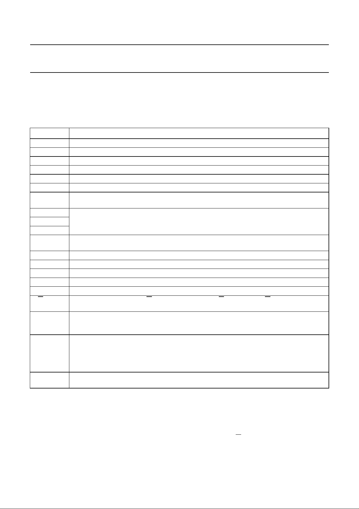
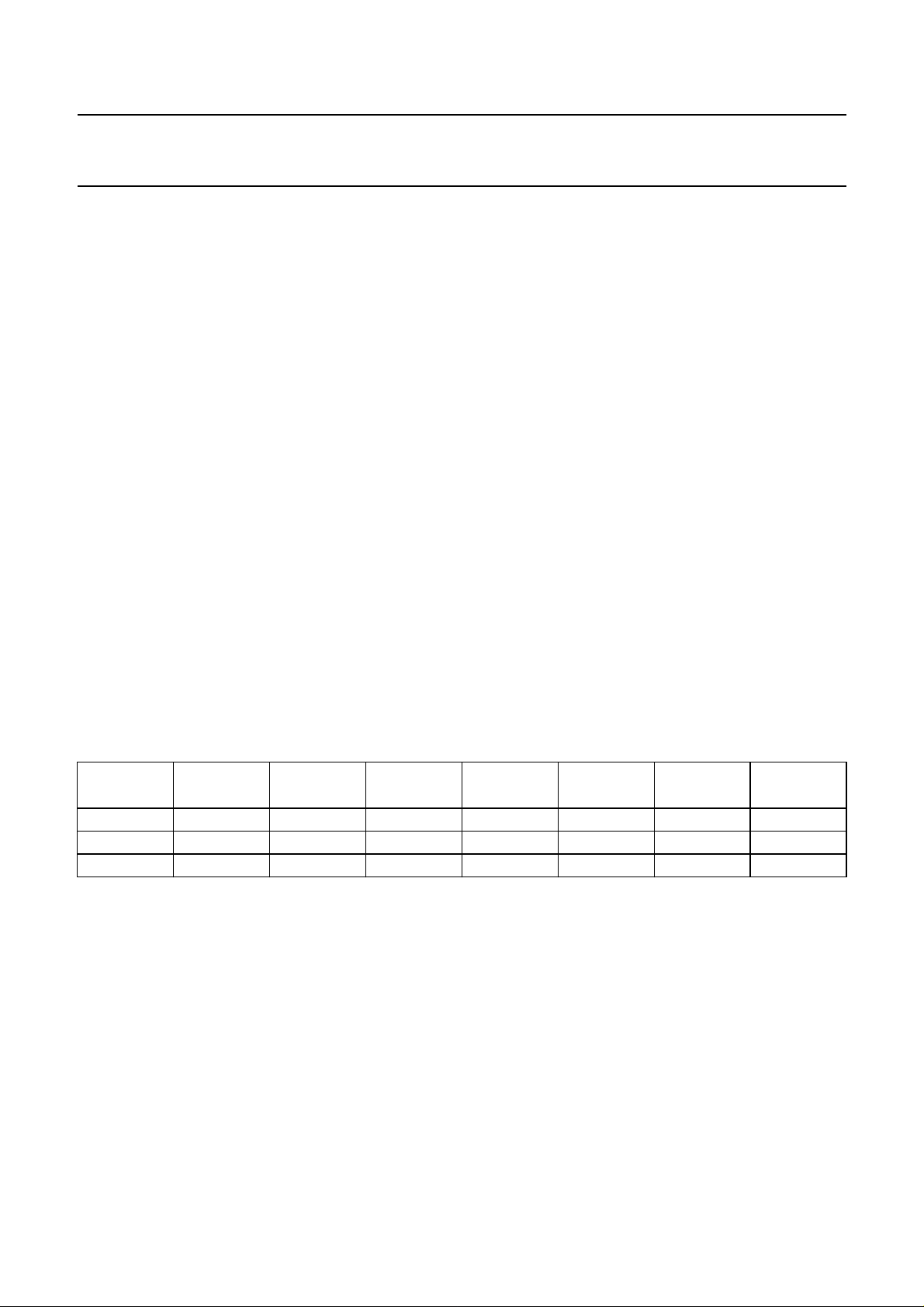
7.12 Character Generator ROM (CGROM)
The Character Generator ROM generates 240 character
patterns in a 5 × 8 dot format from 8-bit character codes.
Figure 6 shows the character set that is currently
implemented.
7.13 Character Generator RAM (CGRAM)
Up to 16 user defined characters may be stored in the
Character Generator RAM. Some CGRAM characters
(see Fig.17) are also used to drive icons (6 if icons blink
and both icon rows are used in the application; 3 if no blink
but both icon rows are used in the application; 0 if no icons
are driven by the icon rows). The CGROM and CGRAM
use a common address space, of which the first column is
reserved for the CGRAM (see Fig.6). Figure 9 shows the
addressing principle for the CGRAM.
7.14 Cursor control circuit
The cursor control circuit generates the cursor (underline
and/or cursor blink as shown in Fig.5) at the DDRAM
address contained in the address counter.
When the address counter contains the CGRAM address
the cursor will be inhibited.
7.15 Timing generator
The timing generator produces the various signals
required to drive the internal circuitry. Internal chip
operation is not disturbed by operations on the data buses.
7.16 LCD row and column drivers
The PCF2119x contains 18 row and 80 column drivers,
which connect the appropriate LCD bias voltages in
sequence to the display in accordance with the data to be
displayed. R17 and R18 drive the icon rows.
The bias voltages and the timing are selected
automatically when the number of lines in the display is
selected. Figures 10 to 13 show typical waveforms.
Unused outputs should be left unconnected.
cursor
5 x 7 dot character font alternating display
cursor display example blink display example
Fig.5 Cursor and blink display examples.
1999 Mar 02 9
MGA801
Philips Semiconductors Product specification
LCD controllers/drivers PCF2119x
handbook, full pagewidth
lower
4 bits
xxxx 0000
xxxx 0001
xxxx 0010
xxxx 0011
xxxx 0100
xxxx 0101
xxxx 0110
xxxx 0111
upper
4 bits
0001 0010 0011 0100 0101 0110 0111 1000 1001 1010 1011 1100 1101 1110 11110000
1
2
3
4
5
6
7
8
xxxx 1000
xxxx 1001
xxxx 1010
xxxx 1011
xxxx 1100
xxxx 1101
xxxx 1110 15
xxxx 1111 16
10
11
12
13
14
9
MGL535
Fig.6 Character set ‘R’ in CGROM.
1999 Mar 02 10
Philips Semiconductors Product specification
LCD controllers/drivers PCF2119x
handbook, full pagewidth
lower
4 bits
xxxx 0000
xxxx 0001
xxxx 0010
xxxx 0011
xxxx 0100
xxxx 0101
xxxx 0110
xxxx 0111
upper
4 bits
0001 0010 0011 0100 0101 0110 0111 1000 1001 1010 1011 1100 1101 1110 11110000
1
2
3
4
5
6
7
8
xxxx 1000
xxxx 1001
xxxx 1010
xxxx 1011
xxxx 1100
xxxx 1101
xxxx 1110
xxxx 1111
9
10
11
12
13
14
15
16
MGL534
Fig.7 Character set ‘S’ in CGROM.
1999 Mar 02 11

Philips Semiconductors Product specification
LCD controllers/drivers PCF2119x
handbook, full pagewidth
lower
4 bits
xxxx 0000
xxxx 0001
xxxx 0010
xxxx 0011
xxxx 0100
xxxx 0101
xxxx 0110
xxxx 0111
upper
4 bits
0001 0010 0011 0100 0101 0110 0111 1000 1001 1010 1011 1100 1101 1110 11110000
1
2
3
4
5
6
7
8
xxxx 1000
xxxx 1001
xxxx 1010
xxxx 1011
xxxx 1100
xxxx 1101
xxxx 1110
xxxx 1111
9
10
11
12
13
14
15
16
MGL597
Fig.8 Character set ‘V’ in CGROM.
1999 Mar 02 12

Philips Semiconductors Product specification
LCD controllers/drivers PCF2119x
handbook, full pagewidth
character codes
(DDRAM data)
76543210 6543210 43210
higher
order
bits
00000000 0000000 0
00000001 0001
00000010
00001111
00001111
00001111
00001111
lower
order
bits
CGRAM
address
higher
order
bits
010 0000
1
1
1
1
1
1
1
1
1
111
1
1
lower
order
bits
001 000
010 000
011 0
100 0 00
101 00 0
110 000
111 00000
000 000
001 0 0 0
010
100
101 00 00
110 00 00
111 00000
001
1
100
1
101
1
110
1
1
higher
order
bits
character patterns
(CGRAM data)
00 00011
lower
order
bits
character
pattern
example 1
cursor
position
character
pattern
example 2
character code
(CGRAM data)
43210
1
111
1
000
1
000
1111
0010
1
00 01
1
000
1
00
1
000
0
101
1
111
0100
1111
1
01 00
0
010
0
00
0
1
1
0
1
000
1
0
1
0
0
000
MGE995
Character code bits 0to 3 correspond to CGRAM address bits 3 to 6.
CGRAM address bits 0 to 2 designate the character pattern line position. The 8th line is the cursor position and display is performed by logical OR with
the cursor. Data in the 8th position will appear in the cursor position.
Character pattern column positions correspond to CGRAM data bits 0 to 4, as shown in Fig.6.
As shown in Figs 6 and 7, CGRAM character patterns are selected when character code bits 4 to 7 are all logic 0. CGRAM data = logic 1 corresponds
to selection for display.
Only bits 0 to 5 of the CGRAM address are set by the ‘set CGRAM address’ command. Bit 6 can be set using the ‘set DDRAM address’ command in
the valid address range or by using the auto-increment feature during CGRAM write. All bits 0 to6 can be read using the ‘read busy flag and address
counter’ command.
Fig.9 Relationship between CGRAM addresses, data and display patterns.
1999 Mar 02 13

Philips Semiconductors Product specification
LCD controllers/drivers PCF2119x
handbook, full pagewidth
V
LCD
V
2
ROW 1
ROW 9
ROW 2
COL1
COL2
V3/V
V
5
V
SS
V
LCD
V
2
V3/V
V
5
V
SS
V
LCD
V
2
V3/V
V
5
V
SS
V
LCD
V
2
V3/V
V
5
V
SS
V
LCD
V
2
V3/V
V
5
V
SS
frame n + 1 frame n
state 1 (ON)
state 2 (OFF)
R1
4
R2
R3
R4
R5
R6
R7
R8
4
R9
4
4
4
V
OP
0.5V
OP
0.25V
OP
0 V
state 1
−0.25V
OP
−0.5V
OP
−V
OP
V
OP
0.5V
OP
0.25V
OP
0 V
state 2
−0.25V
OP
−0.5V
OP
−V
OP
123 18123 18
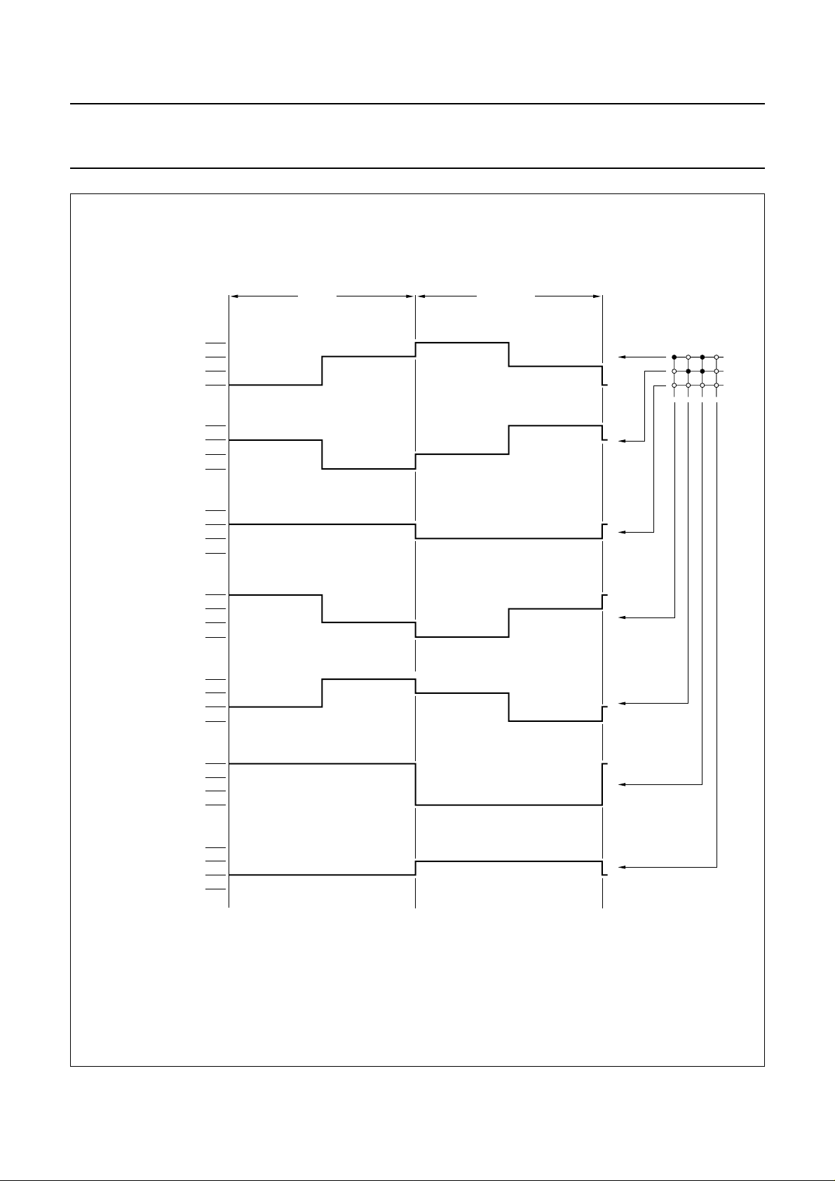
Fig.10 MUX 1 : 18 LCD waveforms; character mode.
1999 Mar 02 14
MGE996

Philips Semiconductors Product specification
LCD controllers/drivers PCF2119x
handbook, full pagewidth
V
LCD
V
2
ROW 1
ROW 2
ROW 3
COL1
COL2
V3/V
V
5
V
SS
V
LCD
V
2
V3/V
V
5
V
SS
V
LCD
V
2
V3/V
V
5
V
SS
V
LCD
V
2
V3/V
V
5
V
SS
V
LCD
V
2
V3/V
V
5
V
SS
frame n + 1 frame n
state 1 (ON)
state 2 (OFF)
R1
4
R2
R3
R4
R5
R6
R7
R8
4
R9
4
4
4
V
OP
0.5V
OP
0.25V
OP
0 V
state 1
−0.25V
OP
−0.5V
OP
−V
OP
V
OP
0.5V
OP
0.25V
OP
0 V
state 2
−0.25V
OP
−0.5V
OP
−V
OP
1919
Fig.11 MUX1:9 LCD waveforms; character mode. R10 to 18 to be left open.
1999 Mar 02 15
MGK900
Philips Semiconductors Product specification
LCD controllers/drivers PCF2119x
handbook, full pagewidth
ROW 17
ROW 18
ROW 1 to 16
COL 1
ON/OFF
COL 2
OFF
/ON
V
V
V
V
V
LCD
2/3
1/3
V
SS
LCD
2/3
1/3
V
SS
LCD
2/3
1/3
V
SS
LCD
2/3
1/3
V
SS
LCD
2/3
1/3
V
SS
frame n + 1 frame n
only icons are
driven (MUX 1 : 2)
V
LCD
V
2/3
1/3
V
SS
LCD
2/3
1/3
V
SS
COL 3
COL 4
ON/ON
OFF/OFF
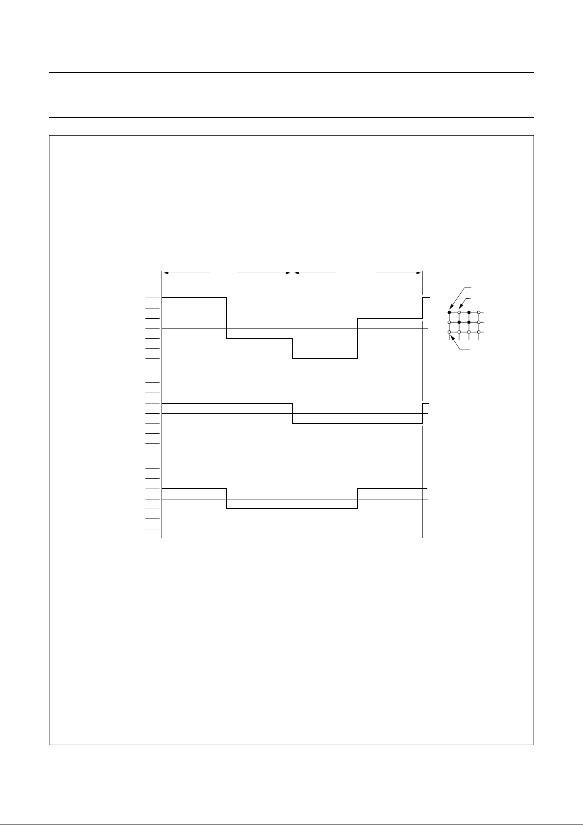
Fig.12 MUX 1 : 2 LCD waveforms; icon mode.
1999 Mar 02 16
MGE997
Philips Semiconductors Product specification
LCD controllers/drivers PCF2119x
handbook, full pagewidth
state 1
COL 1 -
ROW 17
state 2
COL 2 -
ROW 17
state 3
COL 1 -
ROW 1 to 16
V
2/3 V
1/3 V
−1/3 V
−2/3 V
−V
2/3 V
1/3 V
−1/3 V
−2/3 V
−V
2/3 V
1/3 V
−1/3 V
−2/3 V
−V
PIXEL
V
OP
OP
OP
OP
OP
OP
V
OP
OP
OP
OP
OP
OP
V
OP
OP
OP
OP
OP
OP
frame n + 1 frame n
state 1 (ON)
state 2 (OFF)
R17
0
R18
R1-16
state 3 (OFF)
0
0
MGE998
V
= 0.745V
ON(rms)
V
OFF(rms)
D
V
ON
------------V
OFF
= 0.333V
2.23==
OP
OP
Fig.13 MUX 1 : 2 LCD waveforms; icon mode.
1999 Mar 02 17

Philips Semiconductors Product specification
LCD controllers/drivers PCF2119x
7.17 Reset function
The PCF2119x must be reset externally when power is turned on. The reset executes a ‘clear display’, requiring
165 oscillator cycles. After the reset the chip has the state shown in Table 4.
Table 4 State after reset
STEP FUNCTION CONTROL BIT STATE CONDITION
1 clear display
2 entry mode set I/D = 1 +1 (increment)
S = 0 no shift
3 display control D = 0 display off
C = 0 cursor off
B = 0 cursor character blink off
4 function set DL = 1 8-bit interface
M = 0 1-line display
H = 0 normal instruction set
SL = 0 MUX 1 : 18 mode
5 default address pointer to DDRAM; the Busy Flag (BF) indicates the busy state (BF = 1) until
initialization ends; the busy state lasts 2 ms; the chip may also be initialized by software; see
Tables 17 and 18
6 icon control IM, IB = 00 icons/icon blink disabled
7 display/screen configuration L = 0; P = 0; Q = 0 default configurations
8V
9 set V
10 I
temperature coefficient TC1 = 0; TC2 = 0 default temperature coefficient
LCD
LCD
2
C-bus interface reset
VA= 0; VB= 0 (V
generator off)
LCD
1999 Mar 02 18
 Loading...