


查询PCF2119X供应商
INTEGRATED CIRCUITS
DATA SH EET
PCF2119X
LCD controllers/drivers
Product specification
Supersedes data of 2002 Jan 16
2003 Jan 30

Philips Semiconductors Product specification
LCD controllers/drivers PCF2119X
CONTENTS
1 FEATURES
1.1 Note
2 APPLICATIONS
3 GENERAL DESCRIPTION
4 ORDERING INFORMATION
5 BLOCK DIAGRAM
6 PAD INFORMATION
6.1 Pad functions
7 FUNCTIONAL DESCRIPTION
7.1 LCD supply voltage generator
7.2 Programming ranges
7.3 LCD bias voltage generator
7.4 Oscillator
7.5 External clock
7.6 Power-on reset
7.7 Power-down mode
7.8 Registers
7.9 Busy flag
7.10 Address Counter (AC)
7.11 Display Data RAM (DDRAM)
7.12 Character Generator ROM (CGROM)
7.13 Character Generator RAM (CGRAM)
7.14 Cursor control circuit
7.15 Timing generator
7.16 LCD row and column drivers
7.17 Reset function
8 INSTRUCTIONS
8.1 Clear display
8.2 Return home
8.3 Entry mode set
8.4 Display control (and partial power-down mode)
8.5 Cursor or display shift
8.6 Function set
8.7 Set CGRAM address
8.8 Set DDRAM address
8.9 Read busy flag and read address
8.10 Write data to CGRAM or DDRAM
8.11 Read data from CGRAM or DDRAM
9 EXTENDED FUNCTION SET
INSTRUCTIONS AND FEATURES
9.1 New instructions
9.2 Icon control
9.3 IM
9.4 IB
9.5 Normal/icon mode operation
9.6 Direct mode
9.7 Voltage multiplier control
9.8 Screen configuration
9.9 Display configuration
9.10 TC1 and TC2
9.11 Set V
9.12 Reducing current consumption
10 INTERFACES TO MPU
10.1 Parallel interface
10.2 I2C-bus interface
11 LIMITING VALUES
12 HANDLING
13 DC CHARACTERISTICS
14 AC CHARACTERISTICS
15 TIMING CHARACTERISTICS
16 APPLICATION INFORMATION
16.1 General information
16.2 Charge pump characteristics
16.3 8-bit operation, 1-line display using external
16.4 4-bit operation, 1-line display using external
16.5 8-bit operation, 2-line display
16.6 I2C-bus operation, 1-line display
17 DEVICE PROTECTION DIAGRAMS
18 BONDING PAD LOCATIONS
19 DATA SHEET STATUS
20 DEFINITIONS
21 DISCLAIMERS
22 PURCHASE OF PHILIPS I2C COMPONENTS
LCD
reset
reset
2003 Jan 30 2

Philips Semiconductors Product specification
LCD controllers/drivers PCF2119X
1 FEATURES
• Single-chip LCD controller/driver
• 2-line display of up to 16 characters + 160 icons, or
1-line display of up to 32 characters + 160 icons
• 5 × 7 character format plus cursor; 5 × 8 for kana
(Japanese) and user defined symbols
• Icon mode: reduced current consumption while
displaying icons only
• Icon blink function
• On-chip:
– Configurable 4 (3 and 2) times voltage multiplier
generating LCD supplyvoltage, independent of VDD,
programmable by instruction (external supply also
possible)
– Temperature compensation of on-chip generated
V
: −0.16 to −0.24 %/K (programmable by
LCD
instruction)
– Generation of intermediate LCD bias voltages
– Oscillator requires no external components (external
clock also possible).
• Display Data RAM: 80 characters
• Character Generator ROM: 240, 5 × 8 characters
• Character Generator RAM: 16, 5 × 8 characters;
4 characters used to drive 160 icons, 8 characters used
if icon blink feature is used in application
• 4 or 8-bit parallel bus and 2-wire I2C-bus interface
• CMOS compatible
• 18 row and 80 column outputs
• Multiplex rates 1 : 18 (for normal operation), 1 : 9 (for
single line operation) and 1 : 2 (for icon only mode)
• Uses common 11 code instruction set (extended)
• Logic supply voltage range, V
− VSS= 1.5 to 5.5 V
DD1
(chip may be driven with two battery cells)
• Display supply voltage range, V
• HVgen supply voltage range, V
and V
− VSS= 2.2 to 4 V
DD3
− VSS= 2.2 to 6.5 V
LCD
− VSS= 2.2 to 4 V
DD2
• Direct mode to save current consumption for icon mode
and Mux 1 : 9 (depending on V
value and LCD liquid
DD2
properties)
• Very low current consumption (20 to 200 µA):
– Icon mode: <25 µA
– Power-down mode: <2 µA.
1.1 Note
Icon mode is used to save current. When only icons are
displayed, a much lower operating voltage V
LCD
can be
used and the switching frequency of the LCD outputs is
reduced. In most applications it is possible to use VDD as
V
.
LCD
2 APPLICATIONS
• Telecom equipment
• Portable instruments
• Point-of-sale terminals.
3 GENERAL DESCRIPTION
The PCF2119x is a low power CMOS LCD controller and
driver, designed to drive a dot matrix LCD display of 2-line
by 16 or 1-line by 32 characters with 5 × 8 dot format. All
necessaryfunctionsforthedisplay are provided in a single
chip, including on-chip generation of LCD bias voltages,
resulting in a minimum of external components and lower
system current consumption. The PCF2119x interfaces to
most microcontrollers via a 4 or 8-bit bus or via the 2-wire
I2C-bus. The chip contains a character generator and
displays alphanumeric and kana (Japanese) characters.
The letter ‘x’ in PCF2119x characterizes the built-in
characterset.Variouscharactersetscanbe manufactured
on request.
2003 Jan 30 3
Philips Semiconductors Product specification
LCD controllers/drivers PCF2119X
4 ORDERING INFORMATION
TYPE NUMBER
NAME DESCRIPTION VERSION
PCF2119AU/2 − chip with bumps in tray 2
PCF2119DU/2 − chip with bumps in tray 2
PCF2119FU/2 − chip with bumps in tray 2
PCF2119RU/2 − chip with bumps in tray 2
PCF2119SU/2 − chip with bumps in tray 2
PCF2119VU/2 − chip with bumps in tray 2
PACKAGE
2003 Jan 30 4
Philips Semiconductors Product specification
LCD controllers/drivers PCF2119X
5 BLOCK DIAGRAM
handbook, full pagewidth
V
LCD1
V
LCD2
V
LCDSENSE
V
DD1
V
DD2
V
DD3
V
SS1
V
SS2
44 to 49
37 to 43
36
1 to 6
7 to 14
15 to 18
22 to 29
30 to 35
BIAS
VOLT AGE
GENERATOR
V
LCD
GENERATOR
SHIFT REGISTER 5 × 12 BIT
CURSOR AND DATA CONTROL
CHARACTER
GENERATOR
RAM (128 × 5)
(CGRAM)
16 CHARACTERS
C1 to C80 R17DUP R1 to R18
60 to 99,
101 to 140
80
COLUMN DRIVERS
80
DATA LATCHES
80
5
5
CHARACTER
GENERATOR
ROM
(CGROM)
240 CHARACTERS
8
100
SHIFT REGISTER 18-BIT
51 to 59,
141 to 149
18
ROW DRIVERS
18
OSCILLATOR
TIMING
GENERATOR
168
OSC
T1
T2
T3
DB3/SA0
20
21
153
163
DATA
REGISTER
(DR)
161 to 162
DB1 to DB2
7
8
BUSY
FLAG
164 to 167
DB4 to DB7
DISPLAY DATA RAM
(DDRAM)
80 CHARACTERS/BYTES
ADDRESS COUNTER
INSTRUCTION
DECODER
INSTRUCTION
REGISTER
I/O BUFFER
E
R/W
Fig.1 Block diagram.
(AC)
RS
155
PD
7
77
8
7
DISPLAY
ADDRESS
COUNTER
PCF2119x
154
8
156,
151,
15915819
SCL
152
157
MGW571
SDA
POR
2003 Jan 30 5
Philips Semiconductors Product specification
LCD controllers/drivers PCF2119X
6 PAD INFORMATION
The identification of each pad and its location is given in Chapter 18.
6.1 Pad functions
Table 1 Pad function description
SYMBOL DESCRIPTION
V
DD1
, V
V
DD2
DD3
V
SS1
V
SS2
V
LCD1
V
LCD2
V
LCDSENSE
E The data bus clock input is set HIGH to signal the start of a read or write operation; data is clocked in
T1 to T3 These are three test pads. T1 and T2 must be connected to V
R1 to R18;
R17DUP
C1 to C80 LCD column driver outputs C1 to C80.
SCL I
POR External power-on reset input.
PD PD selects the chip power-down mode; for normal operation PD = 0.
SDA I
W This is the read/write input. R/W selects either the read (R/W = 1) or write (R/W = 0) operation. This
R/
RS The RS input selects the register to be accessed for read and write. RS = 0, selects the instruction
DB0 to DB7 The 8-bit bidirectional data bus (3-state) transfers data between the system controller and the
OSC Oscillator or external clock input. When the on-chip oscillator is used this pad must be connected to
Logic supply voltage.
High voltage generator supply voltages (always put V
DD2=VDD3
).
This is the ground pad for all except the high voltage generator.
This is the ground pad for the high voltage generator.
This input is used for the generation of the LCD bias levels.
This is the V
The pad must be left open-circuit when V
This input (V
V
when using internal LCD supply and to V
LCD2
output pad if V
LCD
) is used for the voltage multiplier’s regulation circuitry. This pad must be connected to
LCD
is generated internally then pad V
LCD
is generated externally.
LCD
and V
LCD1
LCD2
must be connected to V
LCD2
when using external LCD supply.
LCD1
or out of the chip on the negative edge of the clock; note 1.
; T3 is left open-circuit and is not user
SS1
accessible.
LCD row driver outputs R1 to R18; these pads output the row select waveforms to the display;
R17 and R18 drive the icons. R17 has two pads R17 and R17DUP.
2
C-bus serial clock input; note 1.
2
C-bus serial data input/output; note 1.
pad has an internal pull-up resistor.
register for write and the busy flag and address counter for read. RS = 1, selects the data register for
both read and write. This pad has an internal pull-up resistor.
PCF2119x. DB7 may be used as the busy flag, signalling that internal operations are not yet
completed. In 4-bit operations the 4 higher order lines DB7 to DB4 are used; DB3 to DB0 must be left
2
open-circuit. Data bus line DB3 has an alternative function (SA0), when selected this is the I
C-bus
address pad. Each data line has its own internal pull-up resistor; note 1.
V
DD1.
.
Note
2
1. When the I
DB2 to DB0 should be connected to V
a) When the parallel bus is used, pads SCL and SDA must be connected to V
C-bus is used, the parallel interface pad E must be at logic 0. In the I2C-bus read mode DB7 to DB4 and
or left open-circuit.
DD1
SS1
or V
; they must not be left
DD1
open-circuit.
b) If the 4-bit interface is used without reading out from the PCF2119x (i.e. R/W is set permanently to logic 0), the
unused ports DB0 to DB4 can either be set to V
SS1
or V
instead of leaving them open-circuit.
DD1
2003 Jan 30 6

Philips Semiconductors Product specification
LCD controllers/drivers PCF2119X
7 FUNCTIONAL DESCRIPTION
7.1 LCD supply voltage generator
The LCD supply voltage may be generated on-chip. The
voltage generator is controlled by two internal 6-bit
registers: VAand VB. The nominal LCD operating voltage
at room temperature is given by the relationship:
V
OP(nom)
integer value of register 0.08×()1.82+=
7.2 Programming ranges
Programmed value: 1 to 63. Voltage: 1.90 to 6.86 V.
=27°C.
T
ref
Values producing more than 6.5 V at operating
temperature are not allowed. Operation above this
voltage may damage the device. When programming the
operating voltage the V
temperature coefficient must
LCD
be taken into account.
Values below 2.2 V are below the specified operating
range of the chip and are therefore not allowed.
Value 0 for VA and VB switches the generator off
(i.e. VA= 0 in character mode, VB= 0 in icon mode).
Usually register VA is programmed with the voltage for
character mode and register VB with the voltage for icon
mode.
When the generator and the direct mode are switched off
an external voltage may be supplied at connected pads
. V
V
LCD1
may be higher or lower than VDD.
LCD1
During direct mode (program DM register bit) the internal
voltagegenerator is turned off and the V
is directly connected to V
. This reduces the current
DD2
outputvoltage
LCD
consumption during icon mode and Mux 1 : 9 (depending
on the V
value and the LCD liquid properties).
DD2
TheLCD supply voltage generatorensuresthat,as long as
VDD is in the valid range (2.2 to 4 V), the required peak
voltage VOP= 6.5 V can be generated at any time.
7.3 LCD bias voltage generator
The intermediate bias voltages for the LCD display are
also generated on-chip. This removes the need for an
external resistive bias chain and significantly reduces the
system current consumption. The optimum value of V
LCD
depends on the multiplex rate, the LCD threshold voltage
(Vth) and the number of bias levels. Using a 5-level bias
scheme for 1 : 18 maximum rate allows V
LCD
< 5 V for
most LCD liquids. The intermediate bias levels for the
different multiplex rates are shown in Table 2. These bias
levels are automatically set to the given values when
switching to the corresponding multiplex rate.
When V
is generated on-chip the V
LCD
pads should be
LCD
decoupled to VSSwith a suitable capacitor. The generated
V
is independent of VDD and is temperature
LCD
compensated.
Table 2 Bias levels as a function of multiplex rate
MULTIPLEX
RATE
1:18 5 V
1:9 5 V
1:2 4 V
NUMBER
OF LEVELS
V
1
op
op
op
V
2
(1)
3/4
3/4 1/2 1/2 1/4 V
2/3 2/3 1/3 1/3 V
Note
1. The values in the above table are given relative to V
V
3
V
4
1/2 1/2 1/4 V
− Vss, e.g. 3/4 means 3/4 × (Vop− Vss).
op
V
5
V
6
ss
ss
ss
2003 Jan 30 7

Philips Semiconductors Product specification
LCD controllers/drivers PCF2119X
7.4 Oscillator
The on-chip oscillator provides the clock signal for the
display system. No external components are required and
the OSC pad must be connected to VDD.
7.5 External clock
If an external clock is to be used this is input at the OSC
pad. The resulting display frame frequency is given by:
f
=
OSC
------------3072
f
frame
Only in the power-down state is the clock allowed to be
stopped (OSC connected to V
), otherwise the LCD is
SS
frozen in a DC state.
7.6 Power-on reset
ThePCF2119xmustbereset externally. This is an internal
synchronous reset that requires 3 OSC cycles to be
executed after release of the external reset signal. If no
external reset is performed, the chip might start-up in an
unwanted state. The external reset is active HIGH.
7.7 Power-down mode
The chip can be put into power-down mode by applying an
external active HIGH level to the PD pad. In power-down
mode all static currents are switched off (no internal
oscillator, no bias level generation and all LCD outputs are
internally connected to V
SS
).
During power-down, information in the RAMs and the chip
state are preserved. Instruction execution during
power-down is possible when pad OSC is externally
clocked.
7.8 Registers
The instruction register can be written to but not read from
by the system controller. The data register temporarily
stores data to be read from the DDRAM and CGRAM.
When reading, data from the DDRAM or CGRAM
corresponding to the address in the instruction register is
written to the data register prior to being read by the ‘read
data’ instruction.
7.9 Busy flag
The busy flag indicates the internal status of the
PCF2119x. A logic 1 indicates that the chip is busy and
further instructions will not be accepted. The busy flag is
output to pad DB7 when RS = 0 and R/
W = 1. Instructions
should only be written after checking that the busy flag is
at logic 0 or waiting for the required number of cycles.
7.10 Address Counter (AC)
The address counter assigns addresses to the DDRAM
and CGRAM for reading and writing and is set by the
commands ‘set CGRAM address’ and ‘set DDRAM
address’. After a read/write operation the address counter
is automatically incremented or decremented by 1. The
address counter contents are output to the bus
(DB6 to DB0) when RS = 0 and R/W=1.
7.11 Display Data RAM (DDRAM)
The DDRAM stores up to 80 characters of display data
represented by 8-bit character codes. RAM locations
which are not used for storing display data can be used as
general purpose RAM. The basic RAM to display
addressing scheme is shown in Fig.2. With no display shift
the characters represented by the codes in the first
32 RAM locations starting at address 00H in line 1 are
displayed. Figures 3 and 4 show the display mapping for
right and left shift respectively.
The PCF2119x has two 8-bit registers, an Instruction
Register (IR) and a Data Register (DR). The Register
Select signal (RS) determines which register will be
accessed.Theinstructionregister stores instruction codes
such as ‘display clear’ and ‘cursor shift’, and address
information for the Display Data RAM (DDRAM) and
Character Generator RAM (CGRAM).
When data is written to or read from the DDRAM
wrap-around occurs from the end of one line to the start of
the next line. When the display is shifted each line wraps
around within itself, independently of the others. Thus all
lines are shifted and wrapped around together. The
address ranges and wrap-around operations for the
various modes are shown in Table 3.
Table 3 Address space and wrap-around operation
MODE 1 × 32 2 × 16 1 × 9
Address space 00 to 4F 00 to 27; 40 to 67 00 to 27
Read/write wrap-around (moves to next line) 4F to 00 27 to 40; 67 to 00 27 to 00
Display shift wrap-around (stays within line) 4F to 00 27 to 00; 67 to 40 27 to 00
2003 Jan 30 8
Philips Semiconductors Product specification
LCD controllers/drivers PCF2119X
handbook, full pagewidth
display
position
DDRAM
address
12345 303132
00 01 02 03 04 1D 1E 1F 20 21 4C 4D 4E 4F
1-line display
12345 141516
00 01 02 03 04 0D 0E 0F 10 11 24 25 26 27
DDRAM
address
12345 141516
2-line display/MUX 1 : 9 mode
Fig.2 DDRAM to display mapping: no shift.
handbook, halfpage
DDRAM
address
2-line display/MUX 1 : 9 mode
non-displayed DDRAM addresses
non-displayed DDRAM address
1 2 3 4 5 14 15 16
27 00 01 02 03
0C 0D 0E
1 2 3 4 5 10 11 12
67 40 41 42 43
4C 4D 4E
64 65 66 6740 41 42 43 44 4D 4E 4F 50 51
line 1
line 2
MGL536
line 1
line 2
MGK892
Fig.3 DDRAM to display mapping: right shift.
display
handbook, halfpage
position
DDRAM
address
1 2 3 4 5 30 31 32
01 04 05
02 03 1E 1F 20
1-line display
1 2 3 4 5 14 15 16
02 03
DDRAM
address
01 04 05
1 2 3 4 5 14 15 16
41 42 43 44 45
2-line display/MUX 1 : 9 mode
Fig.4 DDRAM to display mapping; left shift.
2003 Jan 30 9
0E 0F 10
4E 4F 50
line 1
line 2
MGK894
Philips Semiconductors Product specification
LCD controllers/drivers PCF2119X
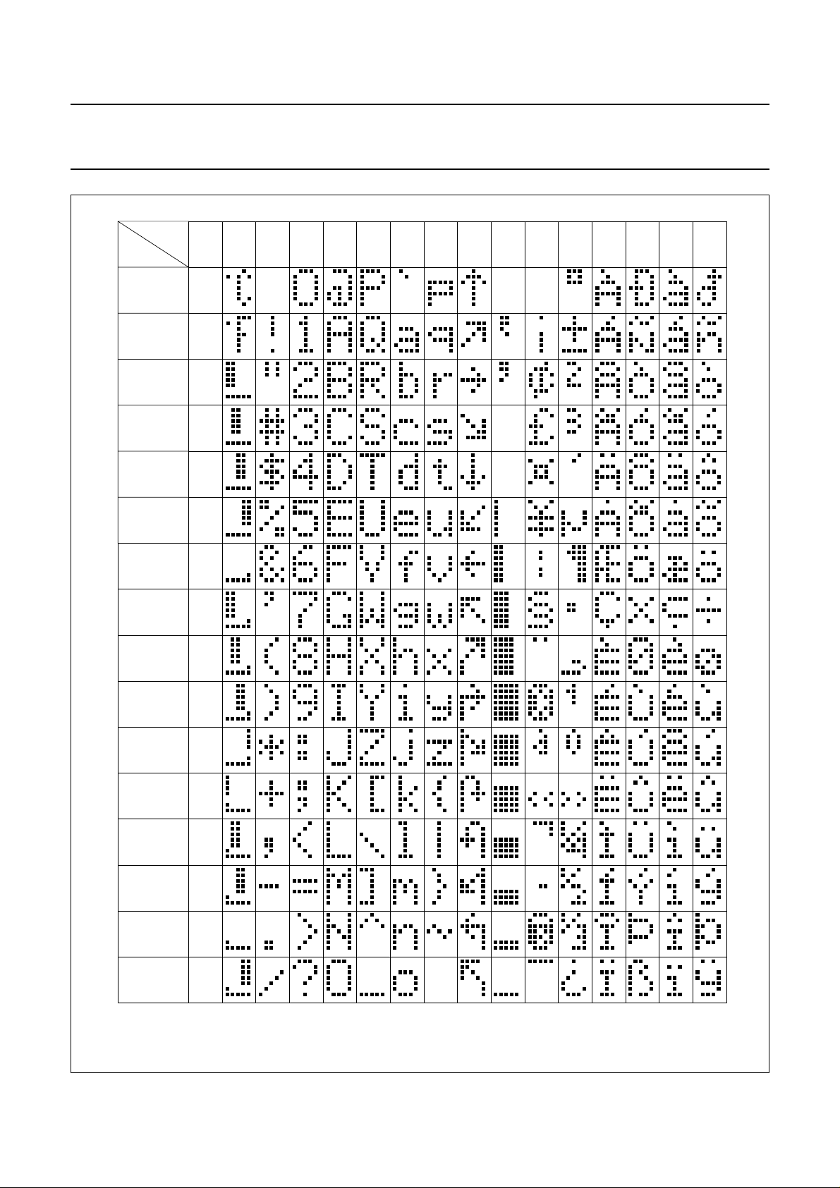
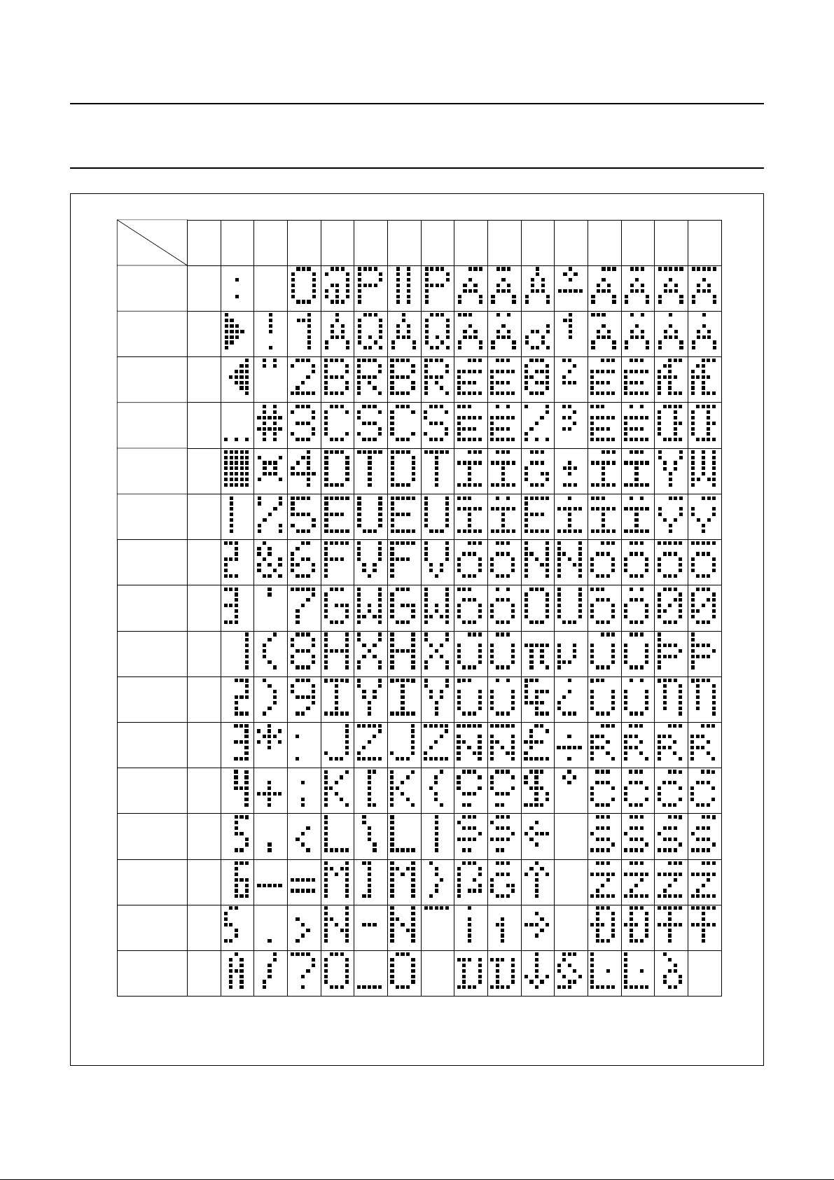
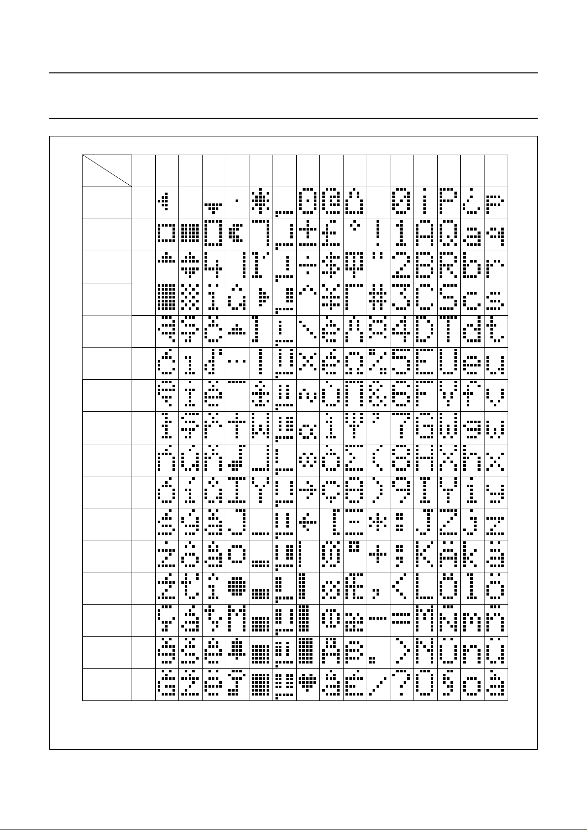
7.12 Character Generator ROM (CGROM)
The Character Generator ROM generates 240 character
patterns in a 5 × 8 dot format from 8-bit character codes.
Figures 6 to 10shows the character sets that are currently
implemented.
7.13 Character Generator RAM (CGRAM)
Up to 16 user defined characters may be stored in the
Character Generator RAM. Some CGRAM characters
(see Fig.19) are also used to drive icons (6 if icons blink
and both icon rows are used in the application; 3 if no blink
but both icon rows are used in the application; 0 if no icons
are driven by the icon rows). The CGROM and CGRAM
use a common address space, of which the first column is
reserved for the CGRAM (see Fig.6 to Fig.10). Figure 11
shows the addressing principle for the CGRAM.
7.14 Cursor control circuit
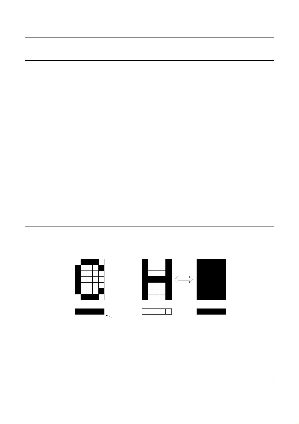
The cursor control circuit generates the cursor (underline
and/or cursor blink as shown in Fig.5) at the DDRAM
address contained in the address counter.
When the address counter contains the CGRAM address
the cursor will be inhibited.
7.15 Timing generator
The timing generator produces the various signals
required to drive the internal circuitry. Internal chip
operation is not disturbed by operations on the data buses.
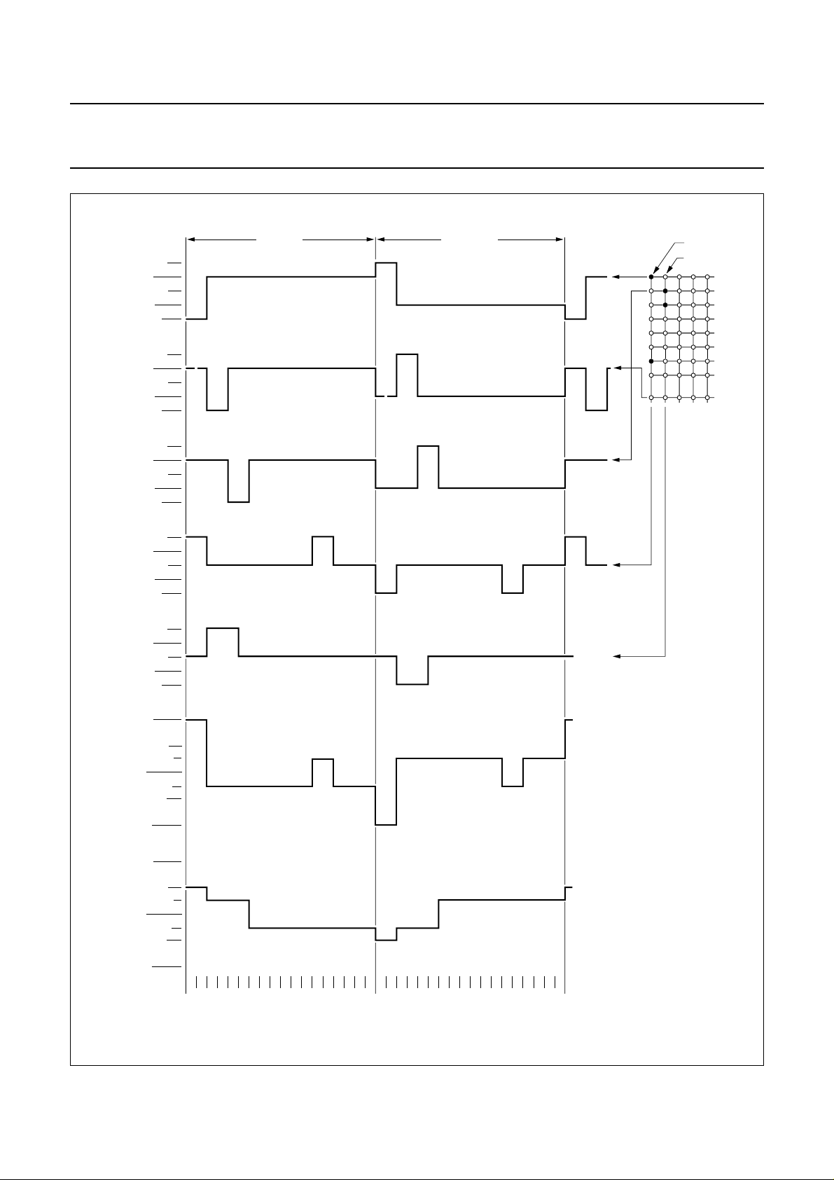
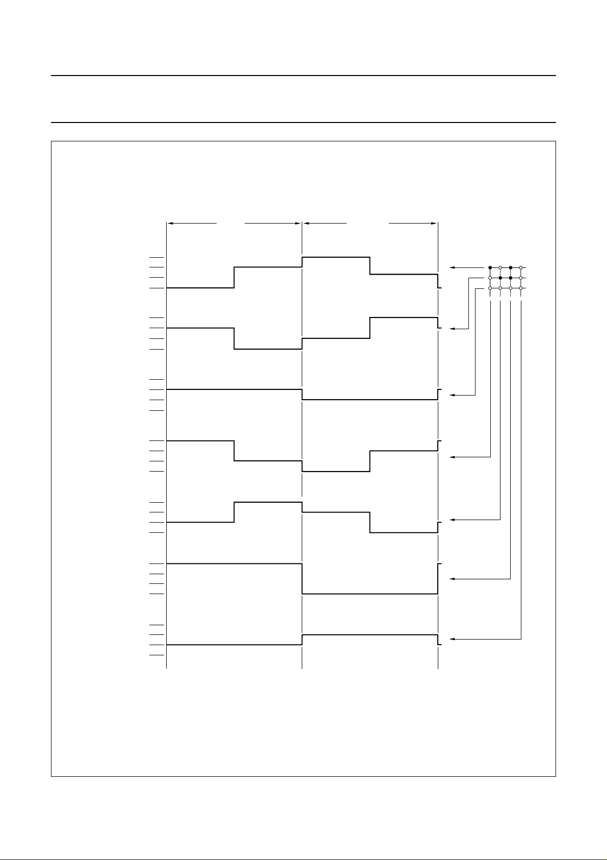
7.16 LCD row and column drivers
The PCF2119x contains 18 row and 80 column drivers,
which connect the appropriate LCD bias voltages in
sequence to the display in accordance with the data to be
displayed. R17 and R18 drive the icon rows.
The bias voltages and the timing are selected
automatically when the number of lines in the display is
selected. Figures 12 to 15 show typical waveforms.
Unused outputs should be left unconnected.
cursor
5 x 7 dot character font alternating display
cursor display example blink display example
Fig.5 Cursor and blink display examples.
2003 Jan 30 10
MGA801
Philips Semiconductors Product specification
LCD controllers/drivers PCF2119X
handbook, full pagewidth
lower
4 bits
xxxx 0000
xxxx 0001
xxxx 0010
xxxx 0011
xxxx 0100
xxxx 0101
xxxx 0110
xxxx 0111
upper
4 bits
0001 0010 0011 0100 0101 0110 0111 1000 1001 1010 1011 1100 1101 1110 11110000
1
2
3
4
5
6
7
8
xxxx 1000
xxxx 1001
xxxx 1010
xxxx 1011
xxxx 1100
xxxx 1101
xxxx 1110 15
xxxx 1111 16
9
10
11
12
13
14
MCE190
Fig.6 Character set ‘A’ in CGROM.
2003 Jan 30 11
Philips Semiconductors Product specification
LCD controllers/drivers PCF2119X
handbook, full pagewidth
lower
4 bits
xxxx 0000
xxxx 0001
xxxx 0010
xxxx 0011
xxxx 0100
xxxx 0101
xxxx 0110
xxxx 0111
upper
4 bits
0001 0010 0011 0100 0101 0110 0111 1000 1001 1010 1011 1100 1101 1110 11110000
1
2
3
4
5
6
7
8
xxxx 1000
xxxx 1001
xxxx 1010
xxxx 1011
xxxx 1100
xxxx 1101
xxxx 1110 15
xxxx 1111 16
9
10
11
12
13
14
MCE173
Fig.7 Character set ‘D’ in CGROM.
2003 Jan 30 12
Philips Semiconductors Product specification
LCD controllers/drivers PCF2119X
handbook, full pagewidth
lower
4 bits
xxxx 0000
xxxx 0001
xxxx 0010
xxxx 0011
xxxx 0100
xxxx 0101
xxxx 0110
xxxx 0111
upper
4 bits
0001 0010 0011 0100 0101 0110 0111 1000 1001 1010 1011 1100 1101 1110 11110000
1
2
3
4
5
6
7
8
xxxx 1000
xxxx 1001
xxxx 1010
xxxx 1011
xxxx 1100
xxxx 1101
xxxx 1110 15
xxxx 1111 16
9
10
11
12
13
14
MGU552
Fig.8 Character set ‘F’ in CGROM.
2003 Jan 30 13
Philips Semiconductors Product specification
LCD controllers/drivers PCF2119X
handbook, full pagewidth
lower
4 bits
xxxx 0000
xxxx 0001
xxxx 0010
xxxx 0011
xxxx 0100
xxxx 0101
xxxx 0110
xxxx 0111
upper
4 bits
0001 0010 0011 0100 0101 0110 0111 1000 1001 1010 1011 1100 1101 1110 11110000
1
2
3
4
5
6
7
8
xxxx 1000
xxxx 1001
xxxx 1010
xxxx 1011
xxxx 1100
xxxx 1101
xxxx 1110 15
xxxx 1111 16
9
10
11
12
13
14
MGL535
Fig.9 Character set ‘R’ in CGROM.
2003 Jan 30 14
Philips Semiconductors Product specification
LCD controllers/drivers PCF2119X
handbook, full pagewidth
lower
4 bits
xxxx 0000
xxxx 0001
xxxx 0010
xxxx 0011
xxxx 0100
xxxx 0101
xxxx 0110
xxxx 0111
upper
4 bits
0001 0010 0011 0100 0101 0110 0111 1000 1001 1010 1011 1100 1101 1110 11110000
1
2
3
4
5
6
7
8
xxxx 1000
xxxx 1001
xxxx 1010
xxxx 1011
xxxx 1100
xxxx 1101
xxxx 1110
xxxx 1111
9
10
11
12
13
14
15
16
MGL534
Fig.10 Character set ‘S’ in CGROM.
2003 Jan 30 15
Philips Semiconductors Product specification
LCD controllers/drivers PCF2119X
handbook, full pagewidth
character codes
(DDRAM data)
76543210 6543210 43210
higher
order
bits
00000000 0000000 0
00000001 0001
00000010
00001111
00001111
00001111
00001111
lower
order
bits
CGRAM
address
higher
order
bits
010 0000
1
1
1
1
1
1
1
1
1
111
1
1
lower
order
bits
001 000
010 000
011 0
100 0 00
101 00 0
110 000
111 00000
000 000
001 0 0 0
010
100
101 00 00
110 00 00
111 00000
001
1
100
1
101
1
110
1
1
higher
order
bits
character patterns
(CGRAM data)
00 00011
lower
order
bits
character
pattern
example 1
cursor
position
character
pattern
example 2
character code
(CGRAM data)
43210
1
111
1
000
1
000
1111
0010
1
00 01
1
000
1
00
1
000
0
101
1
111
0100
1111
1
01 00
0
010
0
00
0
1
1
0
1
000
1
0
1
0
0
000
MGE995
Character code bits 0 to 3 correspond to CGRAM address bits 3 to 6.
CGRAM address bits 0 to 2 designate the character pattern line position. The 8th line is the cursor position and display is performed by logical OR with
the cursor. Data in the 8th position will appear in the cursor position.
Character pattern column positions correspond to CGRAM data bits 0 to 4, as shown in Figs. 7 to 10
As shown in Figs. 7 to 10, CGRAM character patterns are selected when character code bits 4 to 7 are all logic 0. CGRAM data = logic 1 corresponds
to selection for display.
Only bits 0 to 5 of the CGRAM address are set by the ‘set CGRAM address’ command. Bit 6 can be set using the ‘set DDRAM address’ command in
the valid address range or by using the auto-increment feature during CGRAM write. All bits 0 to 6 can be read using the ‘read busy flag and address
counter’ command.
Fig.11 Relationship between CGRAM addresses, data and display patterns.
2003 Jan 30 16
Philips Semiconductors Product specification
LCD controllers/drivers PCF2119X
handbook, full pagewidth
V
LCD
V
2
ROW 1
ROW 9
ROW 2
COL1
COL2
V3/V
V
5
V
SS
V
LCD
V
2
V3/V
V
5
V
SS
V
LCD
V
2
V3/V
V
5
V
SS
V
LCD
V
2
V3/V
V
5
V
SS
V
LCD
V
2
V3/V
V
5
V
SS
frame n + 1 frame n
state 1 (ON)
state 2 (OFF)
R1
4
R2
R3
R4
R5
R6
R7
R8
4
R9
4
4
4
V
OP
0.5V
OP
0.25V
OP
0 V
state 1
−0.25V
OP
−0.5V
OP
−V
OP
V
OP
0.5V
OP
0.25V
OP
0 V
state 2
−0.25V
OP
−0.5V
OP
−V
OP
123 18123 18
Fig.12 MUX 1 : 18 LCD waveforms; character mode.
2003 Jan 30 17
MGE996
Philips Semiconductors Product specification
LCD controllers/drivers PCF2119X
handbook, full pagewidth
V
LCD
V
2
ROW 1
ROW 2
ROW 3
COL1
COL2
V3/V
V
5
V
SS
V
LCD
V
2
V3/V
V
5
V
SS
V
LCD
V
2
V3/V
V
5
V
SS
V
LCD
V
2
V3/V
V
5
V
SS
V
LCD
V
2
V3/V
V
5
V
SS
frame n + 1 frame n
state 1 (ON)
state 2 (OFF)
R1
4
R2
R3
R4
R5
R6
R7
R8
4
R9
4
4
4
V
OP
0.5V
OP
0.25V
OP
0 V
state 1
−0.25V
OP
−0.5V
OP
−V
OP
V
OP
0.5V
OP
0.25V
OP
0 V
state 2
−0.25V
OP
−0.5V
OP
−V
OP
1919
Fig.13 MUX1:9 LCD waveforms; character mode. R10 to 18 to be left open.
2003 Jan 30 18
MGK900
Philips Semiconductors Product specification
LCD controllers/drivers PCF2119X
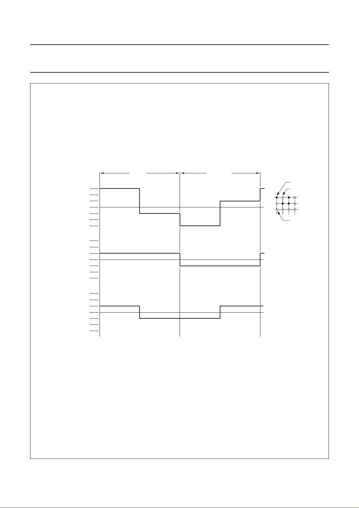
handbook, full pagewidth
ROW 17
ROW 18
ROW 1 to 16
COL 1
ON/OFF
COL 2
OFF
/ON
V
V
V
V
V
LCD
2/3
1/3
V
SS
LCD
2/3
1/3
V
SS
LCD
2/3
1/3
V
SS
LCD
2/3
1/3
V
SS
LCD
2/3
1/3
V
SS
frame n + 1 frame n
only icons are
driven (MUX 1 : 2)
V
LCD
V
2/3
1/3
V
SS
LCD
2/3
1/3
V
SS
COL 3
COL 4
ON/ON
OFF/OFF
Fig.14 MUX 1 : 2 LCD waveforms; icon mode.
2003 Jan 30 19
MGE997
Philips Semiconductors Product specification
LCD controllers/drivers PCF2119X
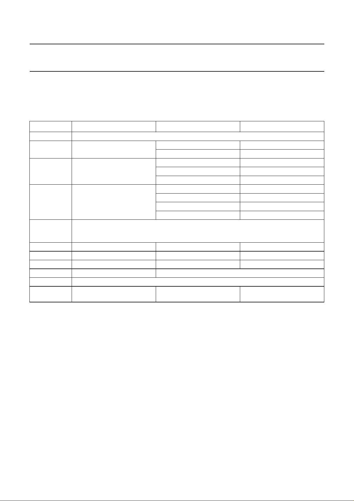
handbook, full pagewidth
state 1
COL 1 -
ROW 17
state 2
COL 2 -
ROW 17
state 3
COL 1 -
ROW 1 to 16
V
2/3 V
1/3 V
−1/3 V
−2/3 V
−V
2/3 V
1/3 V
−1/3 V
−2/3 V
−V
2/3 V
1/3 V
−1/3 V
−2/3 V
−V
PIXEL
V
OP
OP
OP
OP
OP
OP
V
OP
OP
OP
OP
OP
OP
V
OP
OP
OP
OP
OP
OP
frame n + 1 frame n
state 1 (ON)
state 2 (OFF)
R17
0
R18
R1-16
state 3 (OFF)
0
0
MGE998
V
= 0.745V
ON(rms)
V
OFF(rms)
D
V
ON
------------V
OFF
= 0.333V
2.23==
OP
OP
Fig.15 MUX 1 : 2 LCD waveforms; icon mode.
2003 Jan 30 20
Philips Semiconductors Product specification
LCD controllers/drivers PCF2119X
7.17 Reset function
The PCF2119x must be reset externally when power is turned on. The reset executes a ‘clear display’, requiring
165 oscillator cycles. After the reset the chip has the state shown in Table 4.
Table 4 State after reset
STEP FUNCTION CONTROL BIT STATE CONDITION
1 clear display
2 entry mode set I/D = 1 +1 (increment)
S = 0 no shift
3 display control D = 0 display off
C = 0 cursor off
B = 0 cursor character blink off
4 function set DL = 1 8-bit interface
M = 0 1-line display
H = 0 normal instruction set
SL = 0 MUX 1 : 18 mode
5 default address pointer to DDRAM; the Busy Flag (BF) indicates the busy state (BF = 1) until
initialization ends; the busy state lasts 2 ms; the chip may also be initialized by software; see
Tables 18 and 19
6 icon control IM, IB = 00 icons/icon blink disabled
7 display/screen configuration L = 0; P = 0; Q = 0 default configurations
8V
9 set V
10 I
11 set HVgen stages S1 = 1, S0 = 0 HVgen set to 3 internal stages
temperature coefficient TC1 = 0; TC2 = 0 default temperature coefficient
LCD
LCD
2
C-bus interface reset
VA= 0; VB= 0 (V
generator off)
LCD
(4 voltage multipliers)
2003 Jan 30 21

Philips Semiconductors Product specification
LCD controllers/drivers PCF2119X
8 INSTRUCTIONS
Onlytwo PCF2119x registers, the Instruction Register (IR)
and the Data Register (DR) can be directly controlled by
the MPU. Before internal operation, control information is
storedtemporarily in these registers, to allow interfacing to
various types of MPUs which operate at different speeds
or to allow interface to peripheral control ICs. The
PCF2119x operation is controlled by the instructions
shown in Table 6 together with their execution time.
Details are explained in subsequent sections.
Instructions are of 4 types, those that:
1. Designate PCF2119x functions such as display
format, data length, etc.
2. Set internal RAM addresses
3. Perform data transfer with internal RAM
4. Others.
2
Table 5 Instruction set for I
CONTROL BYTE COMMAND BYTE I
CoRS000000DB7DB6DB5DB4DB3DB2DB1DB0note 1
Note
1. R/
W is set together with the slave address.
C-bus commands
In normal use, category 3 instructions are used most
frequently. However, automatic incrementing by 1
(or decrementing by 1) of internal RAM addresses after
each data write lessens the MPU program load. The
display shift in particular can be performed concurrently
with display data write, enabling the designer to develop
systems in minimum time with maximum programming
efficiency.
During internal operation, no instructions other than the
‘read busy flag’ and ‘read address’ instructions will be
executed.Becausethebusyflagissettoalogic 1whilean
instructionisbeing executed, check to ensure it is a logic 0
before sending the next instruction or wait for the
maximum instruction execution time, as given in Table 6.
An instruction sent while the busy flag is logic 1 will not be
executed.
2
C-BUS COMMANDS
2003 Jan 30 22

Philips Semiconductors Product specification
LCD controllers/drivers PCF2119X
CLOCK
REQUIRED
CYCLES
3
0
display lines (M); single line/MUX 1 : 9 (SL),
extended instruction set control (H)
reads the Busy Flag (BF) indicating internal
operating is being performed and reads address
counter contents
3
165
in address counter
returns shifted display to original position;
DDRAM contents remain unchanged
3
display; these operations are performed during
3
data write and read
blink of cursor position character (B); D = 0
(display off) puts chip into the power-down mode
3
3
sets CGRAM address; bit 6 is to be set by the
command ‘set DDRAM address’; look at the
DDRAM contents
description of the commands
sets DDRAM address 3
This text is here in white to force landscape pages to be rotated correctly when browsing through the pdf in the Acrobat reader.This text is here in
_white to force landscape pages to be rotated correctly when browsing through the pdf in the Acrobat reader.This text is here inThis text is here in
white to force landscape pages to be rotated correctly when browsing through the pdf in the Acrobat reader. white to force landscape pages to be ...
Table 6 Instruction set with parallel bus commands; note 1
2003 Jan 30 23
INSTRUCTION RS R/W DB7 DB6 DB5 DB4 DB3 DB2 DB1 DB0 DESCRIPTION
H=0or1
NOP 0000000000no operation 3
Function set 00001DL0MSLHsets interface Data Length (DL) and number of
C
0 1 BF A
Read busy flag
and address
counter
CG
DD
000001S/CR/L00moves cursor and shifts display without changing
0001 A
Read data 1 1 read data reads data from CGRAM or DDRAM 3
Write data 1 0 write data writes data from CGRAM or DDRAM 3
H=0
Clear display 0000000001clears entire display and sets DDRAM address 0
Return home 0000000010sets DDRAM address 0 in address counter; also
Entry mode set 00000001I/DSsets cursor move direction and specifies shift of
Display control 0000001DCBsets entire display on/off (D), cursor on/off (C) and
Cursor/display
shift
Set CGRAM
address
001 A
Set DDRAM
address
H=1
Reserved 0000000001do not use −

Philips Semiconductors Product specification
LCD controllers/drivers PCF2119X
−
CLOCK
CYCLES
REQUIRED
(V) 3
B
or V
A
in register V
LCD
allowed)
This text is here in white to force landscape pages to be rotated correctly when browsing through the pdf in the Acrobat reader.This text is here in
_white to force landscape pages to be rotated correctly when browsing through the pdf in the Acrobat reader.This text is here inThis text is here in
white to force landscape pages to be rotated correctly when browsing through the pdf in the Acrobat reader. white to force landscape pages to be ...
INSTRUCTION RS R/W DB7 DB6 DB5 DB4 DB3 DB2 DB1 DB0 DESCRIPTION
2003 Jan 30 24
000000001Lset screen configuration 3
Screen
configuration
00000001PQset display configuration 3
Display
configuration
00000100TC1TC2set temperature coefficient (TCx) 3
Icon control 0000001IMIB0set icon mode (IM), icon blink (IB) 3
Temperature
control
0 0 1 V voltage store V
00010000S1S0set internal HVgen stages (S1 = 1 and S0 = 1 not
LCD
Set HVgen
stages
Set V
Note
1. X = don’t care.

Philips Semiconductors Product specification
LCD controllers/drivers PCF2119X
Table 7 Explanations of symbols used in Table 6
BIT
STATE
LOGIC 0 LOGIC 1
I/D decrement increment
S display freeze display shift
D display off display on
C cursor off cursor on
B cursor character blink off: character at cursor
position does not blink
cursor character blink on: character at cursor
position blinks
S/C cursor move display shift
R/L left shift right shift
DL 4 bits 8 bits
H use basic instruction set use extended instruction set
L (no impact, if
M = 1 or SL = 1)
P column data: left to right (as in PCF2116);
left/right screen: standard connection (as in
PCF2114)
1st 16 characters of 32: columns are from
1to80
2nd 16 characters of 32: columns are from
1to80
column data is displayed from 1 to 80
left/right screen: mirrored connection (as in
PCF2116)
1st 16 characters of 32: columns are from
1to80
2nd 16 characters of 32: columns are from
80 to 1
column data: right to left; column data is
displayed from 80 to 1
Q row data top to bottom (as in PCF2116): row data bottom to top:
rowdata is displayed from 1 to 16andicon row
data in 17 and 18
in single line mode (SL = 1) row data is
displayed from 1 to 8 and icon row data in 17
rowdata is displayed from 16 to 1andicon row
data in 18 and 17
in single line mode (SL = 1) row data is
displayed from 8 to 1 and icon row data in 17
IM character mode; full display icon mode; only icons displayed
IB icon blink disabled icon blink enabled
DM direct mode disable direct mode enable
V set V
M (no impact, if
1-line by 32 display 2-line by 16 display
A
set V
B
SL = 1)
SL MUX 1 : 18 (1 × 32 or 2 × 16 character display) MUX1:9 (1×16 character display)
C
0
last control byte; see Table 5 another control byte follows after data/command
Table 8 Explanation of TC1 and TC2 used in Table 6
TC1 TC2 DESCRIPTION
00V
10V
01V
11V
temperature coefficient 0
LCD
temperature coefficient 1
LCD
temperature coefficient 2
LCD
temperature coefficient 3
LCD
Note
1. For values of the temperature coefficients, see Chapter 13
2003 Jan 30 25
(1)

Philips Semiconductors Product specification
LCD controllers/drivers PCF2119X
Table 9 Explanation of S1 and S0 used in Table 6
S1 S0 DESCRIPTION
0 0 set internal HVgen stages to 1 (2 × voltages multiplier)
o 1 set internal HVgen stages to 2 (3 × voltages multiplier)
1 0 set internal HVgen stages to 3 (4 × voltages multiplier)
1 1 do not use
RS
R/W
E
DB7
DB6
DB5
DB4
IR7 IR3 BF AC3 DR7 DR3
IR6 IR2 AC6 AC2 DR6 DR2
IR5 IR1 AC5 AC1 DR5 DR1
IR4 IR0 AC4 AC0 DR4 DR0
instruction
write
busy flag and
address counter read
data register
read
Fig.16 4-bit transfer example.
MGA804
2003 Jan 30 26

Philips Semiconductors Product specification
LCD controllers/drivers PCF2119X
RS
R/W
E
internal
DB7
IR7, IR3: instruction 7th, 3rd bit.
AC3: address counter 3rd bit.
D7, D3: data 7th, 3rd bit.
RS
R/W
internal operation
IR7 IR3 AC3 D7 D3
instruction
write
busy
busy flag
AC3
check
not
busy
busy flag
check
instruction
write
Fig.17 An example of 4-bit data transfer timing sequence.
MGA805
E
internal
DB7
data busy busy
instruction
write
internal operation
busy flag
check
Fig.18 Example of busy flag checking timing sequence.
2003 Jan 30 27
busy flag
check
not
busy
busy flag
check
data
instruction
write
MGA806

Philips Semiconductors Product specification
LCD controllers/drivers PCF2119X
8.1 Clear display
‘Clear display’ writes character code 20H into all DDRAM
addresses (the character pattern for character code 20H
must be a blank pattern), sets the DDRAM address
counter to logic 0 and returns the display to its original
position, if it was shifted. Thus, the display disappears and
the cursor or blink position goes to the left edge of the
display. Sets entry mode I/D = 1 (increment mode). S of
entry mode does not change.
The instruction ‘clear display’ requires extra execution
time. This may be allowed by checking the Busy Flag (BF)
or by waiting until the 165 clock cycles have elapsed. The
latter must be applied where no read-back options are
foreseen, as in some Chip-On-Glass (COG) applications.
8.2 Return home
‘Return home’ sets the DDRAM address counter to logic 0
and returns the display to its original position if it was
shifted. DDRAM contents do not change. The cursor or
blink position goes to the left of the first display line.
I/D and S of entry mode do not change.
8.3 Entry mode set
8.3.1 I/D
When I/D = 1 (0) the DDRAM or CGRAM address
increments (decrements) by 1 when data is written into or
read from the DDRAM or CGRAM. The cursor or blink
position moves to the right when incremented and to the
left when decremented. The cursor underline and cursor
character blink are inhibited when the CGRAM is
accessed.
When the display is off (D = 0) the chip is in partial
power-down mode:
• The LCD outputs are connected to V
SS
• The LCD generator and bias generator are turned off.
Three oscillator cycles are required after sending the
‘display off’ instruction to ensure all outputs are at VSS,
afterwards OSC can be stopped. If the oscillator is running
duringpartial power-down mode (‘display off’) the chip can
still execute instructions. Even lower current consumption
is obtained by inhibiting the oscillator (OSC = VSS).
To ensure IDD<1 µA, the parallel bus pads DB7 to DB0
should be connected to VDD; RS and R/W to VDD or left
open-circuit and PD to VDD. Recovery from power-down
mode: PD back to logic 0, if necessary OSC back to V
DD
and send a ‘display control’ instruction with D = 1.
8.4.2 C
The cursor is displayed when C = 1 and inhibited when
C = 0. Even if the cursor disappears, the display functions
I/D, etc. remain in operation during display data write. The
cursor is displayed using 5 dots in the 8th line (see Fig.5).
8.4.3 B
The character indicated by the cursor blinks when B = 1.
The cursor character blink is displayed by switching
between display characters and all dots on with a period of
f
approximately 1 second, with
f
blink
=
OSC
---------------- 52224
Thecursor underline and the cursor character blink can be
set to display simultaneously.
8.3.2 S
When S = 1, the entire display shifts either to the right
(I/D = 0)ortothe left (I/D = 1) during a DDRAM write. Thus
it appears as if the cursor stands still and the display
moves. The display does not shift when reading from the
DDRAM, or when writing to or reading from the CGRAM.
When S = 0, the display does not shift.
8.4 Display control (and partial power-down mode)
8.4.1 D
The display is on when D = 1 and off when D = 0. Display
data in the DDRAM is not affected and can be displayed
immediately by setting D to a logic 1.
2003 Jan 30 28
8.5 Cursor or display shift
‘Cursor/display shift’ moves the cursor position or the
display to the right or left without writing or reading display
data. This function is used to correct a character or move
the cursor through the display. In 2-line displays, the
cursor moves to the next line when it passes the last
position (40) of the line.
Whenthe displayed data is shifted repeatedly all lines shift
at the same time; displayed characters do not shift into the
next line.
The Address Counter (AC) content does not change if the
only action performed is shift display, but increments or
decrements with the ‘cursor shift’.

Philips Semiconductors Product specification
LCD controllers/drivers PCF2119X
8.6 Function set
8.6.1 DL (PARALLEL MODE ONLY)
Sets interface data width. Data is sent or received in bytes
(DB7 to DB0) when DL = 1 or in two nibbles (DB7 to DB4)
when DL = 0. When 4-bit width is selected, data is
transmitted in two cycles using the parallel bus. In a 4-bit
applicationDB3 to DB0 should beleftopen-circuit (internal
pull-ups). Hence in the first ‘function set’ instruction after
power-on, M, SL and H are set to logic 1. A second
‘function set’ must then be sent (2 nibbles) to set M,
SL and H to their required values.
‘Function set’ from the I2C-bus interface sets the DL bit to
logic 1.
8.6.2 M
Selects either 1-line by 32 display (M = 0) or 2-line by
16 display (M = 1).
8.6.3 SL
Selects MUX 1 : 9, 1-line by 16 display (independent of
M and L). Only rows 1 to 8 and 17 are to be used.All other
rows must be left open-circuit. The DDRAM map is the
same as in the 2-line by 16 display mode, however, the
second line is not displayable.
8.6.4 H
8.8 Set DDRAM address
‘Set DDRAM address’ sets the DDRAM address ADD into
the address counter (binary A6 to A0). Data can then be
written to or read from the DDRAM.
8.9 Read busy flag and read address
‘Read busy flag’ and ‘read address’ read the Busy Flag
(BF) and Address Counter (AC). BF = 1 indicates that an
internal operation is in progress. The next instruction will
not be executed until BF = 0. It is recommended that the
BF status is checked before the next write operation is
executed.
At the same time, the value of the address counter
expressed in binary A6 to A0 is read out. The address
counter is used by both CGRAM and DDRAM, and its
value is determined by the previous instruction.
8.10 Write data to CGRAM or DDRAM
‘Write data’ writes binary 8-bit data D7 to D0 to the
CGRAM or the DDRAM.
Whether the CGRAM or DDRAM is to be written into is
determined by the previous ‘set CGRAM address’ or ‘set
DDRAM address’ command. After writing, the address
automatically increments or decrements by 1, in
accordance with the entry mode. Only bits D4 to D0 of
CGRAM data are valid, bits D7 to D5 are ‘don’t care’.
When H = 0 the chip can be programmed via the standard
11 instruction codes used in the PCF2116 and other LCD
controllers.
When H = 1 the extended range of instructions will be
used. These are mainly for controlling the display
configuration and the icons.
8.7 Set CGRAM address
‘Set CGRAM address’ sets bits 5 to 0 of the CGRAM
address ACG into the address counter (binary A5 to A0).
Data can then be written to or read from the CGRAM.
Attention: the CGRAM address uses the same address
register as the DDRAM address and consists of 7 bits
(binary A6 to A0). With the ‘set CGRAM address’
command, only bits 5 to 0 are set. Bit 6 can be set using
the ‘set DDRAM address’ command first, or by using the
auto-incrementfeature during CGRAM write. All bits 6 to 0
can be read using the ‘read busy flag’ and ‘read address’
command.
When writing to the lower part of the CGRAM, ensure that
bit 6 of the address is not set (e.g. by an earlier DDRAM
write or read action).
8.11 Read data from CGRAM or DDRAM
‘Read data’ reads binary 8-bit data D7 to D0 from the
CGRAM or DDRAM.
The most recent ‘set address’ command determines
whether the CGRAM or DDRAM is to be read.
The ‘read data’ instruction gates the content of the Data
Register (DR) to the bus while E is HIGH. After E goes
LOWagain,internaloperation increments (or decrements)
the AC and stores RAM data corresponding to the new AC
into the DR.
There are only three instructions that update the data
register:
• ‘set CGRAM address’
• ‘set DDRAM address’
• ‘read data’ from CGRAM or DDRAM.
Other instructions (e.g. ‘write data’, ‘cursor/display shift’,
‘clear display’ and ‘return home’) do not modify the data
register content.
2003 Jan 30 29

Philips Semiconductors Product specification
LCD controllers/drivers PCF2119X
9 EXTENDED FUNCTION SET INSTRUCTIONS AND
FEATURES
9.1 New instructions
H = 1, sets the chip into alternate instruction set mode.
9.4 IB
Icon blink control is independent of the cursor/character
blink function.
When IB = 0, icon blink is disabled. Icon data is stored in
CGRAM character 0 to 3 (4 × 8 × 5 = 160 bits for
9.2 Icon control
The PCF2119x can drive up to 160 icons. See Fig.19 for
CGRAM to icon mapping.
160 icons).
When IB = 1, icon blink is enabled. In this case each icon
is controlled by two bits. Blink consists of two half phases
(correspondingtothe cursor on and off phasescalledeven
9.3 IM
When IM = 0, the chip is in character mode. In the
character mode characters and icons are driven
(MUX 1 : 18). The V
V
voltage programmed in register VA.
LCD
generator, if used, produces the
LCD
When IM = 1, the chip is in icon mode. In the icon mode
only the icons are driven (MUX1:2)andtheV
generator, if used, produces the V
voltage as
LCD
LCD
voltage
programmed in register VB.
and odd phases hereafter).
Icon states for the even phase are stored in CGRAM
characters 0 to 3 (4 × 8 × 5 = 160 bits for 160 icons).
These bits also define the icon state when icon blink is not
used.
Icon states for the odd phase are stored in CGRAM
character4 to 7 (another 160 bits for the 160 icons). When
icon blink is disabled CGRAM characters 4 to 6 may be
used as normal CGRAM characters.
Table 10 Blink effect for icons and cursor character blink
PARAMETER EVEN PHASE ODD PHASE
Cursor character blink block (all on) normal (display character)
Icons state 1: CGRAM character 0 to 2 state 2: CGRAM character 4 to 6
2003 Jan 30 30

Philips Semiconductors Product specification
LCD controllers/drivers PCF2119X
handbook, full pagewidth
handbook, full pagewidth
icon no. phase ROW/COL character codes CGRAM address CGRAM data
1-5 even 17/1-5 0 0 0 0 0 0 0 0 0 0 0 0 0 0 0 1 0 1 0 1
6-10 even 17/6-10 0 0 0 0 0 0 0 0 0 0 0 0 0 0 1 0 1 0 1 0
11-15 even 17/11-15 0 0 0 0 0 0 0 0 0 0 0 0 0 1 0 0 1 1 1 0
display:
ROW 17 –
ROW 18 –
COL 1 to 5
12345
81 82 83 84 85
block of 5 columns
7 6 5 4 3 2 1 0
MSB LSB LSB
COL 6 to 10
678910
86 87 88 89 90
6 5 4 3 2 1 0 4 3 2 1 0
MSB MSBLSB
COL 76 to 80
76 77 78 79 80
156 157 158 159 160
MGL249
icon view
76-80 even 17/76-80 0 0 0 0 0 0 0 1 0 0 0 1 1 1 1 1 1 1 1 1
81-85 even 18/1-5 0 0 0 0 0 0 1 0 0 0 1 0 0 0 0 1 1 0 0 0
156-160 even 18/76-80 0 0 0 0 0 0 1 1 0 0 1 1 1 1 1 1 1 1 0 1
1-5 odd (blink) 17/1-5 0 0 0 0 0 1 0 0 0 1 0 0 0 0 0 0 0 0 0 0
156-160 odd (blink) 18/76-80 0 0 0 0 0 1 1 1
CGRAM data bit = logic 1 turns the icon on, data bit = logic 0 turns the icon off.
Data in character codes 0 to 3 define the icon state when icon blink is disabled or during the even phase when icon blink is enabled.
Data in character codes 4 to 7 define the icon state during the odd phase when icon blink is enabled (not used for icons when icon blink is disabled).
0 1 1 1 1 1 1 0 0 1 1 0
MGK999
Fig.19 CGRAM to icon mapping.
2003 Jan 30 31

Philips Semiconductors Product specification
LCD controllers/drivers PCF2119X
9.5 Normal/icon mode operation
IM CONDITION V
0 character mode generates V
1 icon mode generates V
LCD
A
B
9.6 Direct mode
When DM = 0, the chip is not in direct mode. Either the
internal voltage generator or an external voltage may be
used to achieve the necessary V
LCD
value.
When DM = 1, the chip is in direct mode. The internal
voltage generator is turned off and the V
directly connected to the HVgen supply voltage V
output is
LCD
DD2
.
The direct mode can be used to reduce the current
consumption when the required V
close to the V
supply voltage. This can be the case in
DD2
output voltage is
LCD
icon mode or in Mux 1 : 9 (depending on LCD liquid
properties).
9.7 Voltage multiplier control
S[1:0]
A software configurable voltage multiplier is incorporated
and can be set via ‘Set HVgen stages’ command.
The voltage multiplier control can be used to reduce
current consumption by disconnecting internal voltage
multiplier stages (depending on the required V
LCD
output
voltage).
9.11 Set V
TheV
registers hold V
icon mode respectively (VAand VB). The generated V
LCD
valueisprogrammed by instruction. Two on-chip
LCD
values for the character mode and the
LCD
LCD
value is independent of VDD, allowing battery operation of
the chip.
V
programming:
LCD
1. Send ‘function set’ instruction with H = 1
2. Send ‘set V
a) DB7, DB6 = 10: DB5 to DB0 are V
’ instruction to write to voltage register:
LCD
of character
LCD
mode (VA)
b) DB7,DB6 = 11: DB5 to DB0 are V
)
(V
B
c) DB5 to DB0 = 000000 switches V
oficon mode
LCD
generator off
LCD
(when selected)
d) During ‘display off’ and power-down the V
LCD
generator is also disabled.
3. Send ‘function set’ instruction with H = 0 to resume
normal programming.
9.12 Reducing current consumption
Reducing current consumption can be achieved by one of
the options given in Table 11.
When V
lies outside the VDD range and must be
LCD
generated, it is usually more efficient to use the on-chip
generator than an external regulator.
9.8 Screen configuration
L: default is L = 0.
L = 0: the two halves of a split screen are connected in a
standard way i.e. column 1/81, 2/82 to 80/160.
L = 1: the two halves of a split screen are connected in a
mirrored way i.e. column 1/160, 2/159 to 80/81. This
allows single layer PCB or glass layout.
9.9 Display configuration
P, Q: default is P, Q = 0.
P = 1: mirrors the column data.
Q = 1: mirrors the row data.
9.10 TC1 and TC2
Default is TC1 and TC2 = 0. This selects the default
temperature coefficient for the internally generated V
LCD
.
TC1 and TC2 = 10, 01 and 11 selects alternative
temperature coefficients 1, 2 and 3 respectively.
2003 Jan 30 32
Table 11 Reducing current consumption
ORIGINAL MODE ALTERNATIVE MODE
Character mode icon mode (control bit IM)
Display on display off (control bit D)
HV generator operating direct mode
Any mode power-down (PD pad)
Table 12 Use of the VA and VB registers
MODE V
Normal operation V
character
LCD
A
V
V
icon mode
LCD
B
mode

Philips Semiconductors Product specification
LCD controllers/drivers PCF2119X
10 INTERFACES TO MPU
10.1 Parallel interface
ThePCF2119x can send dataineithertwo 4-bit operations
or one 8-bit operation and can thus interface to 4-bit or
8-bit microcontrollers.
In 8-bit mode data is transferred as 8-bit bytes using the
8 data lines DB7 to DB0. Three further control lines
E, RS and R/W are required; see Section 6.1.
In 4-bit mode data is transferred in two cycles of 4 bits
each using pads DB7 to DB4 for the transaction. The
higher order bits (corresponding to DB7 to DB4 in 8-bit
mode) are sent in the first cycle and the lower order bits
(DB3 to DB0 in 8-bit mode) in the second. Data transfer is
complete after two 4-bit data transfers. It should be noted
that two cycles are also required for the busy flag check.
4-bitoperationisselected by instruction, see Figs 16 to 18
for examples of bus protocol.
In 4-bit mode, pads DB3 to DB0 must be left open-circuit.
They are pulled up to VDD internally.
2
10.2 I
C-bus interface
The I2C-bus is for bidirectional, two-line communication
between different ICs or modules. The two lines are the
Serial Data line (SDA) and the Serial Clock Line (SCL).
Both lines must be connected to a positive supply via
pull-up resistors. Data transfer may be initiated only when
the bus is not busy.
Each byte of eight bits is followed by an acknowledge bit.
The acknowledge bit is a HIGH level signal put on the bus
by the transmitter during which time the master generates
anextraacknowledge related clock pulse. A slave receiver
which is addressed must generate an acknowledge after
the reception of each byte.
Also a master receiver must generate an acknowledge
after the reception of each byte that has been clocked out
of the slave transmitter.
The device that acknowledges must pull-down the SDA
line during the acknowledge clock pulse, so that the SDA
line is stable LOW during the HIGH period of the
acknowledge related clock pulse (set-up and hold times
must be taken into consideration).
A master receiver must signal an end of data to the
transmitter by not generating an acknowledge on the last
byte that has been clocked out of the slave. In this event
thetransmittermustleavethedatalineHIGH to enable the
master to generate a STOP condition.
10.2.1 I2C-BUS PROTOCOL
Before any data is transmitted on the I2C-bus, the device
whichshouldrespondis addressed first. The addressing is
always carried out with the first byte transmitted after the
START procedure. The I2C-bus configuration for the
different PCF2119x read and write cycles is shown in
Figs 24 to 26. The slow down feature of the I2C-bus
protocol (receiver holds SCL LOW during internal
operations) is not used in the PCF2119x.
10.2.2 DEFINITIONS
• Transmitter: the device which sends the data to the bus
• Receiver: the device which receives the data from the
bus
• Master: the device which initiates a transfer, generates
clock signals and terminates a transfer
• Slave: the device addressed by a master
• Multi-master: more than one master can attempt to
control the bus at the same time without corrupting the
message
• Arbitration: procedure to ensure that, if more than one
master simultaneously tries to control the bus, only one
is allowed to do so and the message is not corrupted
• Synchronization: procedure to synchronize the clock
signals of two or more devices.
SLAVE
TRANSMITTER/
RECEIVER
SDA
SCL
MASTER
TRANSMITTER/
RECEIVER
SLAVE
RECEIVER
Fig.20 System configuration.
2003 Jan 30 33
MASTER
TRANSMITTER
MASTER
TRANSMITTER/
RECEIVER
MGA807

Philips Semiconductors Product specification
LCD controllers/drivers PCF2119X
handbook, full pagewidth
SDA
SCL
handbook, full pagewidth
SDA
SCL
S
START condition
Fig.22 Definition of START and STOP conditions.
data line
stable;
data valid
change
of data
allowed
Fig.21 Bit transfer.
MBC621
P
STOP condition
SDA
SCL
MBC622
handbook, full pagewidth
DATA OUTPUT
BY TRANSMITTER
DATA OUTPUT
BY RECEIVER
SCL FROM
MASTER
S
START
condition
Fig.23 Acknowledgement on the I2C-bus.
2003 Jan 30 34
not acknowledge
acknowledge
acknowledgement
9821
clock pulse for
MBC602

Philips Semiconductors Product specification
LCD controllers/drivers PCF2119X
MGK899
A
DATA BYTE
A
update
data pointer
handbook, full pagewidth
from PCF2119x
acknowledgement
S
1 byte n ≥ 0 bytes2n ≥ 0 bytes
CONTROL BYTE
0
A
DATA BYTE
A
CONTROL BYTE
RS RS
1
0A
0
A
Co
Co
R/W
Fig.24 Master transmits to slave receiver; write mode.
0
0
S
A
R/W
This text is here in white to force landscape pages to be rotated correctly when browsing through the pdf in the Acrobat reader.This text is here in
_white to force landscape pages to be rotated correctly when browsing through the pdf in the Acrobat reader.This text is here inThis text is here in
white to force landscape pages to be rotated correctly when browsing through the pdf in the Acrobat reader. white to force landscape pages to be ...
2003 Jan 30 35
011101
slave address
S P
PCF2119x
011101
slave address

Philips Semiconductors Product specification
LCD controllers/drivers PCF2119X
A
handbook, full pagewidth
(1)
DATA BYTE
A
1 byte n ≥ 0 bytes
CONTROL BYTE
0
A
DATA BYTE
A
Co
2n 0 bytes
P
DATA BYTE
1A DATA BYTE A 1
0
S
acknowledgement acknowledgement no acknowledgement
A
MGG003
update
data pointer
data pointer
n bytes last byte
Co update
R/W
This text is here in white to force landscape pages to be rotated correctly when browsing through the pdf in the Acrobat reader.This text is here in
_white to force landscape pages to be rotated correctly when browsing through the pdf in the Acrobat reader.This text is here inThis text is here in
white to force landscape pages to be rotated correctly when browsing through the pdf in the Acrobat reader. white to force landscape pages to be ...
2003 Jan 30 36
CONTROL BYTE
RS RS
1
A
0
S
acknowledgement
A
011101
S
0
Co
R/W
slave address
SLAVE
ADDRESS
S
Fig.25 Master reads after setting word address; writes word address, set RS; ‘read data’.
(1) Last data byte is a dummy byte (may be omitted).

Philips Semiconductors Product specification
LCD controllers/drivers PCF2119X
handbook, full pagewidth
Fig.26 Master reads slave immediately after first byte; read mode (RS previously defined).
handbook, full pagewidth
SDA
S
SLAVE
ADDRESS
acknowledgement
from PCF2113x
S
A
1A DATA BYTE A 1
0
R/W
Co update
acknowledgement
from master
DATA BYTE
n bytes last byte
data pointer
no acknowledgement
from master
P
update
data pointer
MGG004
SCL
SDA
MGA728
t
BUF
t
HD;STA
t
LOW
t
r
Fig.27 I2C-bus timing diagram.
2003 Jan 30 37
t
SU;STA
t
HD;DAT
t
HIGH
t
f
t
SU;DAT
t
SU;STO

Philips Semiconductors Product specification
LCD controllers/drivers PCF2119X
11 LIMITING VALUES
In accordance with the Absolute Maximum Rating System (IEC 60134).
SYMBOL PARAMETER MIN. MAX. UNIT
V
DD1
V
DD2
V
LCD
V
DD(I/O)
V
LCD(I/O)
I
I
I
O
I
, ISS and I
DD
P
tot
P
O
T
stg
, V
DD3
logic supply voltage −0.5 +6.5 V
high voltage generator supply voltage −0.5 +4.5 V
LCD supply voltage −0.5 +7.5 V
any VDD related input/output voltage −0.5 VDD+ 0.5 V
any V
related input/output voltage −0.5 V
LCD
LCD
DC input current −10 +10 mA
DC output current −10 +10 mA
LCDVDD1
DD2
DD3
SS1
SS2
or V
current −50 +50 mA
LCD
, V
, V
, V
, V
total power dissipation − 400 mW
power dissipation per output − 100 mW
storage temperature −65 +150 °C
+ 0.5 V
12 HANDLING
Inputs and outputs are protected against electrostatic discharge in normal handling. However, to be totally safe, it is
desirable to take normal precautions appropriate to handling MOS devices (see
“Handling MOS Devices”
).
2003 Jan 30 38

Philips Semiconductors Product specification
LCD controllers/drivers PCF2119X
13 DC CHARACTERISTICS
V
= 1.5 to 5.5 V; V
DD1
DD2=VDD3
specified.
SYMBOL PARAMETER CONDITIONS MIN. TYP. MAX. UNIT
Supplies
V
V
V
V
DD1
DD2
DD3
LCD
logic supply voltage 1.5 − 5.5 V
,
high voltage generator supply
voltage
LCD supply voltage 2.2 − 6.5 V
GROUND SUPPLY CURRENT (ISS); EXTERNAL V
I
SS1
I
SS3
I
SS4
I
SS5
ground supply current 1 − 70 120 µA
ground supply current 3 VDD=3V; V
ground supply current 4 icon mode; VDD=3V;
ground supply current 5 power-down mode;
GROUND SUPPLY CURRENT (ISS); INTERNAL V
I
SS6
I
SS8
I
SS9
ground supply current 6 − 190 400 µA
ground supply current 8 VDD=3V; V
ground supply current 9 icon mode; VDD= 2.5 V;
Logic
V
IL
V
IH
V
IL(osc)
LOW-level input voltage V
HIGH-level input voltage 0.7V
LOW-level input voltage
pad OSC
V
IH(osc)
I
OL(DB)
HIGH-level voltage pad OSC VDD=V
LOW-level output current pads
DB7 to DB0
I
OH(DB)
HIGH-level output current pads
DB7 to DB0
I
pu
I
L
pull-up current pads DB7 to DB0 VI=VSS, V
leakage current VI=V
= 2.2 to 4.0 V; VSS=0V;V
internal V
(V
DD2=VDD3<VLCD
; note 1
LCD
LCD
note 2
V
= 2.5 V; note 2
LCD
VDD=3V; V
DB7 to DB0,
RS and R/W = 1; OSC = 0;
PD = 1
; notes 1 and 3
LCD
note 2
V
= 2.5 V; note 2
LCD
VDD=V
DD(min)
DD(min)
VOL= 0.4 V; V
VOH=4V; V
DD(min)
DD1,2,3
= 2.2 to 6.5 V; T
LCD
generation
= −40 to +85 °C; unless otherwise
amb
2.2 − 4.0 V
)
LCD
=5V;
− 35 80 µA
− 25 45 µA
− 0.5 5 µA
= 2.5 V;
LCD
LCD
=5V;
− 135 400 µA
− 85 −µA
SS1
DD1
, V
DD(max)
, V
DD(max)
= 5 V 1.6 4 − mA
DD1
=5V −1 −8 − mA
DD1
, V
DD(max)
or V
SS1,2
V
SS1
V
− 0.1 − V
DD1
0.04 0.15 1 µA
−1 − +1 µA
− 0.3V
− V
− V
DD1
DD1
DD1
DD1
− 1.2 V
V
V
V
2003 Jan 30 39

Philips Semiconductors Product specification
LCD controllers/drivers PCF2119X
SYMBOL PARAMETER CONDITIONS MIN. TYP. MAX. UNIT
I2C-bus
SDA AND SCL
V
IL2
V
IH2
I
LI
C
i
I
OL(SDA)
LOW-level input voltage 0 − 0.3V
HIGH-level input voltage 0.7V
input leakage current VI=VDDor V
SS
−1 − +1 µA
DD
− 5.5 V
DD
input capacitance − 5 − pF
LOW-level output current SDA VOL= 0.4 V; VDD>2V 3 −− mA
V
= 0.2VDD; VDD<2V 2 −− mA
OL
LCD outputs
R
O(ROW)
row output resistance pads
note 4 − 10 30 kΩ
R1 to R18
R
O(COL)
column output resistance pads
note 4 − 15 40 kΩ
C1 to C80
V
bias(tol)
bias tolerance pads R1 to R18
note 5 − 20 130 mV
and C1 to C80
V
LCD(tol)
TC0 V
TC1 V
TC2 V
TC3 V
V
tolerance T
LCD
temperature coefficient 0 −−0.16 − %/K
LCD
temperature coefficient 1 −−0.18 − %/K
LCD
temperature coefficient 2 −−0.21 − %/K
LCD
temperature coefficient 3 −−0.24 − %/K
LCD
=25°C; note 3
amb
V
<3V −−160 mV
LCD
<4V −−200 mV
V
LCD
V
<5V −−260 mV
LCD
V
<6V −−340 mV
LCD
Notes
1. LCD outputs are open-circuit; inputs at VDDor VSS; bus inactive.
2. T
3. LCD outputs are open-circuit; HV generator is on; load current I
amb
=25°C; f
= 200 kHz.
OSC
LCD
=5µA.
4. Resistance of output terminals (R1 to R18 and C1 to C80) with a load current of 10 µA; outputs measured one at a
time; external V
5. LCD outputs open-circuit; external V
LCD
; V
LCD
= 3 V; V
DD1=VDD2=VDD3
.
LCD
=3V.
V
2003 Jan 30 40

Philips Semiconductors Product specification
LCD controllers/drivers PCF2119X
14 AC CHARACTERISTICS
V
= 1.5 to 5.5 V; V
DD1
DD2=VDD3
specified.
SYMBOL PARAMETER CONDITIONS MIN. TYP. MAX. UNIT
f
FR
f
OSC
LCD frame frequency (internal clock) VDD= 5.0 V 45 95 147 Hz
oscillator frequency (not available at any
pad)
f
OSC(ext)
t
OSCST
external clock frequency 140 − 450 kHz
oscillator start-up time after power-down note 1 − 200 300 µs
Bus timing characteristics: parallel interface; note 2
WRITE OPERATION (WRITING DATA FROM MPU TO PCF2119X)
T
cy(en)
t
W(en)
t
su(A)
t
h(A)
t
su(D)
t
h(D)
enable cycle time 500 −−ns
enable pulse width 220 −−ns
address set-up time 50 −−ns
address hold time 25 −−ns
data set-up time 60 −−ns
data hold time 25 −−ns
READ OPERATION (READING DATA FROM PCF2119XTOMPU)
T
cy(en)
t
W(en)
t
su(A)
t
h(A)
t
d(D)
t
h(D)
enable cycle time 500 −−ns
enable pulse width 220 −−ns
address set-up time 50 −−ns
address hold time 25 −−ns
data delay time V
data hold time 20 − 100 ns
Timing characteristics: I
f
SCL
t
LOW
t
HIGH
t
SU;DAT
t
HD;DAT
t
r
t
f
C
B
t
SU;STA
SCL clock frequency −−400 kHz
SCL clock low period 1.3 −−µs
SCL clock high period 0.6 −−µs
data set-up time 100 −−ns
data hold time 0 −−ns
SCL, SDA rise time notes 1 and 3 15 + 0.1CB− 300 ns
SCL, SDA fall time notes 1 and 3 15 + 0.1CB− 300 ns
capacitive bus line load −−400 pF
set-up time for a repeated START
condition
t
HD;STA
t
SU;STO
t
SW
t
BUF
START condition hold time 0.6 −−µs
set-up time for STOP condition 0.6 −−µs
tolerable spike width on bus −−50 ns
bus free time between STOP and START
condition
= 2.2 to 4.0 V; VSS=0V;V
2
C-bus interface; note 2
= 2.2 to 6.5 V; T
LCD
= −40 to +85 °C; unless otherwise
amb
140 250 450 kHz
> 2.2 V −−150 ns
DD1
> 1.5 V −−250 ns
V
DD1
0.6 −−µs
1.3 −−µs
2003 Jan 30 41

Philips Semiconductors Product specification
LCD controllers/drivers PCF2119X
Notes
1. Tested on a sample basis.
2. All timing values are valid within the operating supply voltage and ambient temperature range and are referenced to
VIL and VIH with an input voltage swing of VSSto VDD.
3. CB= total capacitance of one bus line in pF.
15 TIMING CHARACTERISTICS
handbook, full pagewidth
handbook, full pagewidth
RS
R/W
DB0 to DB7
V
IH1
V
IL1
t
su(A)
V
IL1
t
W(en)
V
E
IH1
V
IL1
V
V
V
IH1
V
t
su(D)
IH1
IL1
IL1
valid data
V
IH1
V
IL1
T
cy(en)
t
t
h(A)
h(A)
V
t
h(D)
IL1
V
IL1
V
IH1
V
IL1
MBK474
Fig.28 Parallel bus write operation sequence; writing data from MPU to PCF2119x.
RS
R/W
V
V
V
IH1
IL1
t
su(A)
IH1
V
IH1
V
IL1
t
h(A)
V
IH1
t
W(en)
V
IH1
t
DB0 to DB7
E
V
IL1
Fig.29 Parallel bus read operation sequence; reading data from PCF2119x to MPU.
2003 Jan 30 42
V
d(D)
V
OH1
V
OL1
IH1
T
cy(en)
t
h(A)
V
IL1
t
h(D)
V
OH1
V
OL1
V
IL1
MBK475

Philips Semiconductors Product specification
LCD controllers/drivers PCF2119X
16 APPLICATION INFORMATION
16.1 General information
The required minimum value for the external capacitors in
an application with the PCF2119x are as follows: C
V
and V
LCD
V
= 470 nF. Higher capacitor values are
SS1,2
= 100 nF (min.), and for V
SS1,2
DD1,2,3
ext
and
for
recommended for ripple rejection.
For COG applications the recommended ITO track
resistance is to be minimized for the I/O and supply
connections. Optimized values for these are below 50 Ω
for the supply and below 100 Ω for the I/O connections.
handbook, full pagewidth
P21
P80CL51
RSP20
R/W
EP22
PCF2119x
DB7 to DB0P17 to P10
8
Higher track resistance reduces performance and
increases current consumption.
To avoid accidental triggering of power-on reset
(especially in COG applications), the supplies must be
adequately decoupled. Depending on power supply
quality, V
may have to be raised above the specified
DD1
minimum value.
When external V
open-circuit to avoid any stray current, and V
connected to V
R17, R18
R1 to R16
16
C1 to C80
is supplied, V
LCD
LCDSENSE
2
2 × 16 CHARACTER
LCD DISPLAY
PLUS 160 ICONS
80
.
LCD2
MGK895
should be left
must be
LCD1
Fig.30 Direct connection to 8-bit MPU; 8-bit bus.
handbook, full pagewidth
P11
P80CL51
RSP10
R/W
EP12
PCF2119x
DB7 to DB4P17 to P14
4
Fig.31 Direct connection to 8-bit MPU; 4-bit bus.
2003 Jan 30 43
R17, R18
R1 to R16
16
C1 to C80
2
2 × 16 CHARACTER
LCD DISPLAY
PLUS 160 ICONS
80
MGK896

Philips Semiconductors Product specification
LCD controllers/drivers PCF2119X
handbook, full pagewidth
handbook, full pagewidth
OSC
V
DD
100
nF
V
SS
100
nF
V
V
V
DD
LCD
SS
8
PCF2119x
RSDB7 to DB0 E
R17, R18
R1 to R16
16
C1 to C80
R/W
2
2 × 16 CHARACTER
LCD DISPLAY
PLUS 160 ICONS
80
MGK897
Fig.32 Typical application using parallel interface.
V
V
DD
DD
OSC
V
DD
100
nF
V
SS
V
V
100
nF
V
DD
PCF2119x
LCD
SS
SCL SDA
V
DD
DB3/SAO
R17, R18
R1 to R16
16
C1 to C80
2
2 × 16 CHARACTER
LCD DISPLAY
PLUS 160 ICONS
80
V
SS
DB3/SAO
OSC
SCL SDA
V
DD
100
nF
V
SS
MASTER TRANSMITTER
PCF84C81A; P80CL410
100
nF
V
DD
PCF2119x
V
LCD
V
SS
SCL SDA
Fig.33 Application using I2C-bus interface.
2003 Jan 30 44
R17, R18
R1 to R16
16
C1 to C80
MGK898
2
1 × 32 CHARACTER
LCD DISPLAY
PLUS 160 ICONS
80

Philips Semiconductors Product specification
LCD controllers/drivers PCF2119X
16.2 Charge pump characteristics
Typical graphs of the total power consumption of the
PCF2119x using the internal charge pump are illustrated
in Figs.34 to 36.
The graphs were obtained under the following conditions:
• T
• V
=25°C
amb
DD1=VDD2=VDD3
= 2.2 V (min.), 2.7 V (typ.) and 4 V
(max.)
• Normal mode
• f
= internal oscillator
osc
• Mux 1 : 18
• Typical current load for I
handbook, full pagewidth
I
DD
(µA)
400
350
LCD
=10µA.
For each multiplication factor there is a separate line. The
line ends where it is not possible to get a higher voltage
under its conditions (a higher multiplication factor is
needed to get higher voltages).
Connecting different displays may result in different
current consumption. This affects the efficiency and the
optimum multiplication factor to be used to generate a
certain output voltage.
MGW573
300
250
200
150
100
50
0
0
(1) 2 × multiplication factor.
(2) 3 × multiplication factor.
(3) 4 × multiplication factor.
(2)
(3)
(1)
2.75 3.5 4.25 5 5.75 6.5 7.25
Vop (V)
Fig.34 Typical charge pump characteristics for VDD= 2.2 V.
2003 Jan 30 45

Philips Semiconductors Product specification
LCD controllers/drivers PCF2119X
handbook, full pagewidth
(1) 2 × multiplication factor.
(2) 3 × multiplication factor.
(3) 4 × multiplication factor.
I
DD
(µA)
300
250
200
150
100
50
0
0
2.75 3.5 4.25 5 5.75 6.5 7.25
(1)
Fig.35 Typical charge pump characteristics for VDD= 2.7 V.
MGW574
(3)
(2)
Vop (V)
handbook, full pagewidth
(1) 2 × multiplication factor.
(2) 3 × multiplication factor.
(3) 4 × multiplication factor.
I
DD
(µA)
250
(3)
200
(2)
150
100
50
0
0
2.75 3.5 4.25 5 5.75 6.5 7.25
(1)
Fig.36 Typical charge pump characteristics for VDD=4V.
MGW575
Vop (V)
2003 Jan 30 46

Philips Semiconductors Product specification
LCD controllers/drivers PCF2119X
16.3 8-bit operation, 1-line display using external
reset
Table 14 shows an example of a 1-line display in 8-bit
operation. The PCF2119x functions must be set by the
‘functionset’ instruction prior to display. Since the DDRAM
can store data for 80 characters, the RAM can be used for
advertising displays when combined with display shift
operation. Since the display shift operation changes
display position only and the DDRAM contents remain
unchanged, display data entered first can be displayed
when the ‘return home’ operation is performed.
16.4 4-bit operation, 1-line display using external
reset
The program must set functions prior to a 4-bit operation,
see Table 13. When power is turned on, 8-bit operation is
automatically selected and the PCF2119x attempts to
perform the first write as an 8-bit operation. Since nothing
is connected to DB0 to DB3, a rewrite is then required.
However, since one operation is completed in two
accesses of 4-bit operation, a rewrite is required to set the
functions (see Table 13 step 3). Thus, DB4 to DB7 of the
‘function set’ are written twice.
16.5 8-bit operation, 2-line display
For a 2-line display, the cursor automatically moves from
thefirst to the second line after the 40th digit of thefirst line
hasbeenwritten.Thus,ifthereareonly 8 characters in the
first line, the DDRAM address must be set after the 8th
character is completed (see Table 6). It should be noted
that both lines of the display are always shifted together;
data does not shift from one line to the other.
2
16.6 I
C-bus operation, 1-line display
A control byte is required with most commands
(see Table 17).
Table 13 4-bit operation, 1-line display example; using external reset
STEP INSTRUCTION DISPLAY OPERATION
1 power supply on (PCF2119x is initialized by
initialized; no display appears
the external reset)
2 function set
RS R/
000010
W DB7 DB6 DB5 DB4 sets to 4-bit operation; in this instance operation
is handled as 8-bits by initialization and only this
instruction completes with one write
3 function set
000010 sets to 4-bit operation, selects 1-line display and
000000
V
LCD=V0
; 4-bit operation starts from this point
and resetting is needed
4 display on/off control
000000_ turns on display and cursor; entire display is
001110
blank after initialization
5 entry mode set
000000_ sets mode to increment the address by 1 and to
000110
shift the cursor to the right at the time of write to
the DD/CGRAM; display is not shifted
6 ‘write data’ to CGRAM/DDRAM
100101P_ writes ‘P’; the DDRAM has already been selected
100000
by initialization at power-on; the cursor is
incremented by 1 and shifted to the right
2003 Jan 30 47

Philips Semiconductors Product specification
LCD controllers/drivers PCF2119X
0
=V
initialized; no display appears
LCD
V
initialization
cursor to the right at the time of the write to the
DD/CGRAM; display is not shifted
initialization at power-on; the cursor is incremented by 1
and shifted to the right
reset)
|
W DB7 DB6 DB5 DB4 DB3 DB2 DB1 DB0 sets to 8-bit operation, selects 1-line display and
RS R/
0000110000
0000001110_ turns on display and cursor; entire display is blank after
0000000110_ sets mode to increment the address by 1 and to shift the
1001010000P_ writes ‘P’; the DDRAM has already been selected by
1001001000PH_ writes ‘H’
1001010011PHILIPS_ writes ‘S’
0000000111PHILIPS_ sets mode for display shift at the time of write
1000100000HILIPS _ writes space
1001001101ILIPS M_ writes ‘M’
|
|
This text is here in white to force landscape pages to be rotated correctly when browsing through the pdf in the Acrobat reader.This text is here in
_white to force landscape pages to be rotated correctly when browsing through the pdf in the Acrobat reader.This text is here inThis text is here in
white to force landscape pages to be rotated correctly when browsing through the pdf in the Acrobat reader. white to force landscape pages to be ...
STEP INSTRUCTION DISPLAY OPERATION
Table 14 8-bit operation, 1-line display example; using external reset
2003 Jan 30 48
1 power supply on (PCF2119x is initialized by the external
2 function set
3 display mode on/off control
4 entry mode set
5 ‘write data’ to CGRAM/DDRAM
6 ‘write data’ to CGRAM/DDRAM
7to11 |
12 ‘write data’ to CGRAM/DDRAM
13 entry mode set
14 ‘write data’ to CGRAM/DDRAM
15 ‘write data’ to CGRAM/DDRAM
16 |

Philips Semiconductors Product specification
LCD controllers/drivers PCF2119X
writes ‘O’
O shifts only the cursor position to the left
O writes ‘C’ correction; the display moves to the left
(address 0)
|
|
PHILIPS M returns both display and cursor to the original position
17 ‘write data’ to CGRAM/DDRAM
This text is here in white to force landscape pages to be rotated correctly when browsing through the pdf in the Acrobat reader.This text is here in
_white to force landscape pages to be rotated correctly when browsing through the pdf in the Acrobat reader.This text is here inThis text is here in
STEP INSTRUCTION DISPLAY OPERATION
white to force landscape pages to be rotated correctly when browsing through the pdf in the Acrobat reader. white to force landscape pages to be ...
2003 Jan 30 49
1001001111MICROKO
0000010000MICROK
18 cursor/display shift
0000010000MICROKO shifts only the cursor position to the left
19 cursor/display shift
20 ‘write data’ to CGRAM/DDRAM
1001000011ICROC
0000011100MICROCO shifts the display and cursor to the right
21 cursor/display shift
0000010100MICROCO_ shifts only the cursor to the right
22 cursor/display shift
1001001101ICROCOM_ writes ‘M’
23 ‘write data’ to CGRAM/DDRAM
0000000010
24 |
25 return home

Philips Semiconductors Product specification
LCD controllers/drivers PCF2119X
0
=V
initialized; no display appears
LCD
V
initialization
cursor to the right at the time of the write to the
DD/CGRAM; display is not shifted
CGRAM is selected
CGRAM is selected
W DB7 DB6 DB5 DB4 DB3 DB2 DB1 DB0 sets to 8-bit operation, selects 1-line display and
|
|
This text is here in white to force landscape pages to be rotated correctly when browsing through the pdf in the Acrobat reader.This text is here in
_white to force landscape pages to be rotated correctly when browsing through the pdf in the Acrobat reader.This text is here inThis text is here in
white to force landscape pages to be rotated correctly when browsing through the pdf in the Acrobat reader. white to force landscape pages to be ...
STEP INTRODUCTION DISPLAY OPERATION
Table 15 8-bit operation, 1-line display and icon example; using external reset
2003 Jan 30 50
reset)
1 power supply on (PCF2119x is initialized by the external
RS R/
0000110000
2 function set
0000001110_ turns on display and cursor; entire display is blank after
3 display mode on/off control
0000000110_ sets mode to increment the address by 1 and to shift the
4 entry mode set
0001000000_ sets the CGRAM address to position of character 0; the
5 set CGRAM address
1000001010_ writes data to CGRAM for icon even phase; icons appears
6 ‘write data’ to CGRAM/DDRAM
7 |
0001110000_ sets the CGRAM address to position of character 4; the
8 set CGRAM address
1000001010_ writes data to CGRAM for icon odd phase
9 ‘write data’ to CGRAM/DDRAM
10 |
0000110001 _ sets H = 1
11 function set
12 icon control
0000001010 _ icons blink
13 function set
0000110001 _ sets H = 0

Philips Semiconductors Product specification
LCD controllers/drivers PCF2119X
selected
right
(address 0)
|
PHILIPS returns both display and cursor to the original position
14 set DDRAM address
This text is here in white to force landscape pages to be rotated correctly when browsing through the pdf in the Acrobat reader.This text is here in
_white to force landscape pages to be rotated correctly when browsing through the pdf in the Acrobat reader.This text is here inThis text is here in
STEP INTRODUCTION DISPLAY OPERATION
white to force landscape pages to be rotated correctly when browsing through the pdf in the Acrobat reader. white to force landscape pages to be ...
2003 Jan 30 51
0 0 1 0 0 0 0 0 0 0 sets the DDRAM address to the first position; DDRAM is
1001010000P_ writes‘P’; the cursor is incremented by 1 and shifted to the
15 ‘write data’ to CGRAM/DDRAM
1001001000PH_ writes ‘H’
16 ‘write data’ to CGRAM/DDRAM
17 to 20 |
21 return home
0000000010

Philips Semiconductors Product specification
LCD controllers/drivers PCF2119X
initialized; no display appears
generator off
initialization
cursor to the right at the time of write to the CG/DDRAM;
display is not shifted
initialization at power-on; the cursor is incremented by 1
and shifted to the right
sets DDRAM address to position the cursor at the head of
the 2nd line
writes ‘M’
|
|
|
_
M_
|
This text is here in white to force landscape pages to be rotated correctly when browsing through the pdf in the Acrobat reader.This text is here in
_white to force landscape pages to be rotated correctly when browsing through the pdf in the Acrobat reader.This text is here inThis text is here in
white to force landscape pages to be rotated correctly when browsing through the pdf in the Acrobat reader. white to force landscape pages to be ...
STEP INTRODUCTION DISPLAY OPERATION
Table 16 8-bit operation, 2-line display example; using external reset
2003 Jan 30 52
reset)
1 power supply on (PCF2119x is initialized by the external
W DB7 DB6 DB5 DB4 DB3 DB2 DB1 DB0 sets to 8-bit operation; selects 2-line display and voltage
RS R/
0000111000
2 function set
0000001110_ turns on display and cursor; entire display is blank after
3 display on/off control
0000000110_ sets mode to increment the address by 1 and to shift the
4 entry mode set
1001010000P_ writes ‘P’; the DDRAM has already been selected by
5 ‘write data’ to CGRAM/DDRAM
6to10 |
1001010011PHILIPS_ writes ‘S’
0011000000PHILIPS
11 ‘write data’ to CGRAM/DDRAM
12 set DDRAM address
1001001101PHILIPS
13 ‘write data’ to CGRAM/ DDRAM
14 to 19 |

Philips Semiconductors Product specification
LCD controllers/drivers PCF2119X
writes ‘O’
MICROCO_
sets mode for display shift at the time of write
MICROCO_
writes ‘M’; display is shifted to the left; the first and second
lines shift together
|
ICROCOM_
|
returns both display and cursor to the original position
(address 0)
MICROCOM
20 ‘write data’ to CGRAM/DDRAM
This text is here in white to force landscape pages to be rotated correctly when browsing through the pdf in the Acrobat reader.This text is here in
_white to force landscape pages to be rotated correctly when browsing through the pdf in the Acrobat reader.This text is here inThis text is here in
STEP INTRODUCTION DISPLAY OPERATION
white to force landscape pages to be rotated correctly when browsing through the pdf in the Acrobat reader. white to force landscape pages to be ...
2003 Jan 30 53
1001001111PHILIPS
0000000111PHILIPS
21 ‘write data’ to CGRAM/DDRAM
1001001101PHILIPS
22 ‘write data’ to CGRAM/DDRAM
0000000010PHILIPS
23 |
24 return home

Philips Semiconductors Product specification
LCD controllers/drivers PCF2119X
; SCL pulse during
0
=V
LCD
; note 1)
SS
to the rightat the time of write to the DDRAM or CGRAM; display
PCF2119x
C BYTE DISPLAY OPERATION
2
C-bus operation; 1-line display (using external reset, assuming SA0 = V
2
acknowledge cycle starts execution of instruction
(blank in ASCII-like character sets)
is not shifted
control byte is needed
cursor is incremented by 1 and shifted to the right
This text is here in white to force landscape pages to be rotated correctly when browsing through the pdf in the Acrobat reader.This text is here in
_white to force landscape pages to be rotated correctly when browsing through the pdf in the Acrobat reader.This text is here inThis text is here in
white to force landscape pages to be rotated correctly when browsing through the pdf in the Acrobat reader. white to force landscape pages to be ...
Table 17 Example of I
2003 Jan 30 54
STEP I
C-bus start initialized; no display appears
2
SA6 SA5 SA4 SA3 SA2 SA1 SA0 R/W Ack during the acknowledge cycle SDA will be pulled-down by the
2 slave address for write
1I
C start _ for writing data to DDRAM, RS must be set to 1; therefore a
2
011101001
Co RS 0 0 0 0 0 0 Ack control byte sets RS for following data bytes
000000001
DB7 DB6 DB5 DB4 DB3 DB2 DB1 DB0 Ack selects 1-line display and V
001X00001
3 send a control byte for ‘function set’
4 function set
000011101
DB7 DB6 DB5 DB4 DB3 DB2 DB1 DB0 Ack _ turns on display and cursor; entire display shows character 20H
5 display on/off control
000001101
DB7 DB6 DB5 DB4 DB3 DB2 DB1 DB0 Ack _ sets mode to increment the address by 1 and to shift the cursor
6 entry mode set
7I
SA6 SA5 SA4 SA3 SA2 SA1 SA0 R/WAck _
011101001
Co RS 0 0 0 0 0 0 Ack _
010000001
8 slave address for write
9 send a control byte for ‘write data’
10 ‘write data’ to DDRAM
010100001
DB7 DB6 DB5 DB4 DB3 DB2 DB1 DB0 Ack P_ writes ‘P’; the DDRAM has been selected at power-up; the
010010001
DB7 DB6 DB5 DB4 DB3 DB2 DB1 DB0 Ack PH_ writes ‘H’
11 ‘write data’ to DDRAM

Philips Semiconductors Product specification
LCD controllers/drivers PCF2119X
C-write mode
2
C-bus interface to be shifted out; in the
2
C BYTE DISPLAY OPERATION
2
C-bus interface
2
display to original position; DDRAM contents unchanged); this
instruction does not update the Data Register (DR)
|
|
|
previous instruction neither a ‘set address’ nor a ‘read data’ has
been performed; therefore the content of the DR was unknown;
into the internal I
the R/W has to be set to 1 while still in I
acknowledge cycle is shifted out over SDA; MSB is DB7; during
master acknowledge content of DDRAM address 01 is loaded
into the I
ILIPS 8 × SCL; content loaded into interface during previous
PHILIPS_
C start + slave address for write
2
PHILIPS sets DDRAM address 0 in address counter (also returns shifted
PHILIPS DDRAM content will be read from following instructions
STEP I
This text is here in white to force landscape pages to be rotated correctly when browsing through the pdf in the Acrobat reader.This text is here in
_white to force landscape pages to be rotated correctly when browsing through the pdf in the Acrobat reader.This text is here inThis text is here in
white to force landscape pages to be rotated correctly when browsing through the pdf in the Acrobat reader. white to force landscape pages to be ...
12 to 15 |
2003 Jan 30 55
C stop) I
2
C start PHILIPS
010100111
DB7 DB6 DB5 DB4 DB3 DB2 DB1 DB0 Ack PHILIPS_ writes ‘S’
16 ‘write data’ to DDRAM
17 (optional I
(as step 8)
Co RS 0 0 0 0 0 0 Ack PHILIPS_
100000001
DB7 DB6 DB5 DB4 DB3 DB2 DB1 DB0 Ack
18 control byte
19 return home
2
000000101
20 I
21 slave address for read
SA6 SA5 SA4 SA3 SA2 SA1 SA0 R/WAck PHILIPS during the acknowledge cycle the content of the DR is loaded
011101011
011000001
Co RS 0 0 0 0 0 0 Ack
22 control byte for read
23 ‘read data’: 8 × SCL + master acknowledge; note 2
XXXXXXXX0
DB7 DB6 DB5 DB4 DB3 DB2 DB1 DB0 Ack PH

Philips Semiconductors Product specification
LCD controllers/drivers PCF2119X
C-bus
2
C interface
2
C BYTE DISPLAY OPERATION
2
interface register is shifted out no internal action is performed;
no new data is loaded to the interface register, data register is
not updated, address counter is not incremented and cursor is
acknowledge code of ‘I’ is loaded into the I
not shifted
LIPS no master acknowledge; after the content of the I
24 ‘read data’: 8 × SCL + master acknowledge; note 2
This text is here in white to force landscape pages to be rotated correctly when browsing through the pdf in the Acrobat reader.This text is here in
_white to force landscape pages to be rotated correctly when browsing through the pdf in the Acrobat reader.This text is here inThis text is here in
STEP I
white to force landscape pages to be rotated correctly when browsing through the pdf in the Acrobat reader. white to force landscape pages to be ...
2003 Jan 30 56
C stop PHILIPS
010010000
DB7 DB6 DB5 DB4 DB3 DB2 DB1 DB0 Ack PHILIPS 8 × SCL; code of letter ‘H’ is read first; during master
010010011
DB7 DB6 DB5 DB4 DB3 DB2 DB1 DB0 Ack PHI
25 ‘read data’: 8 × SCL + no master acknowledge; note 2
2
26 I
Notes
1. X = don’t care.
2. SDA is left at high-impedance by the microcontroller during the read acknowledge.

Philips Semiconductors Product specification
LCD controllers/drivers PCF2119X
STEP DESCRIPTION
|
W DB7 DB6 DB5 DB4 DB3 DB2 DB1 DB0 BF cannot be checked before this instruction
|
W DB7 DB6 DB5 DB4 DB3 DB2 DB1 DB0 BF cannot be checked before this instruction
|
W DB7 DB6 DB5 DB4 DB3 DB2 DB1 DB0 BF cannot be checked before this instruction
BF can be checked after the following instructions; when BF is not checked,
the waiting time between instructions is the specified instruction time
(see Table 3)
|
|
W DB7 DB6 DB5 DB4 DB3 DB2 DB1 DB0 function set (interface is 8 bits long); specify the number of display lines
This text is here in white to force landscape pages to be rotated correctly when browsing through the pdf in the Acrobat reader.This text is here in
_white to force landscape pages to be rotated correctly when browsing through the pdf in the Acrobat reader.This text is here inThis text is here in
white to force landscape pages to be rotated correctly when browsing through the pdf in the Acrobat reader. white to force landscape pages to be ...
Table 18 Initialization by instruction, 8-bit interface (note 1)
2003 Jan 30 57
power-on or unknown state|wait 2 ms after external reset has been applied
RS R/
0 0 0 0 1 1 X X X X function set (interface is 8 bits long)|wait 2 ms
RS R/
0 0 0 0 1 1 X X X X function set (interface is 8 bits long)|wait more than 40 µs
RS R/
0 0 0 0 1 1 X X X X function set (interface is 8 bits long)
RS R/
0000110M0H
0 0 0 0 0 0 1 0 0 0 display off
0 0 0 0 0 0 0 0 0 1 clear display
0 0 0 0 0 0 0 1 I/D S entry mode set|Initialization ends
Note
1. X = don’t care.

Philips Semiconductors Product specification
LCD controllers/drivers PCF2119X
C-bus operation
2
STEP DESCRIPTION
This text is here in white to force landscape pages to be rotated correctly when browsing through the pdf in the Acrobat reader.This text is here in
_white to force landscape pages to be rotated correctly when browsing through the pdf in the Acrobat reader.This text is here inThis text is here in
white to force landscape pages to be rotated correctly when browsing through the pdf in the Acrobat reader. white to force landscape pages to be ...
Table 19 Initialization by instruction, 4-bit interface; not applicable for I
|
W DB7 DB6 DB5 DB4 BF cannot be checked before this instruction
RS R/
power-on or unknown state|Wait 2 ms after external reset has been applied
000011function set (interface is 8 bits long)|Wait 2 ms
|
W DB7 DB6 DB5 DB4 BF cannot be checked before this instruction
RS R/
000011function set (interface is 8 bits long)|Wait 40 µs
|
W DB7 DB6 DB5 DB4 BF cannot be checked before this instruction
RS R/
000011function set (interface is 8 bits long)
between instructions is the specified instruction time (see Table 3)
| BF can be checked after the following instructions; when BF is not checked, the waiting time
W DB7 DB6 DB5 DB4 function set (set interface to 4 bits long)
RS R/
000010interface is 8 bits long
000010function set (interface is 4 bits long)
|
0 0 0 M 0 H specify number of display lines
000000
001000display off
000000clear display
000001
000000entry mode set
0 0 0 1 I/D S
Initialization ends
2003 Jan 30 58

Philips Semiconductors Product specification
LCD controllers/drivers PCF2119X
17 DEVICE PROTECTION DIAGRAMS
handbook, full pagewidth
handbook, full pagewidth
V
SS2
V
SS1
V
DD1
V
SS1
Fig.37 Protection of LV supplies.
V
LCDSENSE, VLCD2,VLCD1
V
SS1
V
SS1
V
V
DD2
SS2
LCD O/Is
V
LCDIN
V
SS1
V
DD3
V
SS1
MGW576
MGW577
Fig.38 Protection of HV supplies and I/Os.
handbook, full pagewidth
2
I
C-bus PADS
V
V
DD1
SS1
Fig.39 Protection of I/Os.
2003 Jan 30 59
CONTROL PINS
V
DD1
E, T1, T2, T3, POR, PD,
RW, RS, DB0 to DB7, OSC
V
SS1
MGW578

Philips Semiconductors Product specification
LCD controllers/drivers PCF2119X
18 BONDING PAD LOCATIONS
handbook, full pagewidth
SS1
R17
C80
C79
C78
C77
C76
C75
C74
C73
C72
C71
C70
C69
C68
C67
C66
C65
C64
C63
C62
C61
C60
C59
C58
C57
C56
C55
C54
C53
C52
C51
C50
C49
C48
C47
C46
C45
C44
C43
C42
C41
R17DUP
C40
C39
C38
C37
C36
C35
C34
C33
C32
C31
C30
C29
C28
C27
C26
C25
C24
C23
C22
C21
C20
C19
C18
C17
C16
C15
C14
C13
C12
C11
C10
R18
R10
R11
R12
R13
R14
R15
R16
SS1
)
50
51
R8
52
R7
53
R6
54
R5
55
R4
56
R3
57
R2
58
R1
59
60
61
62
63
64
65
66
67
68
69
70
71
72
73
74
75
76
77
78
79
80
81
82
83
84
85
86
87
88
89
90
91
92
93
94
95
96
97
98
99
100
101
102
103
104
105
106
107
108
109
110
111
112
113
114
115
116
117
118
119
120
121
122
123
124
125
126
127
128
129
130
131
C9
132
C8
133
C7
134
C6
135
C5
136
C4
137
C3
138
C2
139
C1
140
141
R9
142
143
144
145
146
147
148
149
)
150
y
x
PC2119-2
168
167
166
165
164
163
162
161
160
159
158
157
156
155
154
153
152
151
V
49
LCD1
48
V
LCD1
47
V
LCD1
46
V
LCD1
45
V
LCD1
44
V
LCD1
43
V
LCD2
42
V
LCD2
41
V
LCD2
40
V
LCD2
39
V
LCD2
38
V
LCD2
37
V
LCD2
36
V
LCDSENSE
35
V
SS2
34
V
SS2
33
V
SS2
32
V
SS2
31
V
SS2
30
V
SS2
29
V
SS1
28
V
SS1
27
V
SS1
26
V
SS1
25
V
SS1
24
V
SS1
23
V
SS1
22
V
SS1
21
T2
20
T1
19
E
18
V
DD3
17
V
DD3
16
V
DD3
15
V
DD3
14
V
DD2
13
V
DD2
12
V
DD2
11
V
DD2
10
V
DD2
9
V
DD2
8
V
DD2
7
V
DD2
6
V
DD1
5
V
DD1
4
V
DD1
3
V
DD1
2
V
DD1
1
V
DD1
OSC
DB7
DB6
DB5
DB4
DB3/SA0
DB2
DB1
DB0
RS
RW
SDA
SDA
PD
POR
T3
SCL
SCL
7.64
mm
dummy (V
dummy (V
1.81 mm
Fig.40 Bonding pad locations.
2003 Jan 30 60
MGW572

Philips Semiconductors Product specification
LCD controllers/drivers PCF2119X
handbook, full pagewidth
x
y
F
1,1
1,2
1,3
1,y
A
2,1 3,1 x,1
2,2
E
D
B
x,y
MGR977
Fig.41 Tray details.
Table 20 Dimensions for Fig.41
handbook, halfpage
PC2119-2
MGR978
The orientation of the IC in a pocket is indicated by the position of the
IC type name on the die surface with respect to the chamfer on the
upper left corner of the tray. Refer to the bonding pad location
diagram for the orientating and position of the type name on the die
surface.
Fig.42 Tray alignment.
DIM. DESCRIPTION VALUE
A pocket pitch, x direction 10.16 mm
B pocket pitch, y direction 4.45 mm
C pocket width, x direction 7.74 mm
D pocket width, y direction 1.91 mm
E tray width, x direction 50.8 mm
F tray width, y direction 50.8 mm
x number of pockets in x
4
direction
y number of pockets in y
10
direction
2003 Jan 30 61

Philips Semiconductors Product specification
LCD controllers/drivers PCF2119X
Table 21 Bonding pad locations
Dimensions in µm; all x/y coordinates are referenced to
centre of chip; see Fig.40
SYMBOL PAD x y
V
V
V
V
V
V
V
V
V
V
V
V
V
V
V
V
V
V
DD1
DD1
DD1
DD1
DD1
DD1
DD2
DD2
DD2
DD2
DD2
DD2
DD2
DD2
DD3
DD3
DD3
DD3
1 +745 −274
2 +745 −204
3 +745 −134
4 +745 −64
5 +745 +6
6 +745 +76
7 +745 +146
8 +745 +216
9 +745 +286
10 +745 +356
11 +745 +426
12 +745 +496
13 +745 +566
14 +745 +636
15 +745 +706
16 +745 +776
17 +745 +846
18 +745 +916
E 19 +745 +986
T1 20 +745 +1196
T2 21 +745 +1406
V
SS1
V
SS1
V
SS1
V
SS1
V
SS1
V
SS1
V
SS1
V
SS1
V
SS2
V
SS2
V
SS2
V
SS2
V
SS2
V
SS2
V
LCDSENSE
V
LCD2
V
LCD2
22 +745 +1616
23 +745 +1686
24 +745 +1756
25 +745 +1826
26 +745 +1896
27 +745 +1966
28 +745 +2036
29 +745 +2106
30 +745 +2176
31 +745 +2246
32 +745 +2316
33 +745 +2386
34 +745 +2456
35 +745 +2666
36 +745 +2736
37 +745 +2806
38 +745 +2876
SYMBOL PAD x y
V
LCD2
V
LCD2
V
LCD2
V
LCD2
V
LCD2
V
LCD1
V
LCD1
V
LCD1
V
LCD1
V
LCD1
V
LCD1
dummy (V
SS1
39 +745 +2946
40 +745 +3016
41 +745 +3086
42 +745 +3156
43 +745 +3226
44 +745 +3296
45 +745 +3366
46 +745 +3436
47 +745 +3506
48 +745 +3576
49 +745 +3646
)50−745 +3576
R8 51 −745 +3506
R7 52 −745 +3436
R6 53 −745 +3366
R5 54 −745 +3296
R4 55 −745 +3226
R3 56 −745 +3156
R2 57 −745 +3086
R1 58 −745 +3016
R17 59 −745 +2946
C80 60 −745 +2876
C79 61 −745 +2806
C78 62 −745 +2736
C77 63 −745 +2666
C76 64 −745 +2596
C75 65 −745 +2526
C74 66 −745 +2456
C73 67 −745 +2386
C72 68 −745 +2316
C71 69 −745 +2246
C70 70 −745 +2176
C69 71 −745 +2106
C68 72 −745 +2036
C67 73 −745 +1966
C66 74 −745 +1896
C65 75 −745 +1756
C64 76 −745 +1686
C63 77 −745 +1616
C62 78 −745 +1546
C61 79 −745 +1476
2003 Jan 30 62

Philips Semiconductors Product specification
LCD controllers/drivers PCF2119X
SYMBOL PAD x y
C60 80 −745 +1406
C59 81 −745 +1336
C58 82 −745 +1266
C57 83 −745 +1196
C56 84 −745 +1126
C55 85 −745 +1056
C54 86 −745 +986
C53 87 −745 +916
C52 88 −745 +846
C51 89 −745 +776
C50 90 −745 +706
C49 91 −745 +636
C48 92 −745 +566
C47 93 −745 +496
C46 94 −745 +426
C45 95 −745 +356
C44 96 −745 +286
C43 97 −745 +216
C42 98 −745 +146
C41 99 −745 +76
R17DUP 100 −745 +6
C40 101 −745 −64
C39 102 −745 −134
C38 103 −745 −204
C37 104 −745 −274
C36 105 −745 −344
C35 106 −745 −414
C34 107 −745 −484
C33 108 −745 −554
C32 109 −745 −624
C31 110 −745 −694
C30 111 −745 −764
C29 112 −745 −834
C28 113 −745 −904
C27 114 −745 −974
C26 115 −745 −1044
C25 116 −745 −1114
C24 117 −745 −1184
C23 118 −745 −1254
C22 119 −745 −1324
C21 120 −745 −1394
SYMBOL PAD x y
C20 121 −745 −1464
C19 122 −745 −1534
C18 123 −745 −1604
C17 124 −745 −1674
C16 125 −745 −1744
C15 126 −745 −1884
C14 127 −745 −1954
C13 128 −745 −2024
C12 129 −745 −2094
C11 130 −745 −2164
C10 131 −745 −2234
C9 132 −745 −2304
C8 133 −745 −2374
C7 134 −745 −2444
C6 135 −745 −2514
C5 136 −745 −2584
C4 137 −745 −2654
C3 138 −745 −2724
C2 139 −745 −2794
C1 140 −745 −2864
R18 141 −745 −2934
R9 142 −745 −3004
R10 143 −745 −3074
R11 144 −745 −3144
R12 145 −745 −3214
R13 146 −745 −3284
R14 147 −745 −3354
R15 148 −745 −3424
R16 149 −745 −3494
dummy (V
SCL 151 +745 −3704
SCL 152 +745 −3634
T3 153 +745 −3494
POR 154 +745 −3424
PD 155 +745 −3214
SDA 156 +745 −3004
SDA 157 +745 −2934
R/
W 158 +745 −2584
RS 159 +745 −2374
DB0 160 +745 −2164
DB1 161 +745 −1954
) 150 −745 −3704
SS1
2003 Jan 30 63

Philips Semiconductors Product specification
LCD controllers/drivers PCF2119X
SYMBOL PAD x y
DB2 162 +745 −1744
DB3/SA0 163 +745 −1534
DB4 164 +745 −1324
DB5 165 +745 −1114
DB6 166 +745 −904
DB7 167 +745 −694
OSC 168 +745 −484
Rec.Pat. 1 − +745 −2689
Rec.Pat. 2 − +745 +2561
Rec.Pat. 3 −−745 +3681
Rec.Pat. 4 −−745 −3599
Table 22 Bump size
PARAMETER VALUE UNIT
Type galvanic pure Au −
Bump width 50 ±6 µm
Bump length 90 ±6 µm
Bump height 17.5 ±5 µm
Height difference in one die <2 µm
Convex deformation <5 µm
Pad size, aluminium 62 × 100 µm
Passivation opening CBB 36 × 76 µm
Wafer thickness 380 ±25 µm
2003 Jan 30 64

Philips Semiconductors Product specification
LCD controllers/drivers PCF2119X
19 DATA SHEET STATUS
LEVEL
DATA SHEET
STATUS
(1)
PRODUCT
STATUS
(2)(3)
DEFINITION
I Objective data Development This data sheet contains data from the objective specification for product
development. Philips Semiconductors reserves the right to change the
specification in any manner without notice.
II Preliminary data Qualification This data sheet contains data from the preliminary specification.
Supplementary data will be published at a later date. Philips
Semiconductors reserves the right to change the specification without
notice, in order to improve the design and supply the best possible
product.
III Product data Production This data sheet contains data from the product specification. Philips
Semiconductors reserves the right to make changes at any time in order
to improve the design, manufacturing and supply. Relevant changes will
be communicated via a Customer Product/Process Change Notification
(CPCN).
Notes
1. Please consult the most recently issued data sheet before initiating or completing a design.
2. The product status of the device(s) described in this data sheet may have changed since this data sheet was
published. The latest information is available on the Internet at URL http://www.semiconductors.philips.com.
3. For data sheets describing multiple type numbers, the highest-level product status determines the data sheet status.
20 DEFINITIONS
21 DISCLAIMERS
Short-form specification The data in a short-form
specification is extracted from a full data sheet with the
same type number and title. For detailed information see
the relevant data sheet or data handbook.
Limiting values definition Limiting values given are in
accordance with the Absolute Maximum Rating System
(IEC 60134). Stress above one or more of the limiting
values may cause permanent damage to the device.
These are stress ratings only and operation of the device
attheseorat any other conditions above those given in the
Characteristics sections of the specification is not implied.
Exposure to limiting values for extended periods may
affect device reliability.
Application information Applications that are
described herein for any of these products are for
illustrative purposes only. Philips Semiconductors make
norepresentation or warranty that suchapplicationswillbe
suitable for the specified use without further testing or
modification.
Life support applications These products are not
designed for use in life support appliances, devices, or
systems where malfunction of these products can
reasonably be expected to result in personal injury. Philips
Semiconductorscustomers using or selling theseproducts
for use in such applications do so at their own risk and
agree to fully indemnify Philips Semiconductors for any
damages resulting from such application.
Right to make changes Philips Semiconductors
reserves the right to make changes in the products including circuits, standard cells, and/or software described or contained herein in order to improve design
and/or performance. When the product is in full production
(status ‘Production’), relevant changes will be
communicated via a Customer Product/Process Change
Notification (CPCN). Philips Semiconductors assumes no
responsibility or liability for the use of any of these
products, conveys no licence or title under any patent,
copyright, or mask work right to these products, and
makes no representations or warranties that these
products are free from patent, copyright, or mask work
right infringement, unless otherwise specified.
2003 Jan 30 65

Philips Semiconductors Product specification
LCD controllers/drivers PCF2119X
22 PURCHASE OF PHILIPS I2C COMPONENTS
Purchase of Philips I2C components conveys a license under the Philips’ I2C patent to use the
components in the I2C system provided the system conforms to the I2C specification defined by
Philips. This specification can be ordered using the code 9398 393 40011.
2003 Jan 30 66

Philips Semiconductors Product specification
LCD controllers/drivers PCF2119X
NOTES
2003 Jan 30 67

Philips Semiconductors – a w orldwide compan y
Contact information
For additional information please visit http://www.semiconductors.philips.com. Fax: +31 40 27 24825
For sales offices addresses send e-mail to: sales.addresses@www.semiconductors.philips.com.
© Koninklijke Philips Electronics N.V. 2003
All rights are reserved. Reproduction in whole or in part is prohibited without the prior written consent of the copyright owner.
The information presented in this document does not form part of any quotation or contract, is believed to be accurate and reliable and may be changed
without notice. No liability will be accepted by the publisher for any consequence of its use. Publication thereof does not convey nor imply any license
under patent- or other industrial or intellectual property rights.
Printed in The Netherlands 403512/04/pp68 Date of release: 2003 Jan 30 Document order number: 9397 750 10483
SCA75
 Loading...